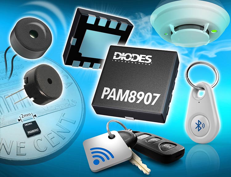
Diodes Incorporated introduces the PAM8907 piezoelectric sounder driver, for maximizing sound pressure level (SPL) delivery from a ceramic/piezo sounder. The PAM8907 has a built-in synchronous boost converter, which extends SPL in battery-powered systems and outperforms other similar sounder drivers. The device is optimized for use in wireless trackers, industrial alarm systems, medical equipment, and domestic appliances.
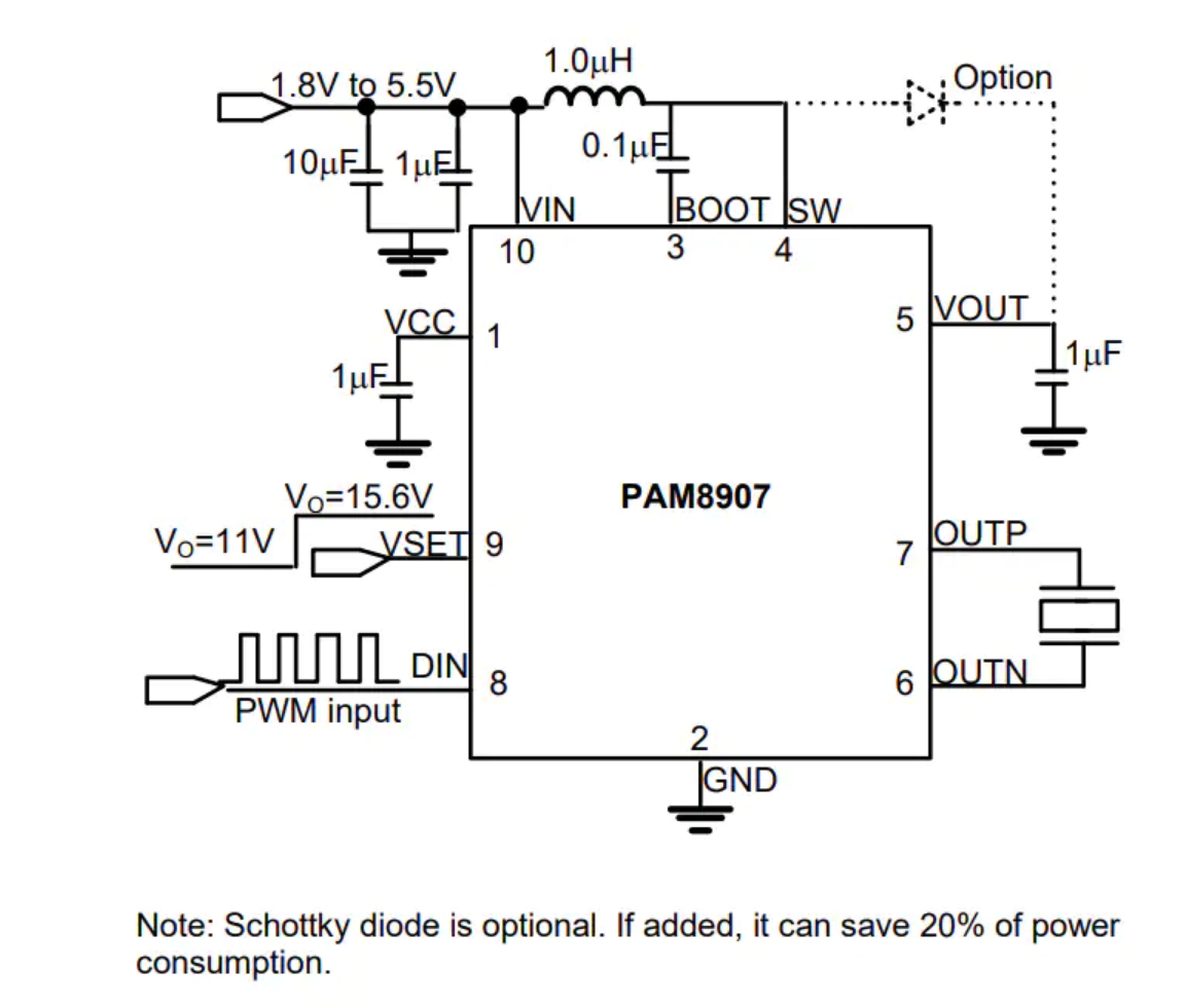
The wide 1.8 V to 5.5 V input voltage range supported by the PAM8907 sounder driver enables it to address a broad variety of potential applications. A 22 VPP or 31 VPP output value can be selected (using the GPIO), thereby providing two different SPL options which allow optimized performance for SPL or battery runtime. Its integrated boost converter requires only a 1.0 µH external inductor which helps reduce the bill-of-materials costs and board space.
Features
Supply Voltage Range from 1.8V to 5.5V
Intergraded Boost Converter VOUT = 11V or 15.6V
Drive Piezo Sounder with up to 31VPP
High-Speed Driver Designed with Very Short Turn-On/Turn-Off
No Voltage Cross Output at Shutdown Mode
High Impendence Output at Shutdown Mode
Low Current Consumption, with Shutdown Current < 1μA
Automatic Shutdown and Wake-Up Control
Available in Space-Saving U-QFN2020-10 package
Totally Lead-Free & Fully RoHS Compliant
Halogen and Antimony Free. “Green” Device
Automatic shutdown and wake-up functions help to further extend the PAM8907 sounder driver’s runtime when incorporated into battery-powered systems, with less than 1 μA of current drawn in shutdown mode. Thermal shutdown, overcurrent, and overvoltage protection, plus undervoltage lockout mechanisms, are included to ensure reliable operation. The product operates across a –40 °C to +125 °C ambient temperature range.
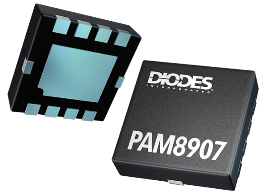
The PAM8907 piezoelectric sounder driver is supplied in the compact 10-pin U-QFN2020 package delivering a minimal footprint. It has a unit cost of $0.43 in 3000 piece quantities.
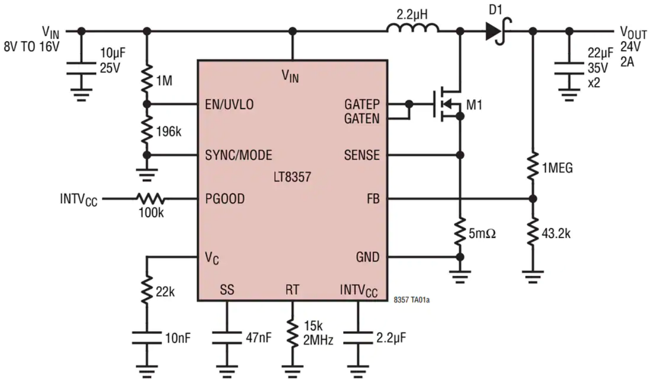
Analog Devices LT8357 Boost, SEPIC & Flyback Controllers are a wide input range, current mode, DC/DC controller which can be configured as a boost, SEPIC, or flyback converter. The LT8357 drives a low-side N-channel power MOSFET with a 5V split gate drive. The current mode architecture allows adjustable and synchronizable 100kHz to 2MHz fixed-frequency operation, or internal 19% triangle spread-spectrum operation for low EMI. At light load, either pulse-skipping mode or low-ripple Burst Mode operation can be selected. Additional features include output power good and output short circuit protection in SEPIC and flyback configurations.
With a wide 3V to 60V input voltage range and 8μA low quiescent current, the Analog Devices LT8357 provides a simple, compact, and efficient solution for automotive, industrial, and battery-powered systems.
Features
3V to 60V wide input voltage range
8μA low IQ Burst Mode® operation
Up to 95% efficiency at 2MHz
±1.5% internal 1V voltage reference
5V split gate drive for efficiency and EMI optimization
Spread-spectrum frequency modulation for low EMI
100kHz to 2MHz fixed switching frequency with external clock synchronization
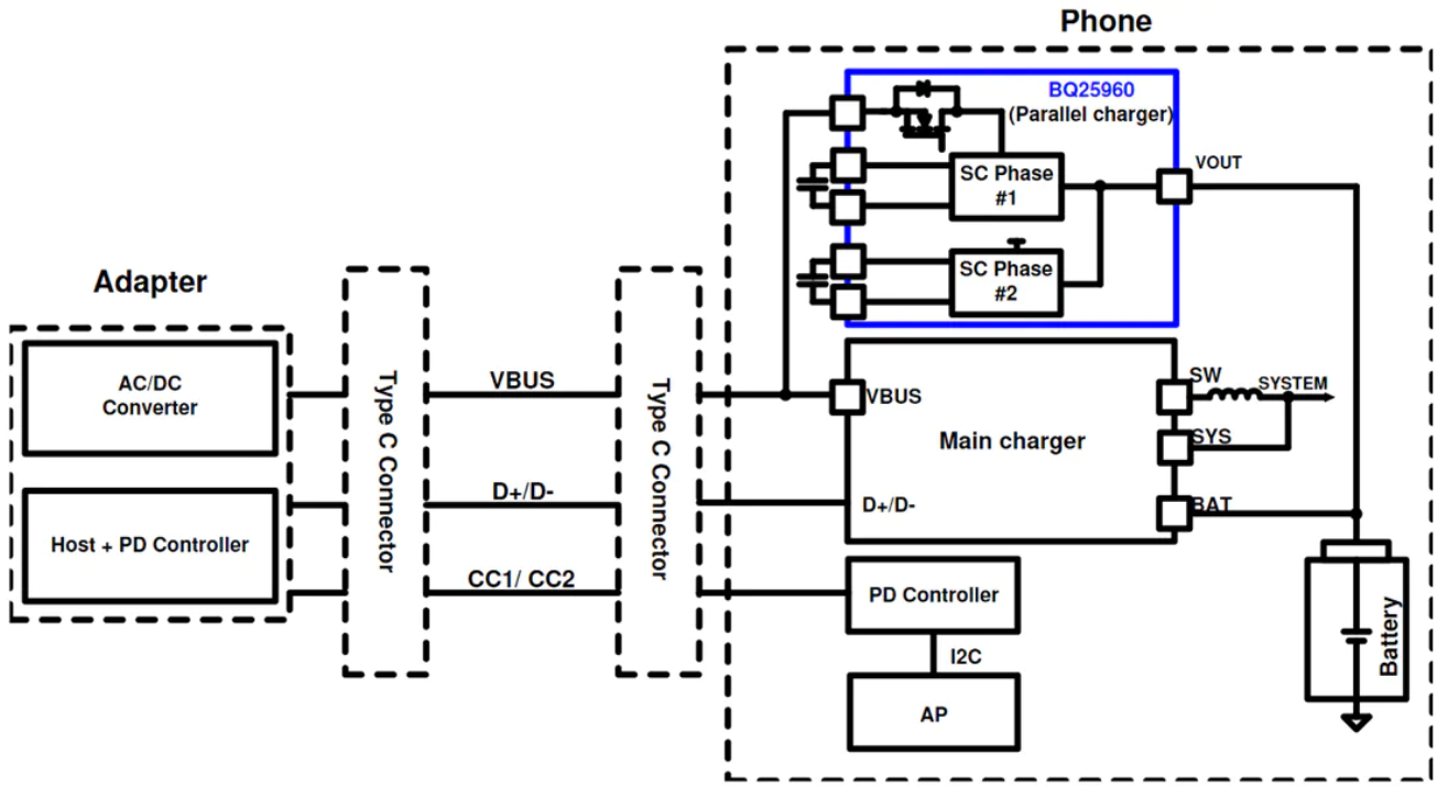
Texas Instruments bq25960 Parallel Battery Charger is a 98.1% peak efficiency, 8A battery charging solution using switch capacitor architecture for a 1-cell Li-ion battery. The switched cap architecture allows the cable current to be half the charging current, reducing the cable power loss, and limiting temperature rise. The dual-phase architecture increases charging efficiency and reduces the input and output cap requirements. When used with the main charger, such as bq2561x or bq2589x, the system enables a full charging cycle from trickle charge to termination with low power loss at Constant Current (CC) and Constant Voltage (CV) Mode.
The Texas Instruments bq25960 supports the 5A Bypass Mode charge (previously called battery switch charge) through internal MOSFETs. The Rdson in Bypass Mode charging path is 21mΩ for high-current operation. The integrated Bypass Mode allows backward compatibility of a 5V fast charging adapter to charge a 1-cell battery. The device supports dual input configuration through integrated mux control and driver for external N-FETs. It also allows single input with no external N-FET or a single N-FET.
The device integrates all the necessary protection features to support safe charging, including input overvoltage and overcurrent protection, output overvoltage and overcurrent protection, input undercurrent and reverse-current protection, temperature sensing for the battery and cable, and junction overtemperature protection in both Switched Cap and Bypass Mode.
The bq25960 includes a 16-bit analog-to-digital converter (ADC) to provide VAC voltage, bus voltage, bus current, output voltage, battery voltage, battery current, input connector temperature, battery temperature, junction temperature, and other calculated measurements needed to manage the charging of the battery from the adapter, or wireless input, or power bank.
Features
98.1% peak efficiency switched-cap parallel charger supporting 8A fast charge
Patent pending dual-phase switched cap architecture optimized for highest efficiency
Input voltage is 2x battery voltage
Output current is 2x of input current
Reduces power loss across input cable
Integrated 5A Bypass Mode fast charge
21mΩ Rdson charging path resistance to support 5A input and 5A output charging current
Dual-input power mux controller for source selection during fast charging and USB On-The-Go (OTG)/ reverse TX Mode
Support wide range of input voltage
Up to 12.75V operational input voltage
Maximum 40V input voltage with optional external ACFET and 20V without external ACFET
Parallel charging with synchronized dual BQ25960 operations for up to 13A charging current
Integrated programmable protection features for safe operation
Input overvoltage protection (BUSOVP) and battery overvoltage protection (BATOVP)
Input overcurrent protection (BUSOCP) and battery overcurrent protection (BATOCP)
Output overvoltage protection (VOUTOVP)
Input undercurrent protection (BUSUCP) and input reverse-current protection (BUSRCP) to detect adapter unplug and prevent boost-back
Battery and connector temperature monitoring (TSBAT_FLT and TSBUS_FLT)
Junction overtemperature protection (TDIE_FLT)
Programmable settings for system optimization
Interrupts and interrupt masks
ADC readings and configuration
Alarm functions for host control
Integrated 16-bit ADC for voltage, current, and temperature monitoring
Suitable for military and industrial systems, the new SA65 Chip Scale Atomic Clock (CSAC) from Microchip enables designers to meet wide operating temperatures, fast warm-up, and improved frequency stability requirements in extreme environments. Featuring ultra-high precision and low power consumption, this new device is form-, fit- and function-compatible with the SA.45s, and helps in improving performance and environmental insensitivity.
The SA65 CSAC is an embedded timing solution with improved environmental ruggedness, has an operating temperature range of -40 to 80 degrees Celsius, and a storage temperature range of -55 to 105 oC. The warm-up time of two minutes at -40 oC is 33% faster than that of the SA.45s. It is the low-power commercial atomic clock that provides precise timing for portable and battery-powered applications requiring continuous operation and holdover in GNSS-denied environments.
This is a highly-portable solution for military applications such as Assured Position, Navigation and Timing (A-PNT) and command, control, communications, computers, cyber, intelligence, surveillance, and reconnaissance (C5ISR) requiring precise frequencies generated by a low Size, Weight, and Power (SWaP) atomic clock.
Key Features of SA65 Chip Scale Atomic Clock
-40°C to +80°C Operating Temperature
-55°C to +105°C Storage Temperature
120 seconds Rapid Warm Up/Atomic Lock
3E-10 Tempco (-40°C to +80°C)
120mW power consumption
17cm3 volume
35g weight
±5.0E-11 accuracy at shipment
1.5 E-11 @1000s Short Term Stability (Allan Deviation)
9E-10 /mo Aging Rate (Typical)
10MHz square wave and 1PPS, both in a CMOS 0V to 3.3V format.
1 PPS input for synchronization
RS-232 interface for monitoring and control
The CSAC family of atomic clocks is supported by Developer Kit 990-00123-000, as well as associated software, a user guide, and technical support. The Chip Scale Atomic Clock products are available for purchase on the company website.
ESP32-C3 is a single-core Wi-Fi and Bluetooth® 5 Low Energy (BLE5) MCU, based on the open-source RISC-V architecture
ESP32-C3 is a single-core Wi-Fi and Bluetooth® 5 Low Energy (BLE5) MCU, based on the open-source RISC-V architecture. It strikes the right balance of power, I/O capabilities, and security, thus offering the optimal cost-effective solution for connected devices.
The availability of Wi-Fi and Bluetooth 5 (LE) connectivity not only makes the device’s configuration easy but also facilitates a variety of use-cases based on dual connectivity.
Key features
State-of-the-art power and RF performance
Unparalleled security for your connected devices
Cost-effective
Wi-Fi and Bluetooth 5 (LE) connectivity
Additional features
CPU and memory:
32-bit RISC-V single-core processor, up to 160 MHz
384 KB ROM
400 KB SRAM (16 KB for cache)
8 KB SRAM in RTC
Interfaces:
22 programmable GPIOs, SPI, UART, I2C, I2S, LED PWM, TWAI, full-speed USB Serial/JTAG controller
Wi-Fi:
IEEE 802.11 b/g/n-compliant
Supports 20 MHz, 40 MHz bandwidth in 2.4 GHz band
1T1R mode with data rate up to 150 Mbps
Bluetooth:
Bluetooth LE: Bluetooth 5, Bluetooth mesh
Speed: 125 Kbps, 500 Kbps, 1 Mbps, 2 Mbps
Advertising extensions
Security:
RSA-3072-based secure boot
AES-128-XTS-based flash encryption
Digital signature peripheral and the HMAC peripheral
Hardware acceleration support for cryptographic algorithms
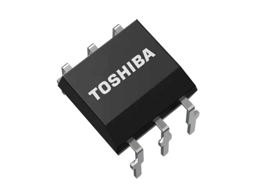
Supplied in a compact DIP6 package, the TLP4590A provides engineers with a more convenient and reliable alternative to conventional mechanical relays
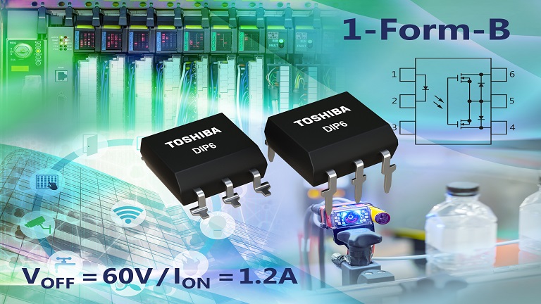
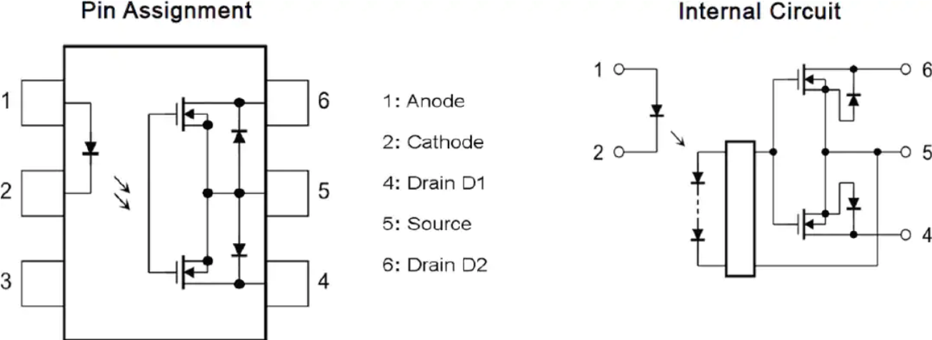
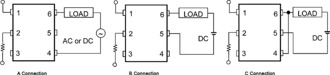
Supplied in a compact DIP6 package, the TLP4590A provides engineers with a more convenient and reliable alternative to conventional mechanical relays. This 1-Form-B (normally closed) photorelay with a MOSFET output, has an ON-state current rating of 1.2 A, which represents a 140% improvement on the previous-generation TLP4176A device. In addition, it has a 60 V OFF-state output terminal voltage rating. Its sensitivity is enhanced thanks to the low trigger LED current of 2 mA (maximum) exhibited.
Key features
1-Form-B (normally closed)
VOFF = 60 V/ION = 1.2 A
Low trigger current 2 mA
High isolation voltage BVs = 5000 VRMS
Additional features
Direct replacement of mechanical relays together with 1-Form-A (normally open) device
Long lifetime and high reliability compared with mechanical relays
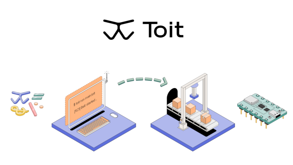
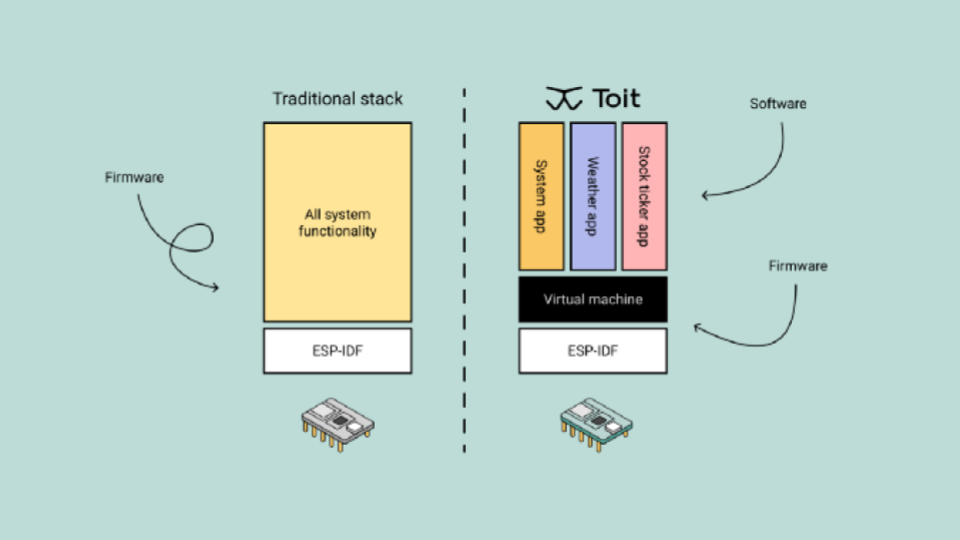
Toit revolutionizes the IoT development process by offering a novel approach that fixes most of the issues inherent to the traditional process. Toit provides you with everything needed for developing an IoT application: firmware, cloud connectivity, a web-based console, and even a new programming language with syntax similar to Python but much faster execution speeds. This article presents some notable features of this all-in-one platform which help IoT developers to build their applications quickly and easily.
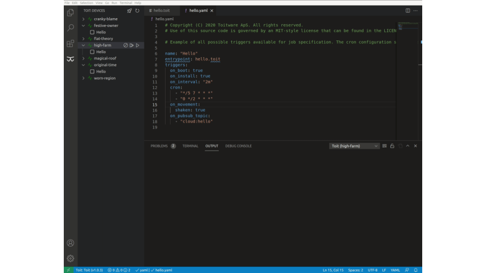
Deploy your First Application from Scratch within 15 Minutes
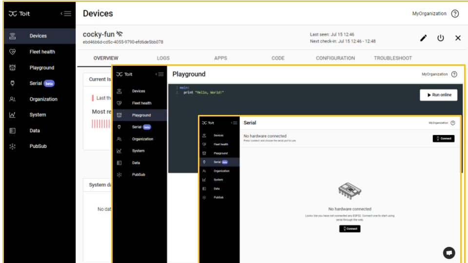
Toit provides a smooth onboarding process for developers who are new to this platform. First-time users need an ESP32 board and a USB cable to flash the firmware. This is a one-time process and future updates for the firmware will be done over the air. After signing up, the web-based console provides almost everything for getting started. Now with the support for flashing from the browser using Web serial, users can start developing even without installing anything on their PCs. This whole process of provisioning your device will take a few minutes and you’ll be up and running.
The console provides an inbuilt code editor where you can write, run code on your device and monitor the output with timestamps. This is a great way to quickly try out something and improve your program. Finally, when your program is working as expected, you can deploy it as a long-lived application on your device. If any, the output of the app will be logged and can be seen through the console under the LOGS section.
Efficient Multitasking on a $2 MCU
The multitasking capability of Toit is what makes it stand out from the crowd. On top of that, the isolated memory areas for each application put the icing on the cake. This way, the security of data is taken care of. Multitasking on an MCU with the traditional development process is not impossible but might easily break the whole system even if a small bug comes up. On Toit, it is a light and agile process, so users can easily try out new things without having to worry about bricking the device.
In fact, multiple applications run independently on the device. So, even if one of the apps goes down, the others won’t be affected and the system will keep running normally. Users can just fix the buggy app and re-deploy it as before.
Easy to Use Programming Language and APIs
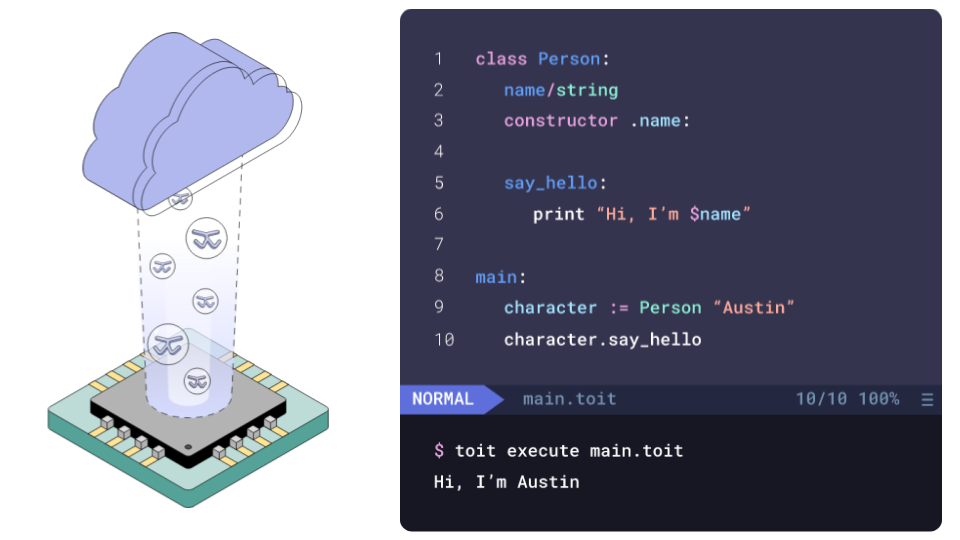
Traditional IoT programming can be done using a lot of programming languages, with C/C++ and MicroPython being the popular ones. The problem here is that writing with low-level language might be painstaking when it comes to microcontrollers. On the other hand, high-level languages like MicroPython make it easy to write code but you’ll have to sacrifice the execution speeds. Toit decided to change everything by creating a new dedicated programming language for IoT. The Toit programming language has syntax similar to Python but is 20 times faster than MicroPython. This new language comes with an automatic memory management system which helps to avoid crashes.
Toit also provides a publicly available gRPC API allowing users to have complete control over their devices through a client application. As Toit engineers put it, “You are in full control of your devices and everything you can do with the Toit platform, you can do through our API. It is easy to integrate our platform into your products and turn your device fleet fully programmable.” The API definitions and examples are available on their Github repo.
Visual Studio Code Extension to Write and Deploy Apps
Syntax highlighting has become a necessity nowadays for writing any type of code. With the introduction of a new programming language, Toit released a VS code extension that does much more than just highlighting the code. Users can run code snippets, deploy apps and monitor the output in the inbuilt terminal. The extension also gives an overview of devices and apps running in the sidebar. So altogether, this VS code extension covers all the basic functionalities of the web-based console, while providing a few additional tools for app deployment.
Support for Raspberry Pi is available as a Beta Program
Apart from ESP32, Toit has now released a beta program for working on Raspberry Pi devices as well. Traditionally, Raspberry Pi IoT devices may require as much as 200 MB of code updates. With Toit, the updates are around 50 KB which takes less than 2 seconds to be installed. These updates are small enough to be sent across low-bandwidth cellular connections like NB-IoT or Cat-M1. Developers can also swap their Raspberry Pi with an ESP32 while keeping the same code stack. This way, Toit comes up as a hardware-independent IoT platform.
You can learn more about the Toit IoT platform and its features on their website.
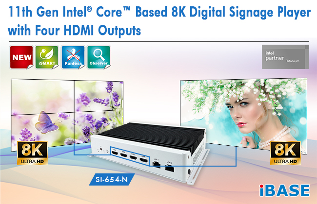
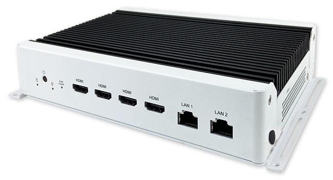
IBASE Technology Inc., a leading provider industrial computing and innovative digital signage solutions, launches its SI-654-N fanless digital signage player powered by Intel’s latest 11th Gen Core™ U-Series processors (formerly Tiger Lake) manufactured with Intel’s 10nm SuperFin transistor that achieves up to 17.5% performance uplift and significantly higher clock speeds at lower power compared to the original 10nm.
The SI-654-N is currently offered with an Intel® Core™ i7-8665UE processor (8M Cache, up to 4.40 GHz) integrating the high-performance Iris Xe GPU, Intel’s 12-Gen graphics with 96EUs. Measuring 200 x 139 x 41 mm, the compact SI-654-N can be easily installed in space-constraint environments. It houses four HDMI 2.0 connections to deliver up to 1x 8K display or 4x 4K displays, performing a vivid 8K resolution and ensuring a truly immersive audience’s viewing experience.
Mainly designed for digital signage in busy places where there is a constant demand for practical information, the SI-654-N features HDMI-CEC control, display status monitoring, flexible video wall configurations and hardware EDID emulation that prevents distorted or black screen due to display and cable connection issue.
“The new industrial-grade SI-654-N is perfectly suited for video wall solutions in airports, shopping malls and other commercial premises that require reliable 24/7 operation,”
said Archer Chien, director of solution product planning at IBASE.
“With our advanced iSMART and Observer technologies, the SI-654-N is equipped with low temperature boot protection, power resume control, power on/off scheduling, and hardware monitoring to enable continuous and stable operation.”
SI-654-N FEATURES:
iSMART intelligent energy-saving technology – enables power on/off scheduling and power resume functions
11th Gen Intel® Core™ U-series processor (Tiger Lake platform)
1x M.2 E-key (2230) for WiFi or capture card option
TPM 2.0, vPro and watchdog timer
Industrial-grade robust, fanless and compact design
For the deployment of high computing performance signage, the model SI-654 with cooling fan is also available. Both players support TPM 2.0 for optimal cyber security and vPro for easy remote monitoring and management. A webinar to introduce the player will be hosted on August 31th via Digital Signage Today.
Register now to learn more details with the SI-654-N!
Author: Marian Hryntsiv, Documentation Engineer, Dialog Semiconductor
Introduction
There is a variety of applications where a mechanical potentiometer is part of a user control interface. These mechanical potentiometers can be changed to more updated and reliable encoder-controlled elements and digital rheostats, being components that change the electrical parameters of the signal.
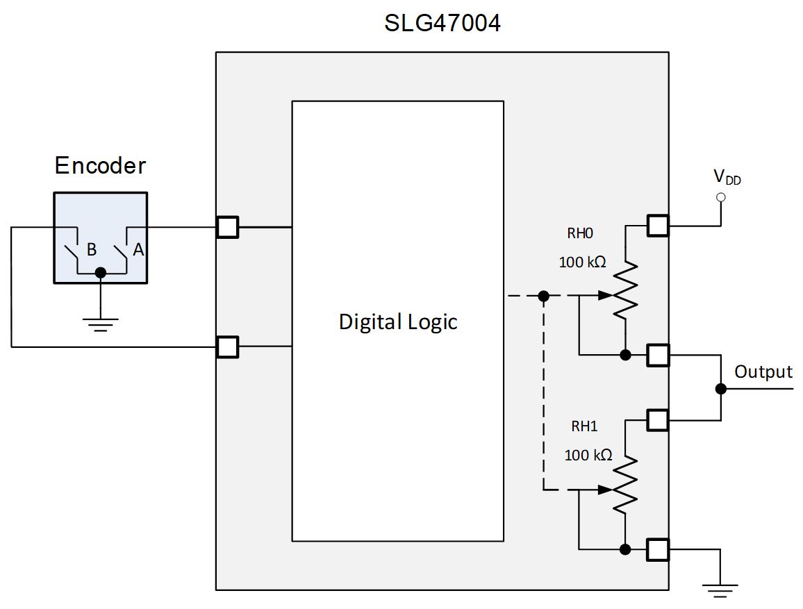
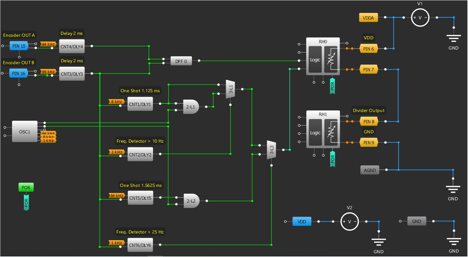
In this article, we used GreenPAK™ SLG47004. It is a great choice for this project as this circuit combines two digital rheostats and configurable logic to process the encoder information. This combination allows the implementation of many designs: a regulated power supply, an amplifier with a tunable gain, and others. In addition, the presence of digital logic allows determining the speed of rotation of the encoder. This approach is shown in Figure 1.
Figure 1: General Schematic of a Voltage Divider Controlled by the Encoder
1. System Overview
Figure 2 shows the internal circuit design based on the SLG47004.
Figure 2: GreenPAK Designer Project
The complete design file created in free GUI-based software – GreenPAK Designer – can be found here.
An incremental encoder generates its A and B output signals which are used to change digital rheostats resistance. Rheostats form the potentiometer and allow the implementation of the adjustable voltage divider to regulate an output voltage.
At any time, the phase difference between the A and B signals will be positive or negative depending on the encoder’s direction of movement.
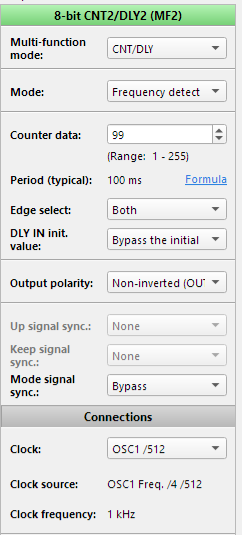
A speed determination function is built from Frequency Detectors, One-Shots, and Multiplexers.
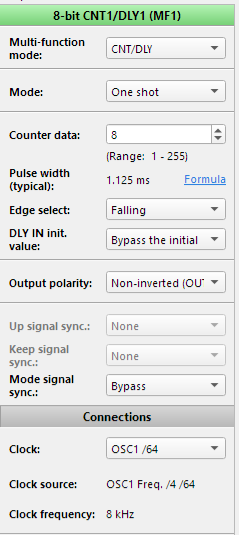
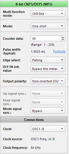
In this article, the EC11 encoder was used. The encoder produces noisy output oscillations due to a switch bounce. To eliminate that noise, 2 mS delays were used. Please note that this delay is adjusted for the EC11 encoder (according to its datasheet). For other encoders, the delay value should be assessed accordingly.
2. Functional Block Architecture
2.2. Digital Logic Description
2.1.1. Determining the Encoder Direction
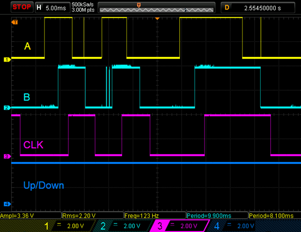
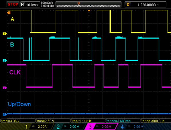
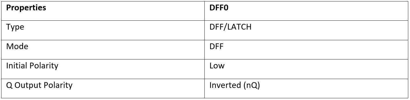
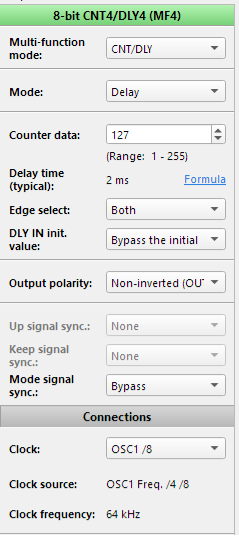
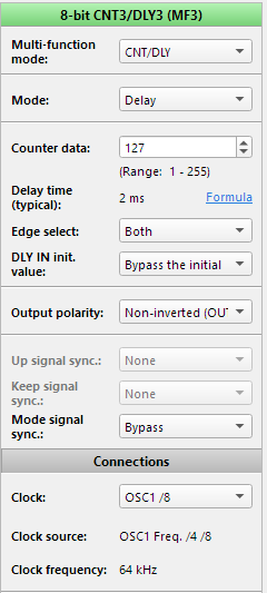
At first, Delay macrocells delay both edges of the encoder output signals for 2 mS. Delay macrocells work like a deglitch filter to eliminate switch bouncing. Delayed signal B appears on DLY inputs of One-Shots and Frequency Detectors, and CLK input of DFF. Delayed signal A appears on the D input of DFF. When the encoder disk is rotating in a clockwise direction signal A leads signal B and DFF output is High, and when the disk is rotating in a counterclockwise direction signal B leads signal A and DFF output is Low. So DFF can determine the direction of rotation. High or Low signal on Rheostat Up/Down input determines if internal counter’s value increases or decreases for each pulse at CLK input.
A timing diagram for the clockwise encoder rotation is shown in Figure 3 and for the counterclockwise encoder rotation in Figure 4.
Figure 3 Timing Diagrams for Clockwise Encoder RotationFigure 4 Timing Diagrams for Counterclockwise Encoder Rotation
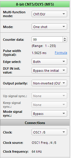
2.1.1. Determing the Encoder Speed
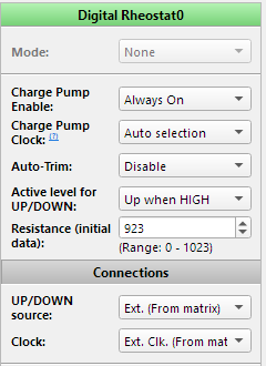
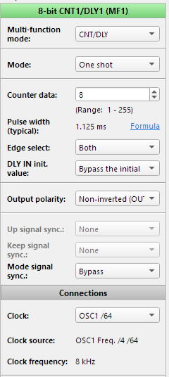
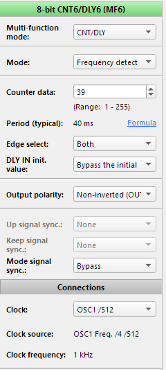
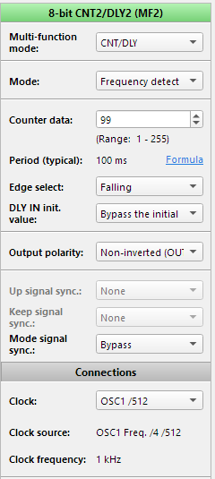
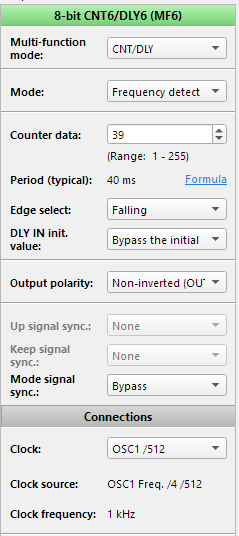
The SLG47004 has 10-bit digital rheostats, which in turn allows the implementation of 1024 regulation steps. The adjustable voltage divider has 3 regulation modes. The user can change output signal with step = 1 digital code (mode 1), step = 10 digital codes (mode 2) and step = 100 digital codes (mode 3). 2 frequency detectors were used to have 3 modes. The first mode is assigned to adjust the output signal smoothly and accurately. It activates when a user adjusts a knob with a frequency less than 10 Hz. The second mode activates when the frequency is greater than 10 Hz, but less than 25 Hz. The last one works when the frequency is greater than 25 Hz.
One-Shots set time intervals for the required number of pulses.
Digital multiplexers provide the passage of either one, or ten, or hundred pulses on CLK input of rheostat according to frequency detectors outputs.
2.1.2. Detents and Pulses per Revolution
The encoder with a different number of pulses and detents (positions) was used in this project. With 15 pulses, you have two detents per full pulse. This means that for every pulse (or cycle) in the rotary encoder there are two detents: rising edge of the pulse (one change) and falling edge of the pulse (another change). If your rotary encoder has one detent per pulse, then it has two changes for every pulse. For this type of encoder, the design remains the same, except for Frequency Detectors and One-Shots settings. In their settings, Edge Select should be set “Falling” or “Rising”. In encoders where the number of pulses and detents do not match, Edge Select should be set to “Both”.
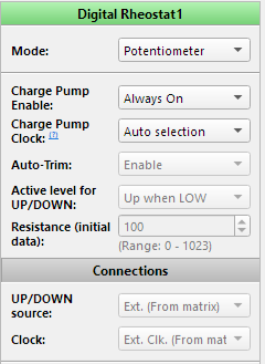
2.2. Potentiometer Mode
For this design, we used digital rheostats in potentiometer mode. This mode allows two 2-pin rheostats to work as one 3-pin potentiometer. When this mode is active (register [917] = 1), the user changes the value of the RH0 internal counter. In this mode, the value of the RH1 counter is the inverted value of the RH0 counter. Note that the RH0_B pin and the RH1_A pin must be connected externally.
2.3. Macrocells Settings
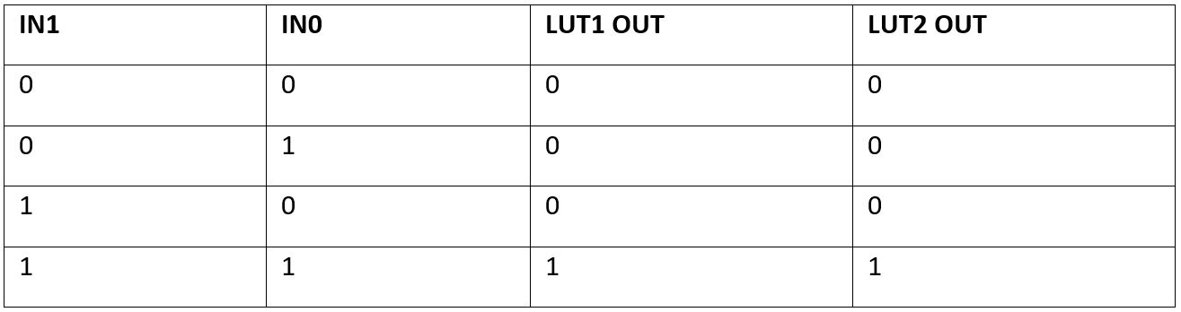
The following tables present 3-bit LUT1 and 3-bit LUT3 settings: Standard Gate – Multiplexer.
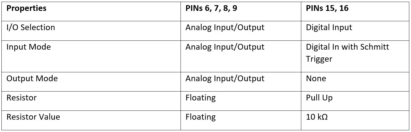
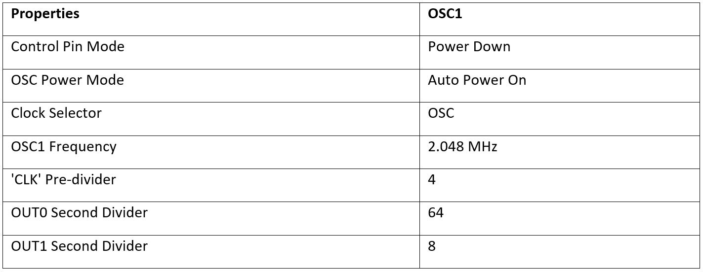
Table 1: 2-bit LUTs SettingsTable 2: DFF SettingsTable 3: PINs SettingsTable 4 OSC SettingsFigure 5a Digital Rheostats SettingsFigure 5b Digital Rheostats SettingsFigure 6a Delays SettingsFigure 6b Delays SettingsFigure 7a One Shots Settings when the Number of Pulses and Detents Do Not MatchFigure 7b One Shots Settings when the Number of Pulses and Detents Do Not MatchFigure 8a One Shots Settings when the Number of Pulses and Detents MatchFigure 8b One Shots Settings when the Number of Pulses and Detents MatchFigure 9a Frequency Detectors Settings when the Number of Pulses and Detents Do Not MatchFigure 9b Frequency Detectors Settings when the Number of Pulses and Detents Do Not MatchFigure 10a Frequency Detectors Settings when the Number of Pulses and Detents MatchFigure 10b Frequency Detectors Settings when the Number of Pulses and Detents Match
Conclusions
The SLG47004 has two digital rheostats which allow implementing a myriad of useful applications. A case in point is using digital rheostats to replace an analog potentiometer with the help of a modern encoder. This article illustrates how to use the SLG47004 to implement the adjustable voltage divider which is a versatile solution and can be applied to an adjustable power supply, amplifier’s gain control, and others. This solution is cost-effective and has low energy consumption.
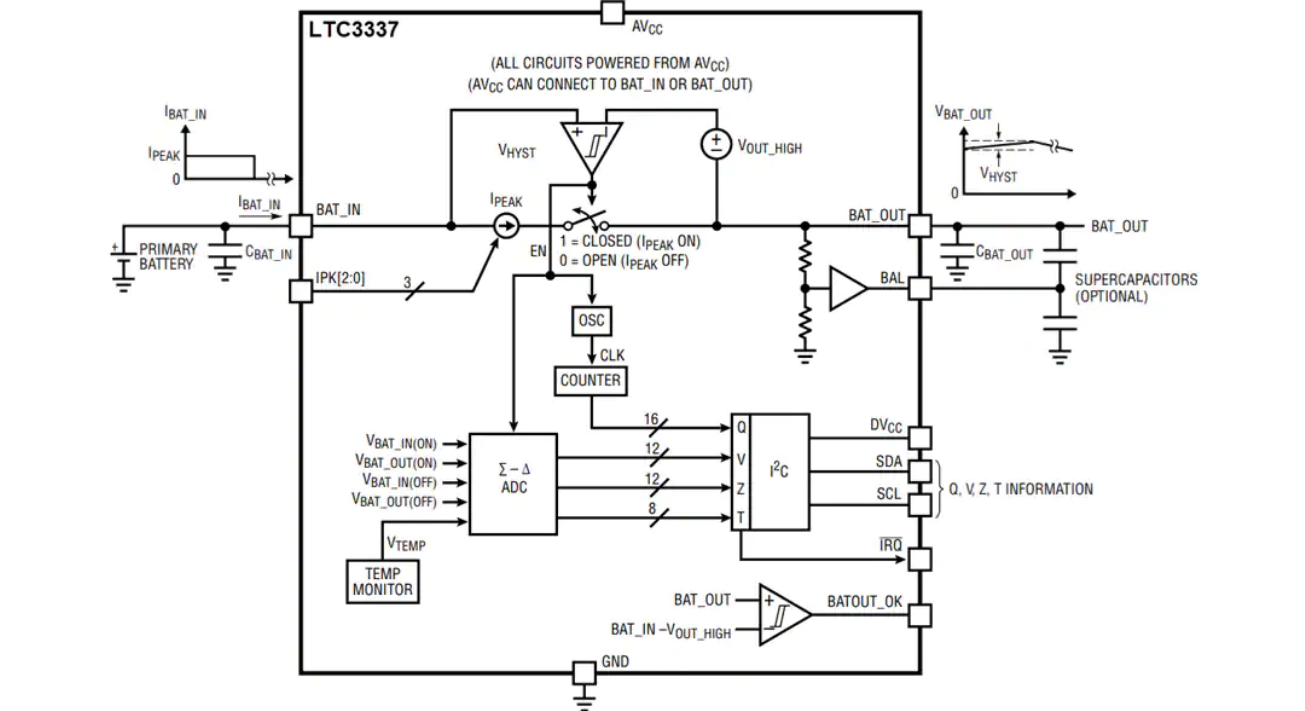
Analog Devices Inc. LTC3337 Primary Battery State of Health (SOH) Monitor provides accurate, real-time readings of battery cell discharge, voltage, impedance, and temperature. The LTC3337 is designed to be placed in series with a primary battery with minimal associated series voltage drop. This device integrates an infinite dynamic range coulomb counter that tallies all accumulated battery discharge and stores it in an internal register accessible via an I2C interface. A discharge alarm threshold based on this state of charge (SOC) is programmable. When it is reached, an interrupt is generated at the IRQ pin. Coulomb counter accuracy is constant down to no load.
To accommodate a wide range of primary battery inputs, the peak input current limit of the LTC3337 is pin selectable from 5mA to 100mA.
Coulombs can be calculated for either the BAT_IN or BAT_OUT pin, determined by the AVCC pin connection. A BAL pin is provided for applications utilizing a stack of two supercapacitors (optional) at the output.
The Analog Devices Inc. LTC3337 Primary Battery State of Health Monitor is available in a 12-lead Lead Frame Chip Scale Package (LFCSP) with an exposed pad for improved thermal performance.
Internal Diagram
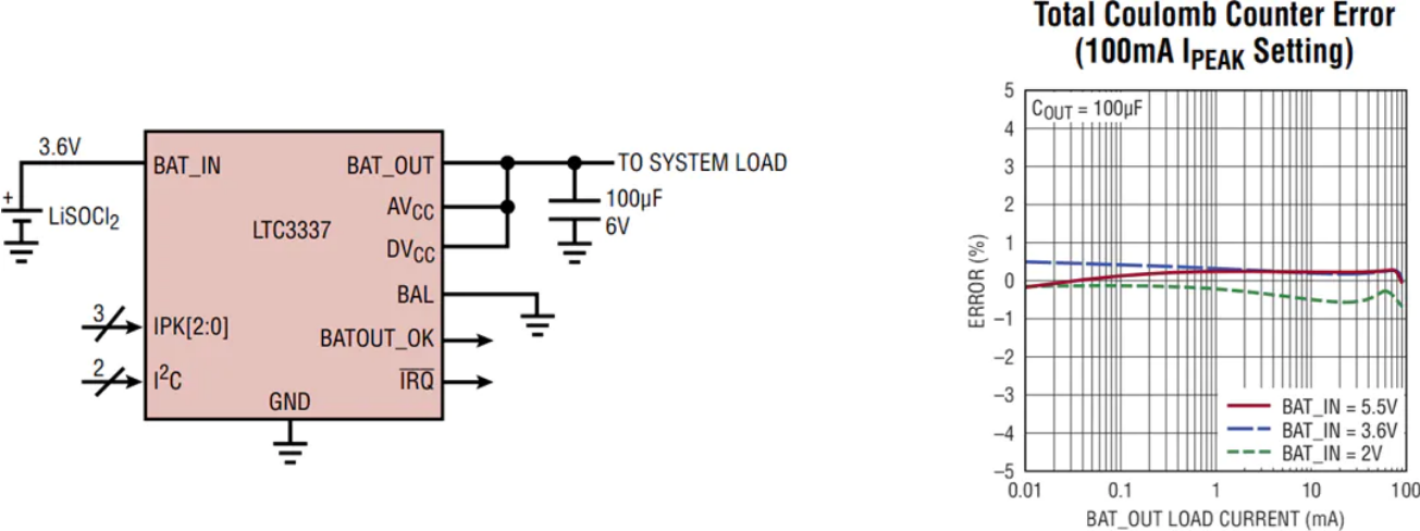
Application Diagram
Features
8.0V to 5.5V battery input voltage range
100nA quiescent current
8 primary battery peak input current limits
5mA, 10mA, 15mA, 20mA, 25mA, 50mA, 75mA, 100mA
SOH monitor for primary battery
Integrated coulomb counter (Q)
Additional monitors for battery voltage (V), battery impedance (Z), and temperature (T)
Integrated ±10mA supercapacitor balancer
Primary battery current (BAT_IN) or load current (BAT_OUT) is counted
Programmable coulomb counter prescaler for a wide range of battery sizes
Programmable discharge alarm threshold with interrupt output
I2C interface
-40°C to +125°C operating junction temperature range