Researchers at the University of Washington (UW) have created A new kind of PCB what they are calling a “Vitrimers PCB” or vPCB for short. The unique characteristic of this PCB is that it’s made to be recycled. In the lab, scientists manufactured functional prototypes of Internet of Things (IoT) devices transmitting 2.4 GHz radio signals on vPCBs then they recycled that PCB and recovered 98% of the vitrimer and 100% of the glass fiber, as well as 91% of the solvent used for recycling.
The UW team also tested the Vitrimer PCB for its electrical, thermal, and mechanical properties and found that they are very similar to standard FR-4 PCB material. This suggests that Vitrimer PCBs could offer a viable solution to reduce landfill waste by facilitating the recycling of leftover copper, thereby maximizing resource recovery.
Vitrimers are a new class of plastics that are both strong and reprocessable. Unlike traditional thermosets, which are permanently hardened after being formed, vitrimers can be reshaped and recycled multiple times without losing their properties. This is because vitrimers have dynamic chemical bonds that can be broken and reformed with the application of heat, enabling them to be molded like glass. This unique ability makes vitrimers promising for a variety of applications where durability and sustainability are important.
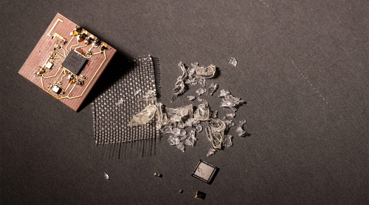
A solvent is dissolving the VPCB
A solvent dissolves the vitrimer in vPCBs, separating it into a jelly-like substance for easy recovery of glass fibers and metal traces. Researchers were able to recover 98% of the vitrimer, 100% of the glass fiber, and 91% of the solvent. This recycling process could reduce the global warming potential by 48% and carcinogenic emissions by 81% compared to traditional PCBs.
While the new Vitrimers PCB appears to be a promising green solution, its real-world adoption depends on a few factors: it needs to be affordable to produce, there should be incentives in place to encourage the recycling of electronic waste, and more research is needed to ensure it can perform well in high-speed and demanding applications.
vPCB got dissolved into the solvent and only the fiberglass part is remaining
Key Features of Vitrimers-based Recyclable PCB:
Utilizes vitrimer epoxy, a polymer capable of repeated curing and uncuring without deterioration.
Environmentally conscious design aimed at reducing electronic waste and promoting a circular lifecycle for electronics.
Maintains electrical and mechanical performance similar to commonly used FR-4 PCB materials.
Recyclability features include repairability under heat and pressure, easy removal of components for reuse or responsible recycling, and the ability to recover and reuse base vitrimer and glass fibers in new PCBs.
Demonstrates high recovery rates for vitrimer, glass fiber, and solvent used in the manufacturing process.
Compatible with existing PCB manufacturing processes, requiring minimal adjustments.
More information on this Vermiters-based recyclable PCB can be found on the UW news page. The researchers mention that further research is ongoing to develop even better vitrimer materials for a wider range of applications.
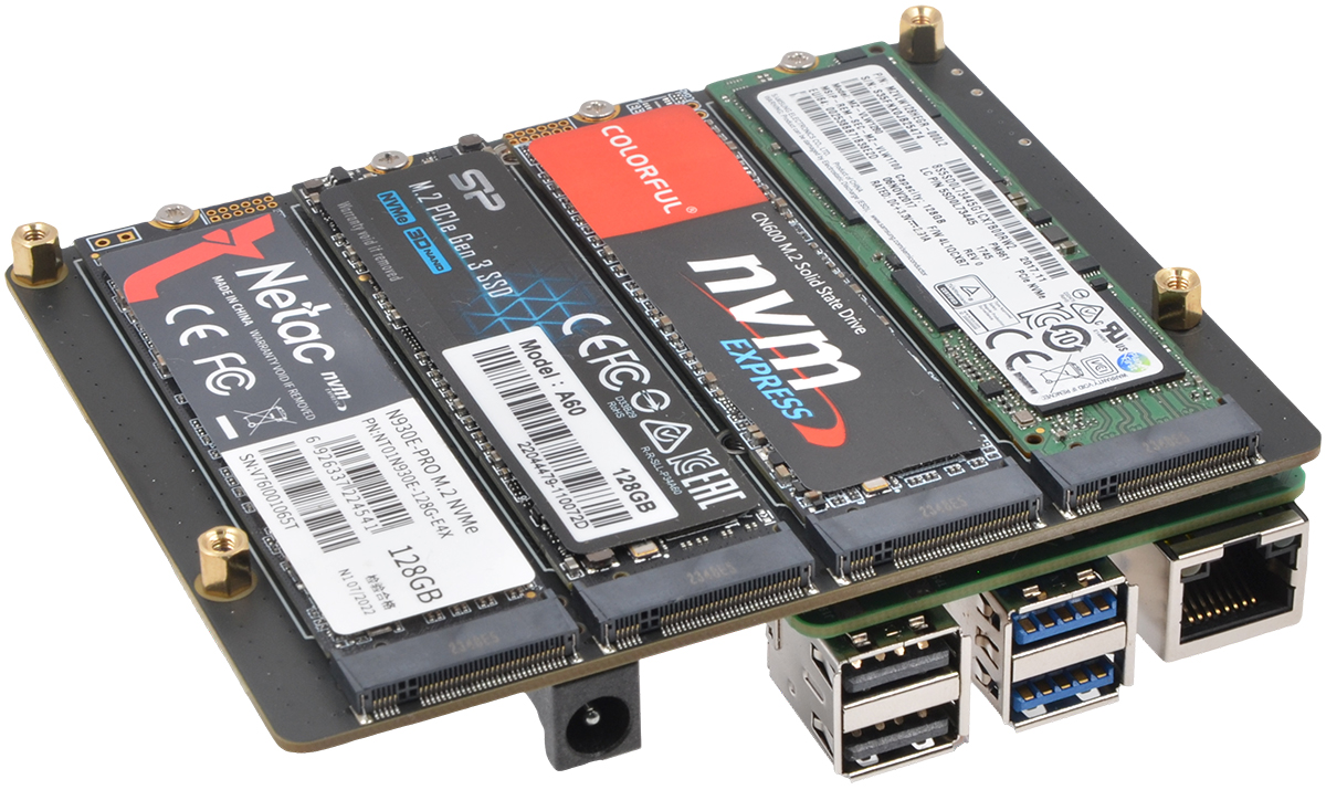
SupTronics X1011 is a HAT for Raspberry Pi5 that uses the latest HAT+ standard to add in up to four M.2 NVMe SSDs to the Pi making it a great option for building a DIY! NAS. The HAT connects to the Pi and other SBCs with the PCIE Interface and offers PCIe Gen2 transfer speeds.
The company mentions that the HAT works with PCIe GEN2 Speeds, though it can be configured to PCIe Gen 3, however, this is not advantageous because the PCIe switch only supports PCIe Gen 2 x1. On top of that, this solution will provide approximately the same sequential read/write performance as SATA hard drives. But the good thing will be that it’s now in a small form factor. Despite this limitation, random I/Os are expected to perform considerably faster, for more technical details and instructions to get started, you can check out their wiki page.
To test the board to its capacity Jeff Geerling conducted performance tests on the sample and compared it to the FriendlyELEC CM3588 NAS Kit powered by the Rockchip RK3588, which is slightly pricier at around $20 more. The CM3588 NAS Kit boasts a PCIe Gen3 x4 interface, offering significantly better performance than the Raspberry Pi 5’s PCIe Gen2 x1.
SupTronics X1011 Specifications
Supported SBC: Compatible with Raspberry Pi 5 and other SBCs featuring a compatible 16-pin PCIe FPC connector and mounting holes
Chipset: ASMedia ASM1184e PCI express packet switch with 1x PCIe Gen2 x1 upstream port and 4x PCIe Gen2 x1 downstream ports
Storage Capacity: 4x M.2 sockets supporting up to 16TB storage capacity (4x 4TB) with M.2 NVMe 2280/2260/2242/2230 SSDs (SATA not supported)
NVMe Boot: Not supported due to the current lack of Raspberry Pi firmware support for PCIe switches
Power Management:
5V/5A DC via FFC & pogo pins (utilizing the USB-C port on the Pi 5)
5V/5A DC via 5.5/2.1mm DC power jack
DC/DC step-down converter delivering a maximum of 10A to power the SSDs
Compatible with HAT+ standby power state, automatically turning off when the Raspberry Pi 5 shuts down
Caution: Do not power the Raspberry Pi 5 through its USB-C port simultaneously if using the DC jack
Dimensions: 109 x 87.2mm
More details about the new SupTronics X1011 SSD board can be found on the SupTronics website. While SupTronics does not sell directly to consumers, Geekworm is the first retailer to offer the board in single units. As a special launch offer, the board is currently available for $51, discounted from its planned retail price of $55.
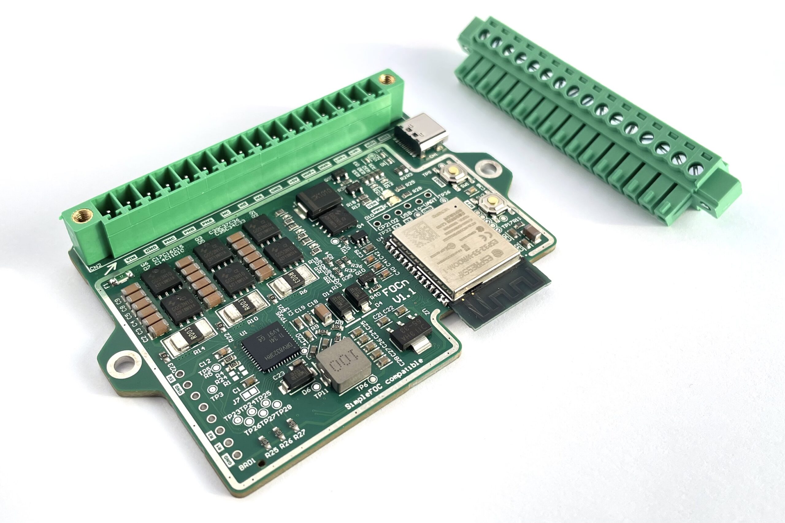
Matej Planinšek of PLab, has developed the FOCn – A ESP32-S3-based medium-power BLDC Motor driver module that has the capability of delivering up to 10A of continuouscurrent. The USP of this device is that it supports SimpleFOC Arduino Library making it easy to control BLDC and stepper motors with the field-oriented control algorithm.
The FOCn module uses the ESP32-S3ESP32-S3 MCU and offers Wi-Fi and Bluetooth connectivity. Additionally, the microcontroller supports ESP-NOW, a proprietary low-power, low-latency communication protocol designed by Espressif Systems. This unique feature enables seamless communication between multiple FOCn boards, fostering synchronized control and coordinated operation.
The developer was inspired to create the FOCn module when their search for a custom-made, SimpleFOC-compatible driver module that met all their requirements failed. The name is related to field-oriented control (FOC) and also means “face slap” in Slovenian, Matej’s native language.
The module has an onboard USB-C port that can be used to program and debug the driver module. The MOSFETS used in the module can drive loads mode that 10A. But Extra cooling (heat sink or cooling fan) is required to dissipate the heart that this load will generate.
The FOCn project is open-source meaning that you can get all the schematics, Altium files, and documentation for the project on their GitHub repo along with platform examples. If you want to get your hands on one you can do that as it is available on Tindie for $64.
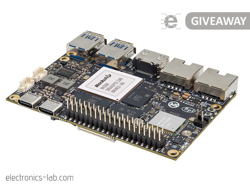
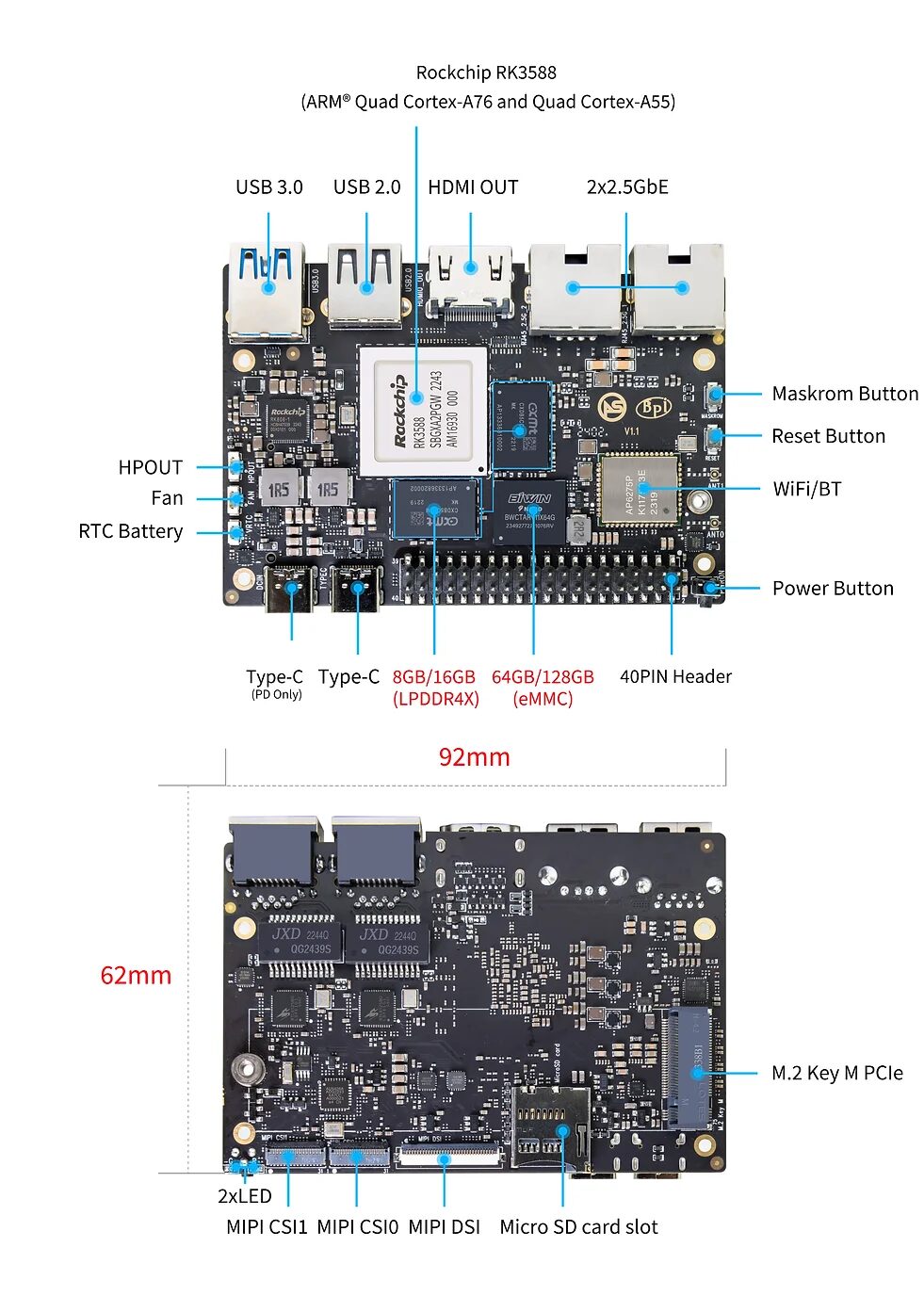
The ArmSoM Sige7 is a compact single-board computer (SBC) powered by an octa-core 64-bit SoC with a 6TOPS NPU for AI tasks and supports up to 32GB of LPDDR4x RAM and 128GB of eMMC flash storage. It includes an M.2 2280 socket for NVMe SSDs. It offers three display interfaces (HDMI, USB-C, MIPI DSI) and two camera connectors. Connectivity options include dual 2.5GbE,WiFi 6, and Bluetooth 5.2, plus multiple USB ports and a 40-pin GPIO header for expansion.
Are these specs exactly what you’ve been looking for? If you’re ready to upgrade, get excited! We’re hosting a giveaway for this amazing product, and we will give away 1 x Sige7 to our readers. Check out the instructions below to enter for your chance to win!
The giveaway ends in:
The giveaway is over! Comments are closed and it’s time to select the winner.
The draw will take place on Monday – 20 May 2024.
The winner is… comment #29 -> Hüseyin Avni Sarıkaya, congrats!
ArmSoM SIGE7 Specifications:
CPU: Quad-Core [email protected]+Quad-CoreCortex-A55@ 1.8GHz,8nm process
6 TOPS@INT8(3 NPU core)
GPU&VPU: GPU Mali-G610 MP4 (4x256KB L2 Cache)
Decode: 8K@60fps
Encode:8K@30fps H.265 / H.264
Storage: 8GB LPDDR4x + 64bit 64GB eMMC 5.1
Interface: 2x 2.5G Ethernet
Onboard IEEE 802.11a/b/g/n/ac/ax WIFI6 and BT5 (AP6275P)
1x HDMI 2.1, supports 8K@60fps
1x DP 1.4 up to 8192×4320@30Hz
1x MIPI DSI up to 4K@60Hz
2x 2-lane MIPI CSI, up to 2.5Gbps per lane
Board Layout
Giveaway Prize: ArmSoM Sige7 (basic model worth $165)
Ready to win? Here’s how to enter our awesome giveaway:
Drop a comment! Tell us your country and anything else you’d like to share (but please, no links!). Missing your country will mean your entry won’t count.
One entry per person, please. We’ll be keeping an eye out for duplicate entries.
The winner will be chosen randomly and announced in the comments section. We’ll contact you by email, so make sure to use a real one – you’ll have 24 hours to respond!
Electromagnetism is a branch of physics and engineering that includes the study of electric and magnetic fields and their interactions. Electricity and magnetism are two aspects of electromagnetism. This concept describes how electric currents create magnetic fields and how changing magnetic fields induce electric currents. Electromagnetism involves phenomena such as electromagnetic induction, electromagnetic waves (including light), and the behavior of charged particles in electric and magnetic fields.
In physics, electromagnetism is one of the fundamental forces of nature. In engineering, electromagnetism plays a crucial role in various disciplines such as electrical engineering, electronics, telecommunications, and electromechanical systems. Engineers always utilize principles of electromagnetism to design and develop devices like motors, generators, transformers, antennas, and communication systems.
Historically, electricity and magnetism were long thought to be separate forces. It was not until the 19th century that they were finally treated as interrelated phenomena. In 1905 Albert Einstein’s special theory of relativity established that both are aspects of one common phenomenon.
An important aspect of electromagnetism is the science of electricity, which is concerned with the behavior of aggregates of charge, including the distribution of charge within matter and the motion of charge from place to place.
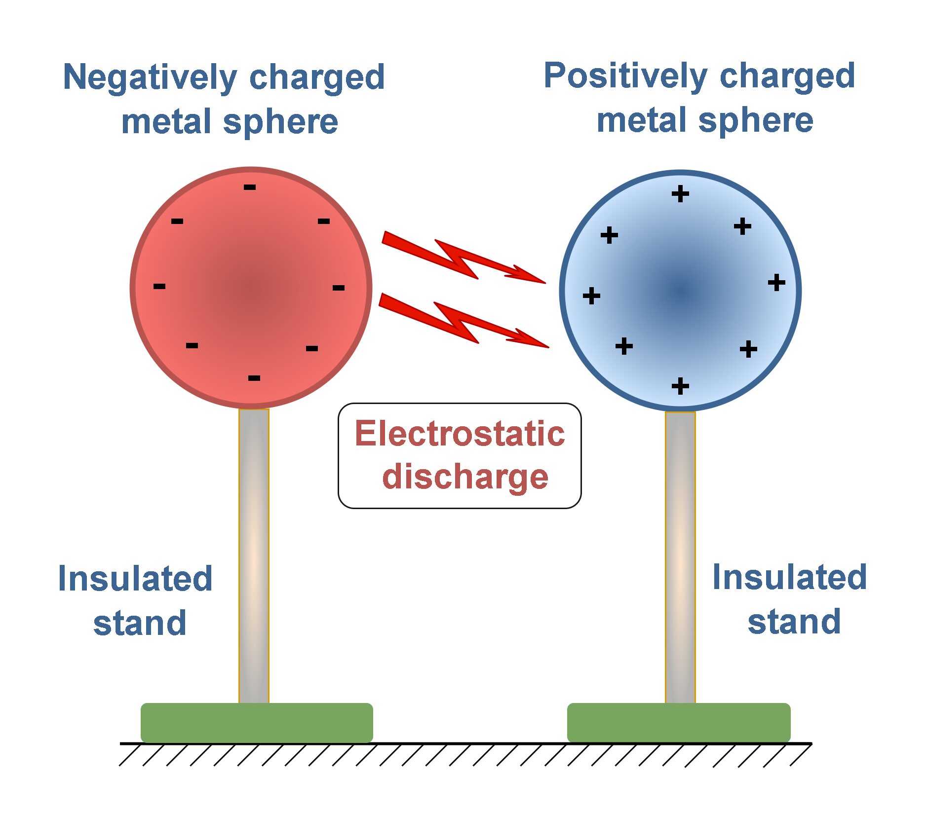
At a microscopic scale, the electric force in particular is responsible for most of the physical and chemical properties of atoms and molecules. It is strongly compared with the force of gravity. At a more familiar macroscopic scale, electric phenomena are responsible for the lightning and thunder accompanying certain storms in nature. Such conditions can be simulated in a laboratory with two oppositely charged metal spheres which are installed on insulated stands. If we bring them close to each other, in a certain distance we may observe some sparks because of electrical discharge between spheres, as Figure 1 shows.
Figure 1: The electrical discharge phenomenon
Electricity is the lifeblood of technological civilization and modern society. Without it, we revert to the mid-nineteenth century: no telephones, no television, none of the household appliances that we take for granted. Instead, with the discovery and harnessing of electric forces and fields, we can view arrangements of atoms, probe the inner workings of the cell, and send spacecraft beyond the limits of the solar system.
Static Electric Charges
Electrostatics is a branch of physics that studies the interaction between slow-moving or stationary electric charges. It focuses on phenomena involving static electricity, where charges are not in motion.
Around 600 B.C. the ancient Greek philosophers conducted the earliest known study of electricity. It all began when Thales noticed that a fossil material called amber would attract small objects after being rubbed with wool because it became electrically charged. Subsequent experiments found that most materials when rubbed possessed this property. We say that they are electrified (a word derived from elektron, the Greek name for amber).
An officer in the French Army Engineers, Colonel Charles Coulomb (1736- 1806), performed an elaborate series of experiments to determine quantitatively the force exerted between two objects, each having a static charge of electricity.
Experiments also demonstrate that there are two kinds of electric charge, which the American scientist Benjamin Franklin (1706- 1790) named positive and negative charges.
A charge is a basic property of matter. Most bulk matter has an equal amount of positive and negative charge and thus has zero net charge.
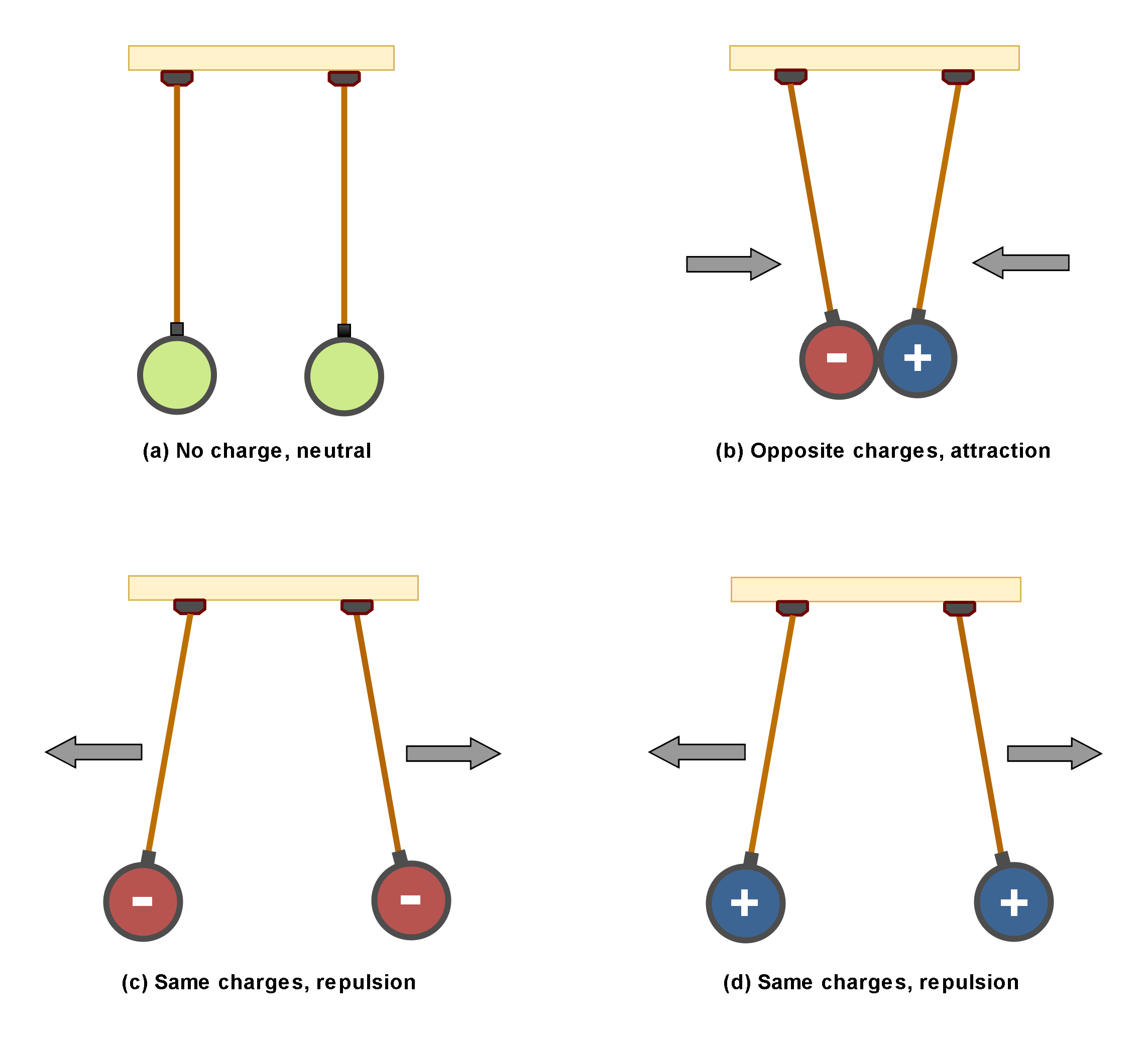
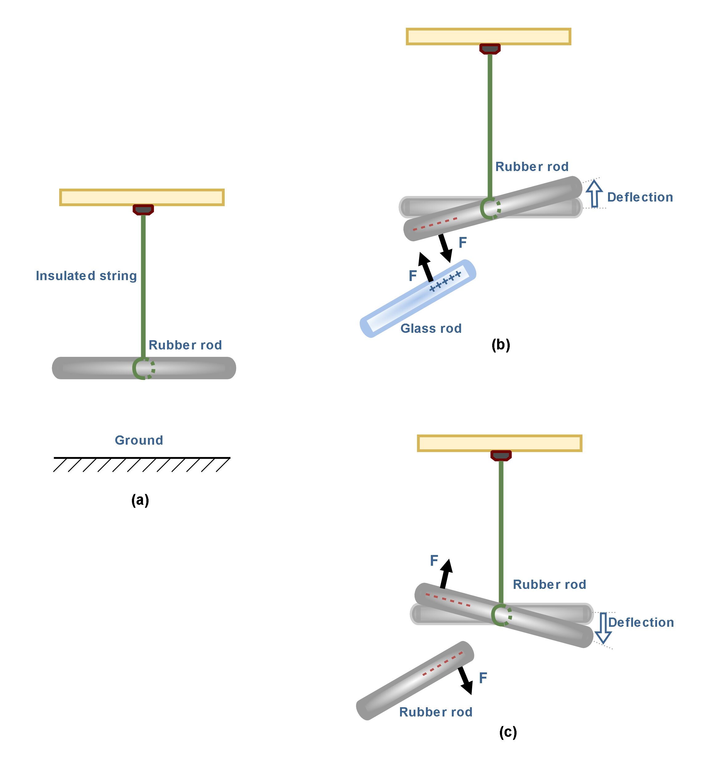
Figure 2 illustrates the interaction of two charges. There are 2 objects (for example 2 metallic spheres) suspended by insulated strings.
Figure 2: The interaction of two charges
In Figure 2(a), both of objects are uncharged and there is not any interaction between them. In Figure 2(b), they are oppositely charged and then there are attraction forces between them. This is one of the main physical principles that charges of opposite signs, attract each other.
In Figure 2(c) and 2(d), the objects are similarly charged and then there are repulsive forces between them. This is another physical fact that charges of the same signs, repel each other.
As a more realistic example, Figure 3 shows an experimental setup for observing the electrical force between two charged objects.
Figure 3: An experimental setup for observing the electrical force between two charged objects
In Figure 3(a) there is an uncharged hard rubber rod that is suspended by a piece of insulated string over the ground. We might assume that the rubber rod has already been rubbed with fur before suspending. Then, it has absorbed some negative charges. Also, we have a glass rod which has already been rubbed with silk and then it has lost some negative charges. When the positively charged glass rod is brought near the rubber rod, the rubber rod is attracted toward the glass rod because the electrostatic force between them is attractive as shown in Figure 3(b).
If two charged rubber rods (or two charged glass rods) are brought near each other, as in Figure3(c), the force between them is repulsive. These observations may be explained by assuming the rubber and glass rods have acquired different kinds of charge, where the electric charge on the glass rod is positive and that on the rubber rod is negative.
Atomic Nature Of Electricity
Atoms are the basic particles of the chemical elements. The word atom is derived from the ancient Greek word “atomos”, which means “uncuttable”.
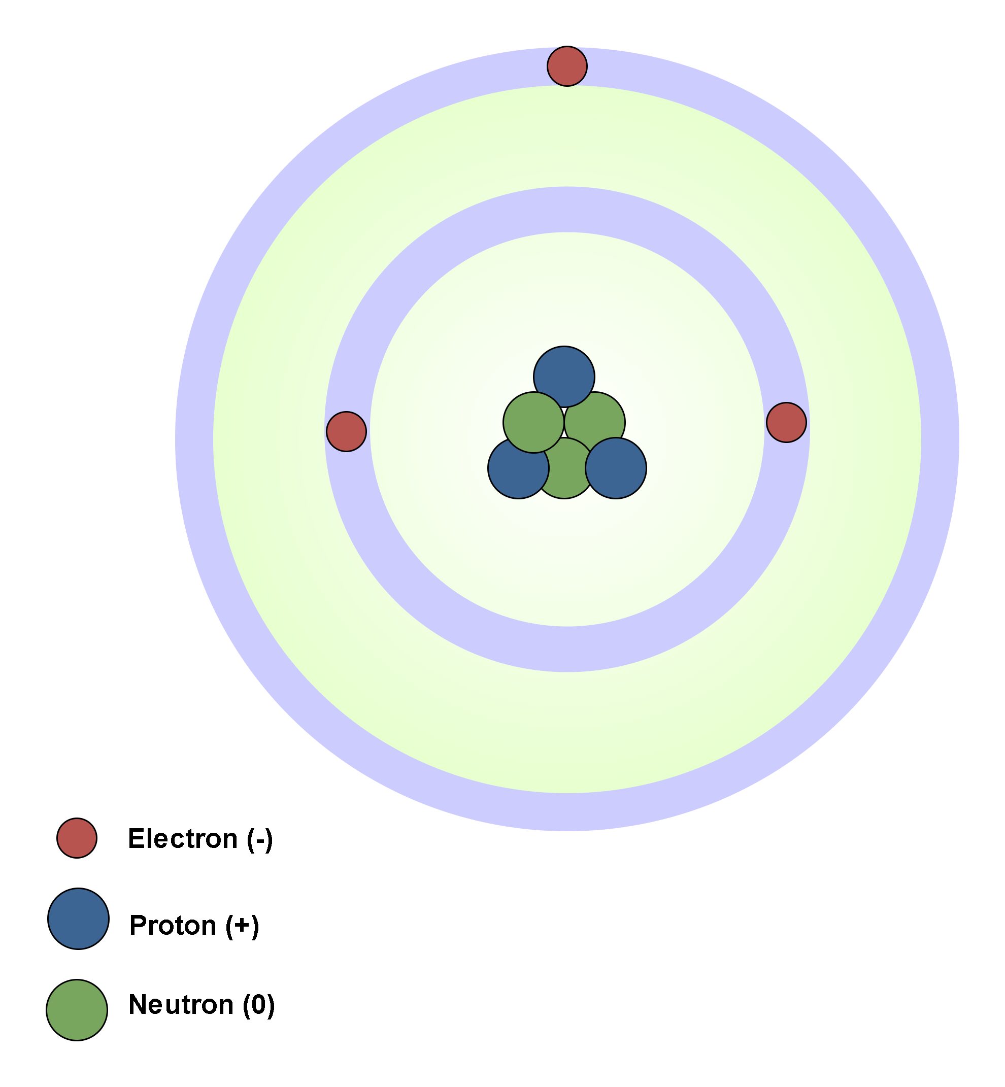
In atomic physics, the Rutherford–Bohr model of the atom, presented by Niels Bohr and Ernest Rutherford in 1913, consists of a small, dense nucleus surrounded by orbiting electrons. It is analogous to the structure of the Solar System, but with attraction provided by electrostatic force rather than gravity, and with the electron energies quantized (assuming only discrete values). Figure 4 shows the simplest classic physical model of an atom.
Figure 4: The classic physical model of an atom
Atom´s nucleus contains practically the whole mass of the atom. It consists of protons and neutrons. Neutrons are not charged. Protons are charged positively and they never move from one material to another. Electrons are small and light negatively charged that rotate around the core in electron shells. They occupy the outer regions of the atom.
In 1909 Robert Millikan (1886–1953) discovered that if an object is charged, its charge is always a multiple of a fundamental unit of charge, designated by the symbol e. Other experiments in Millikan’s time showed that the electron has a charge of -e and the proton has an equal and opposite charge of +e. In modern terms, the charge is said to be quantized, meaning that charge occurs in discrete chunks that can’t be further subdivided.
In the SI (International System of Units) the unit of electric charge is the Coulomb or C. The amount of charge of one proton is qp = +e = 1.60 × 10⁻¹⁹ C.
Table 1 provides information about particles of an atom containing the charge and mass of each component.
Table 1: The basic components of an atom
Electrons are far lighter than protons and hence more easily accelerated by forces. A typical atom contains many electrons that can be closer to or further from the core. Those further from the core are loosely bound and they can be removed by rubbing or other methods. Rubbing the two materials together serves to increase the area of contact, facilitating the transfer process.
Normally atoms are not charged. A neutral atom (an atom with no net charge) contains as many protons as electrons. Removing electrons creates a positively charged ion and placing additional electrons on the atom creates a negatively charged ion. Consequently, objects become charged by gaining or losing electrons.
Essentially, 1C is a very large amount of charge. In typical electrostatic experiments in which a rubber or glass rod is charged by friction, there is a net charge on the order of 10-6 C.
As a tangible example, an ordinary flashlight battery delivers a current that provides a total charge flow of approximately 5,000 Coulombs, which corresponds to more than 1022 electrons, before it is exhausted!
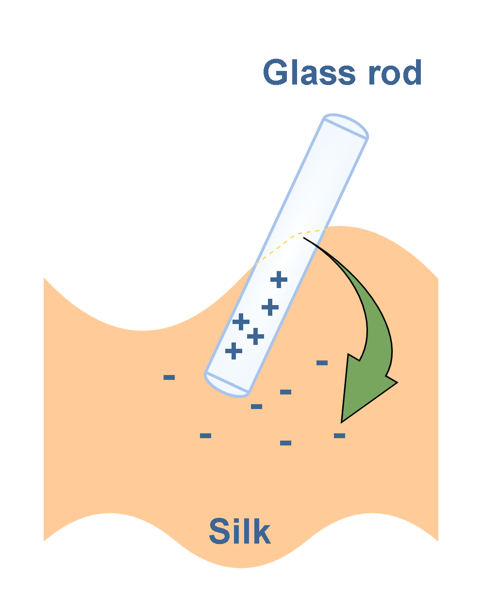
When a glass rod is rubbed with a piece of silk cloth, as in Figure 5, electrons are transferred from the rod to the silk. As a result, the glass rod carries a net positive charge and the silk carries a net negative charge.
Figure 5: Electrifying a glass rod by rubbing it with silk
The transmission of electric charges between objects, due to rubbing them together, is shown in Figure 6. If there are more protons than electrons, the object will be positively charged, and if there are more electrons than protons, it will be negatively charged. In Figure 6 (a) there are two objects without any physical contact and in the neutral state with equal amounts of positive and negative charges. In Figure 6 (b) and (c) there is physical contact between them which causes the transfer of electrons between the objects. Consequently, we have two charged objects (positively and negatively) instead of neutral ones.
Figure 6: Transferring electric charges by physical contact
Insulators And Conductors
Substances can be classified in terms of their ability to conduct electric charge. In conductors, electric charges move freely in response to an electric force. All other materials are called insulators.
Glass and rubber are insulators. When such materials are charged by rubbing, only the rubbed area becomes charged, and there is no tendency for the charge to move into other regions of the material. In contrast, materials such as copper, aluminum, and silver are good conductors. When such materials are charged in some small region, the charge readily distributes itself over the entire surface of the material.
Semiconductors are a third class of materials, and their electrical properties are somewhere between those of insulators and those of conductors. Silicon and germanium are well-known semiconductors that are widely used in the fabrication of a variety of electronic devices.
Coulomb´S Law
In 1785 Charles Coulomb experimentally established the fundamental law of electric force between two stationary charged particles. An electric force has the following properties:
The direction of the electric force is along the line connecting the charges.
The magnitude of the force F is proportional to the product of the magnitudes of the charges, q1 and q2, of the two particles.
The magnitude of the force F is inversely proportional to the square of the separation distance r, between the two charges, q1 and q2.
It is attractive if the charges are of opposite sign and repulsive if the charges have the same sign.
The force depends on the medium in which the charges are placed.
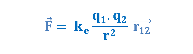
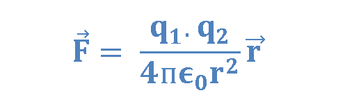
Based on his observations, Coulomb proposed the following mathematical formula for the vector electric force F between two charges q1 and q2 separated by a distance r as explained in Equation 1.
Equation 1: Coulomb’s law
where ke is a constant called the Coulomb constant. The vector electric force F involves both magnitude and direction. In Equation 1 the direction of force is governed by the unit radius vector r12 in the direction from q1 to q2. In the SI system, q1 and q2 are measured in Coulombs (C) and r in meters (m), and the force F should be Newtons (N). The value of the Coulomb constant in Equation1 depends on the choice of units. From the experiment, we know that the Coulomb constant in SI units has the value explained in Equation2.
Equation 2: Coulomb constant
Equation1, known as Coulomb’s law, applies exactly only to distinct point charges and to spherical distributions of charges, in which case r is the distance between the two centers of charges. If the force formula yields a positive value, charges repel each other. If it yields a negative value, the charges attract each other. Electric forces between stationary and unmoving charges are called electrostatic forces.
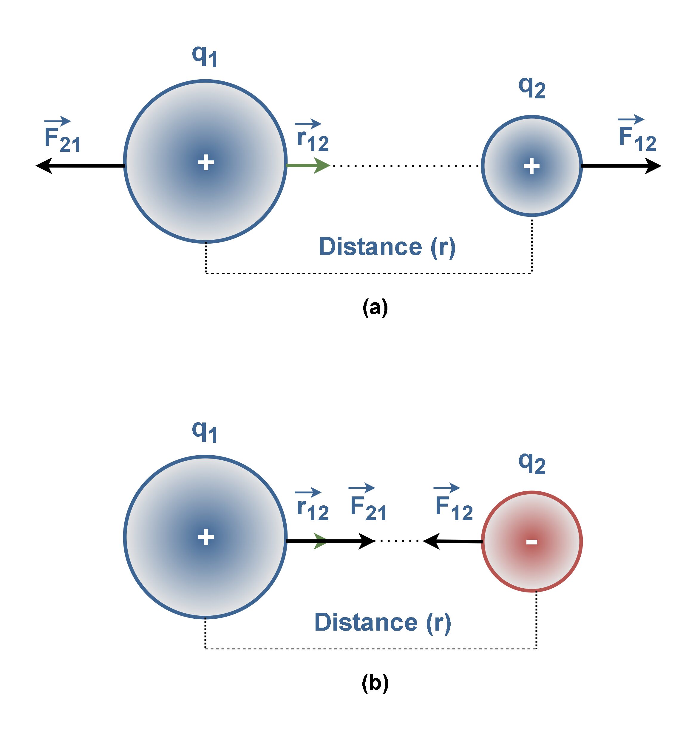
Figure 7: The electric force between two (a) similar, and (b) dissimilar sign charges
Figure 7 shows the exertion of electric forces, F12 (the force exerted by particle 1 on particle 2) and F21(the force exerted by particle 2 on particle 1) between similar-sign and dissimilar-sign q1 and q2 charges.
Figure 7(a) shows the electric force of repulsion between two positively (or two negatively) charged particles. Also Figure 7(b) shows the electric force of attraction between two opposite-sign charged particles.
Like other forces, electric forces obey Newton’s third law. Hence, the forces F12and F21are always equal in magnitude but opposite in direction, regardless of whether q1 and q2 have the same magnitude or not.
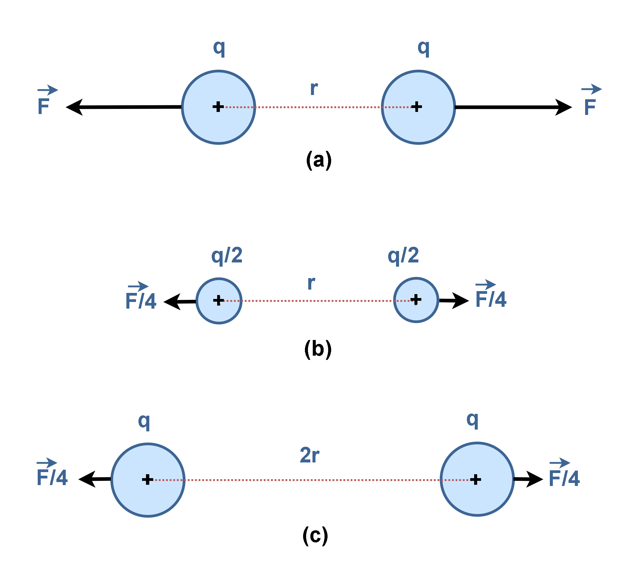
According to Equation1, if there were two positive equal charges, q, they would repel each other with the force that depends on the product (q × q) as illustrated in Figure 8(a). If each of the charges were reduced by one-half, the repulsion would be reduced to one-quarter of its former value, F/4, as depicted in Figure 8(b).
Figure 8: The effects of size and distance between charges on the electric force F
Additionally, if the distance between the two charges is doubled (2 × r), the force becomes weaker, decreasing to one-fourth of the original value (F/4), as depicted in Figure 8(c).
Another expression for the above-mentioned law is related to the definition of the permittivity (ϵ) which is a property of the medium. In the Coulomb’s law, the constant ke can also be written as Equation 3.
Equation 3: Coulomb constant
The new constant ϵ0 is called the permittivity of free space and has magnitude, measured in Farads per meter (F/m). Equation 4 defines this quantity.
Equation 4: Permittivity of free space
Thus, the Coulomb’s force law can be rewritten as Equation 5.
Equation 5: Coulomb’s law in terms of permittivity
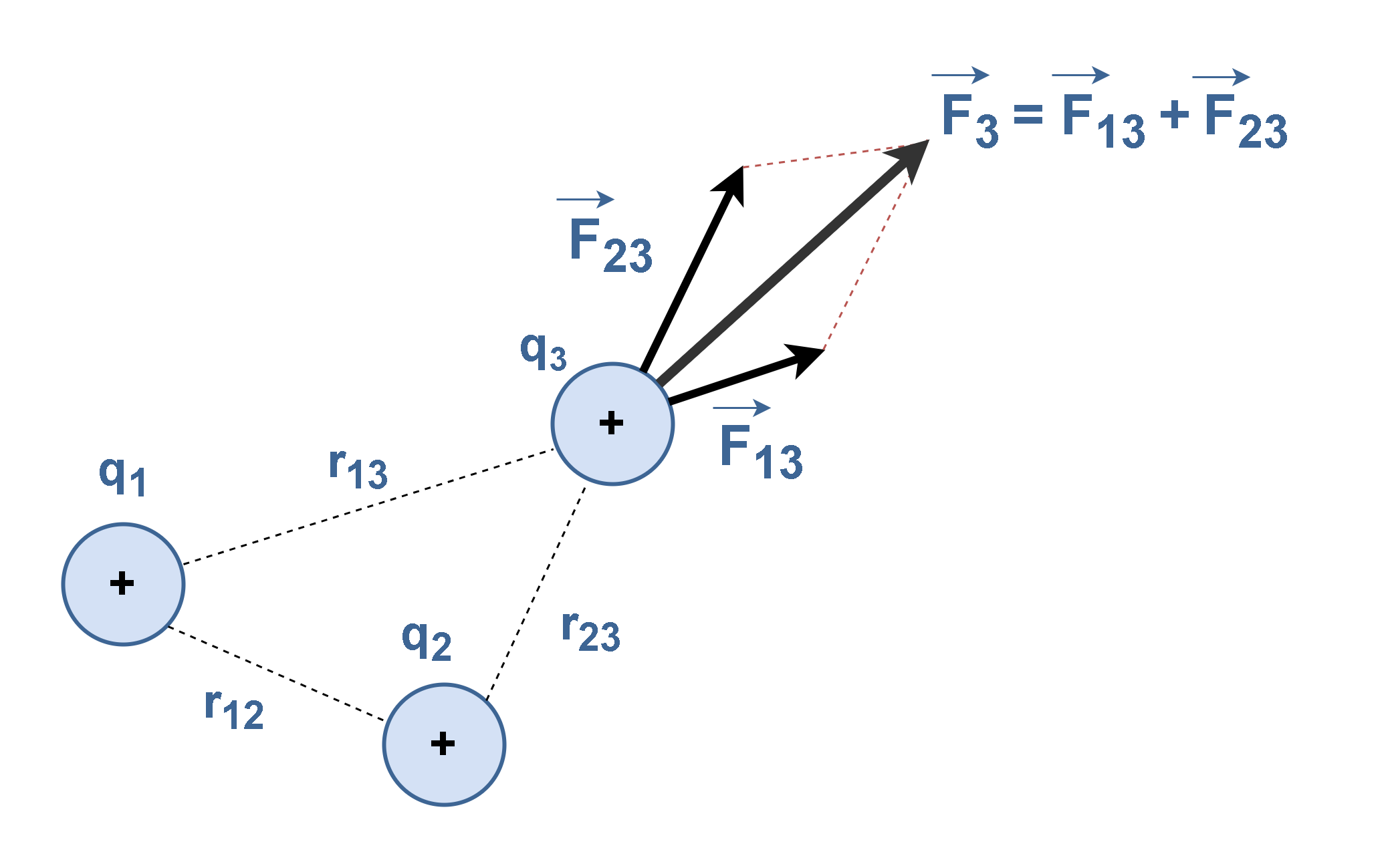
When a number of separate charges act on the charge of interest, each exerts an electric force. These electric forces can all be computed separately, one at a time, and then added as vectors. This is the superposition principle. For example, if there are several charges q1, q2 and q3, the force acting on each charge is the sum of all Coulomb forces acting on the charge from the other charges.
Figure 9 illustrates an example of the final force F3 which is the resultant of the forces exerted on q3 by q1 (F13) and by q2 (F23). Then, F3is the outcome of vector summation of F13 and F23.
Figure 9: The resultant force F3 due to the sum of forces of charges q1 and q2 on q3
Summary
Electromagnetism is the science of electric charge and of the forces and fields associated with the charge.
Electric forces are produced by electric charges either static or in motion.
Electrostatics describes electric charges at rest.
Nature’s basic carriers of positive charge are protons, which, along with neutrons, are located in the nucleus of atoms. Some particles, such as a neutrons, have no net charge.
Then, the smallest subdivision of the amount of charge that a particle can have is the charge of one proton.
The electron has a charge of the same magnitude but the opposite sign of protons.
Normally atoms are neutral as the charge of their electrons balances the charge of their core.
Electrons with negative charges can transfer readily from one type of material to another due to rubbing.
Objects usually contain equal amounts of positive and negative charge, so they are neutral. Electrical forces between objects arise when those objects have net negative or positive charges.
Like charges repel one another and unlike charges attract one another.
Different types of materials are classified as either conductors or insulators on the basis of whether charges can move freely through their constituent matter.
The SI unit of charge is the coulomb (C).
Only a very small fraction of the total available charge is transferred between the rod and the rubbing material.
When using Coulomb’s force law, remember that force F is a vector quantity and must be treated accordingly.
There are three conditions to be fulfilled for the validity of Coulomb’s law: The charges must have a spherically symmetric distribution, the charges must not overlap, the charges must be stationary.
The name “Synchronous Counter” comes from the fact that all the flip-flops inside the counter are driven through a single clock source and because of this parallel clock sourcing arrangement of flip-flops in a synchronous counter, they are often referred to as “Parallel Counters”. This indicates that with each clock pulse, the counter’s output varies concurrently and reliably. In addition to having shorter propagation latency and power usage than asynchronous counters, synchronous counters are simpler to build and evaluate. Nevertheless, they also need more wires and logic gates, which raises the circuit’s potential cost and complexity.
Synchronous counters can be built with Toggle or D-type flip-flops. In contrast to asynchronous counters, which have a direct connection between the output of the preceding stage and the clock input of the next counter stage in the chain, the synchronous counter has synchronized timing for each level. Therefore, the overall operation is faster in synchronous counters compared to asynchronous ones.
The issue with asynchronous counters is that they experience a phenomenon called “Propagation Delay,” whereby the timing signal has a slight delay as it passes through each flip-flop. On the other hand, the external clock signal is connected to the clock input of each flip-flop within the synchronous counter. This results in all the flip-flops being synchronously timed (in parallel) with each other, providing a fixed time correlation. Stated differently, the output is “synchronized” with the clock signal as it varies.
As a result of this synchronization, there is no propagation delay since every single output bit changes its state in response to the common clock signal at precisely the same moment.
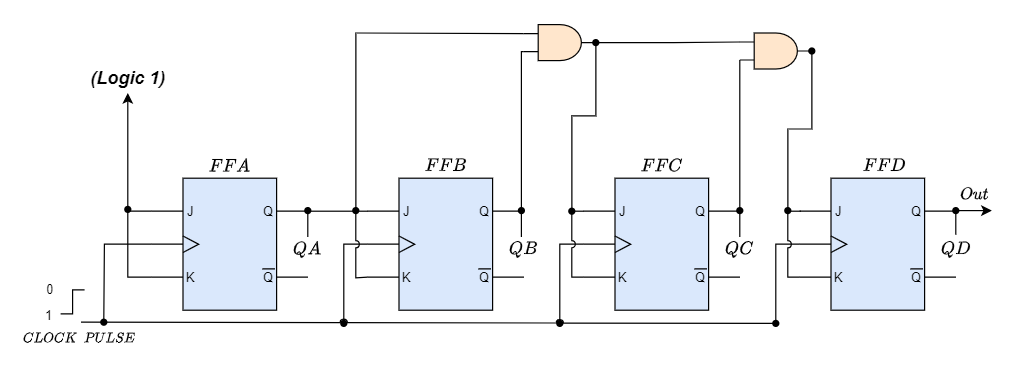
Binary 4-bit Synchronous Up Counter
Fig-1: 4-bit Synchronous Up Counter
As shown in the picture above, the JK flip-flops in the counter chain are fed by the same external clock pulses, which are meant to be counted. The J and K inputs are connected in toggle mode, but only the flip-flop FFA (LSB), which is the first flip-flop, has HIGH logic (1) connected to it, allowing it to toggle on every clock pulse. Afterward, in reaction to the common clock signal, the synchronous counter advances one state for every pulse in a predefined sequence.
The J and K inputs of flip-flop FFB are directly linked to the output “QA” of flip-flop FFA, while the J and K inputs of flip-flops FFC and FFD are driven by independent AND gates that are additionally provided with signals from the input and output of the preceding stage. The necessary logic for the JK inputs of the subsequent level is produced by these extra AND gates.
The same counting sequence as with the asynchronous circuit may be obtained if we enable each JK flip-flop to toggle depending on whether all previous flip-flops’ outputs (Q) are “HIGH.” This eliminates the ripple effect because every flip-flop in this circuit will be timed at precisely the same time.
Since all the counter stages are triggered simultaneously in parallel, synchronous counters do not have an intrinsic propagation delay, hence their maximum operating frequency is significantly higher than that of an equivalent asynchronous counter circuit.
4-bit Synchronous Counter Waveform Timing Diagram
Fig-2: Synchronous Counter Timing Diagram
The outputs of this 4-bit synchronous counter count upward from 0 (0000) to 15 (1111) because it counts consecutively on each clock pulse. As such, such kind of counter is also termed as a 4-bit Synchronous Up Counter.
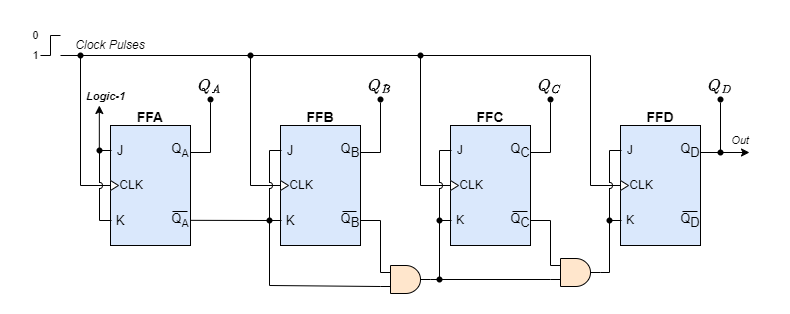
On the other hand, by connecting the AND gates to the flip-flops’ Q̅ output as demonstrated, we can quickly build a 4-bit Synchronous Down Counter and create a timing diagram that is the opposite of the one above. In this case, the counter begins with all its outputs HIGH (1111) and counts down to zero (0000) with each clock pulse application before repeating the sequence.
Binary 4-bit Synchronous Down Counter
Fig-3: 4-Bit Synchronous Down Counter
Since synchronous counters are made by joining flip-flops together, any number of flip-flops can be joined or “cascaded” together to create a binary counter that is “divide-by-n.” The modulo, or “MOD,” number remains the same as it does for asynchronous counters, allowing truncated sequences to be built alongside a Decade counter or BCD counter that has counts ranging from 0 to 2n-1. Adding an extra flip-flop and AND-gate across up or down the synchronous counter is required to enhance its MOD count.
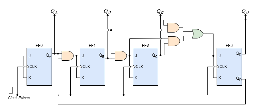
4-bit Synchronous Decade Counter
Synchronous binary counters may also be used to construct a 4-bit decade synchronous counter, which will provide a count sequence from 0 to 9. With the help of extra circuitry, a regular binary counter may be transformed into a decade (decimal 10) counter to achieve the necessary state sequence. The counter resets to “0000” whenever it reaches the number “1001”. We now have a Modulo-10 counter or decade.
Fig-4: 4-Bit Synchronous Decade Counter
When the counting sequence hits “1001” (Binary 9), which is detected by the extra AND gates, flip-flop FF3 toggles on the subsequent clock pulse. Flip-flop (FF0) toggles on and off with each clock pulse. As a result, the count restarts at”0000,” creating a synchronous decade counter.
The extra AND gates in the counter circuit above can be readily rearranged to generate other count numbers. For example, a Mod-12 counter counts 12 states from “0000” to “1011” (0 to 11) and then repeats, making it appropriate for clocks and other applications.
Triggering The Counter
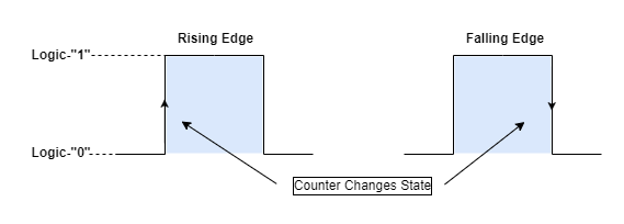
Synchronous counters employ edge-triggered flip-flops, which produce a single count when the clock input switches states on either the “positive edge” (rising edge) or the “negative edge” (falling edge) of the clock pulse on the control input.
Synchronous counters typically count on the rising edge of the clock signal, which is the transition from low to high, whereas asynchronous ripple counters count on the falling edge, which is the transition from high to low.
Fig-5: Counter State Change
The most significant bit (MSB) of one counter can control the clock input of the next stage flip-flop, which makes it easier to link counters together even if it may seem strange since ripple counters utilize the clock cycle’s “falling edge” to change states.
This can function because a carry to the next bit must happen at the time when the preceding bit goes from high to low. To connect counters without causing any propagation delays, synchronous counters often have a carry-out and a carry-in pin.
Applications of Synchronous Counters
Digital circuits used in embedded systems, automotive systems, and consumer electronics are all built with synchronous counters. They have precise timekeeping capabilities and drive time displays in forms like hours, minutes, and seconds.
In Arithmetic Logic Units (ALUs), synchronous counters are employed to carry out addition, subtraction, multiplication, and division operations on binary integers. In computation-intensive applications and digital signal processing, they help to efficiently implement digital arithmetic algorithms.
In digital systems, synchronous counters are essentially required for producing accurate timing signals and managing the order of processes. They are utilized in timing generators to produce clock signals with precise frequencies and duty cycles, as well as in synchronization circuits to guarantee synchronized activities among various system components.
They are useful in industrial automation operations, where synchronous counters are used in situations where precise counting of events or occurrences is required. This might include keeping track of the frequency of transmissions in communication systems or counting the pulses in sensor systems.
Advantages:
The Synchronous counter operates faster as they are not accompanying any propagation delay.
Error probabilities decreased because logic gates regulate the count sequence.
synchronous counters are more suitable for high-speed and accurate operations, such as frequency division, binary arithmetic, and digital clocks.
Synchronous counters can easily be modified and extended to create different types of counters, such as up-down, modulo-n, and ring counters.
Disadvantages:
The circuit gets increasingly complex as the number of states rises.
An asynchronous counter has a single common clock pulse that drives all its flip-flops.
When compared to asynchronous counters, they require more hardware and components.
Synchronous counters can consume more power than asynchronous counters since they have more logic gates and wiring that draw current.
Conclusion
Synchronous counters operate using a single clock signal to drive all flip-flops within the counter, simultaneously. This ensures that all the outputs are synchronized with the clock signal, eliminating propagation delays present in asynchronous counters.
D-type or Toggle flip-flops can be used to create synchronous counters.
Synchronous counters can be used for the construction of modular counters, including decade counters that count from 0 to 9. These counters reset after reaching the maximum count, achieved through additional circuitry.
Logic gates are used to regulate the count sequence.
Compared to asynchronous counters, synchronous counters are simpler to construct.
It is possible to get an overall speedier operation as compared to asynchronous counters.
Synchronous counters are more suitable for high-speed and accurate operations, such as frequency division, binary arithmetic, and digital clocks.
So you’ve just finished designing your new PCB, completed all ERC and DRC checks, and sent the files off to the manufacturer. Now, you’re eagerly awaiting the arrival of your new PCBs. If you’re like me, once you’ve generated your Gerber files, you head to an online Gerber viewer site like PCBWay or JLCPCB to inspect your PCBs for any additional aesthetic errors and then send them off to your manufacturers.
But what if I tell you there’s a better way to check your Gerber files which will give you various additional analysis tools to get those sneaky errors out of your design? That’s where NextPCB’s Free Gerber Viewer (HQDFM) comes in. Gerber files are the standard in PCB design, containing crucial data for manufacturers. Analyzing them can be complex, but HQDFM’s software simplifies the process, offering a user-friendly interface and resources, designers can ensure manufacturability and spot errors efficiently.
What Does DFM Stand for and Why It’s Important?
DFM stands for “Design for Manufacturability” or “Design for Manufacturing.” It’s an engineering approach that focuses on designing products in a way that makes them easier and more efficient to manufacture. DFM aims to streamline the manufacturing process, reduce costs, improve quality, and shorten time to market by considering manufacturing constraints and requirements during the design phase.
In a practical term we check for Tracewidth/spacing, Drill hole/slot sizes, Clearances to copper and board, Layer to Layer drill holes, solder mask openings, silk screen errors, and more.
What is HQDFM and What is so Special About it?
HQDFM is NextPCB’s Free Gerber Viewer tool It is a powerful and user-friendly tool that supports Gerber X2, RS-274X, and ODB++ file formats. With zoom, pan, and measurement tools, ensure quality and integrity in your PCB designs. Seamlessly compatible with Altium, Eagle, and KiCad, it offers advanced features like layer selection and transparency control for detailed analysis. Once you download the tool you need to create your own free account and log in to work with this tool.
The tool is easy to use, once installed just drag and drop the Gerber and it gets uploaded to the software, it also features a One-click PCB file checker for quick analysis and generates a report through which you can analyze the PCB. On top of that penalization, impedance calculator, routing distance calculator, and more features make the diagnosis process easier. It can also generate BOM and coordinate files to order the PCB from the next website. The tool is completely free and can be used by anyone.
How to Use the HQDFM Tool
To begin using the Design for Manufacturability (DFM) tool, import your Gerber file, and you also need to import your BOM file if you are willing to check a new window will open for that. Now click on the “DFM Analysis” A detailed analysis of your PCB will start presenting results for PCB and PCBA analyses. Now you can correct any design errors based on these results to prevent real-life issues. You will get an estimated price of 5 quantities of your PCB and expected making time.
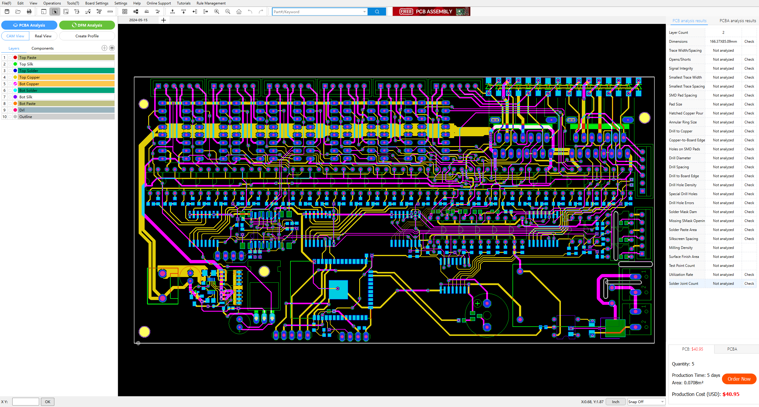
All Layer View in HQDFM
The DFM analysis section offers CAM view, Real View, and profile creation as an added option. It includes layer and component lists for PCB inspection. The tools section in the menu bar provides additional features like an impedance calculator, file comparison, copper area calculation, and more.
BOM and centroid file checker
One of the most powerful features of this tool is the BOM and centroid file checker, the HQDFM identifies inconsistencies in BOM and Centroid files, which are hard to detect manually and can lead to confusion during assembly. It checks for quantity mismatches, duplicate entries, and incorrect part values, saving engineers from tedious manual review tasks. HQDFM also checks whether all the parts in the BOM are present in the centroid data system, which may be a result of poor version control setup.
Footprint Checker
The new update includes a powerful footprint checker that compares PCB design land patterns with the expanding HQDFM database. With a single click, it checks over half of the BOM parts and offers immediate feedback on problematic patterns. There is also the option for the Users can expand the database or manage a local one.
DFA analysis
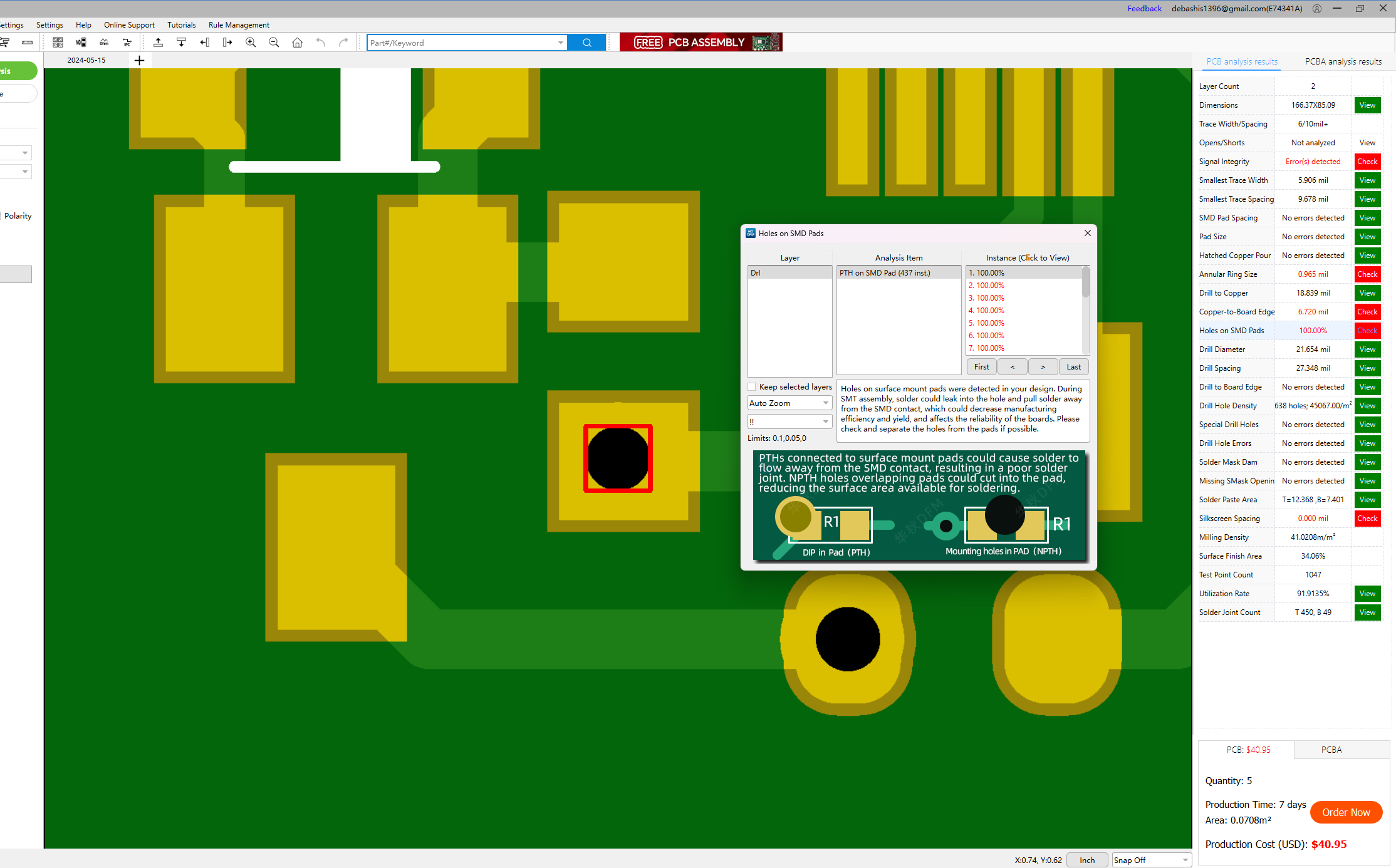
DFA Found Misplaced VIA on the PCB
HQDFM’s DFA checks utilize component and x-y coordinate data to simulate accurate component placement, even without existing footprint data. It includes checks for pad size, hole diameter and placement, component clearances, pad contact areas, and PCB shadowing. Based on IPC guidelines and real assembly data, HQDFM’s generic feedback benefits all PCB layout engineers by focusing on general industry capabilities rather than specific assembler processes.
The new HQDFM additions offer significant verification checks for PCB design, addressing commonly encountered assembly problems. This free software educates designers and provides early resolution tools. Download the updated HQDFM suite from the official HQ Electronics (NextPCB) website. A free online Gerber Viewer version is also available for new users or non-Windows users needing bare PCB DFM features.
You may also find interesting (Promo offers):
Free assembly for 5 pieces PCBA: For free PCB assembly, no coupon code or application is required. Just go to the PCB assembly order page and follow the step-by-step instructions. If your order fulfills the free assembly conditions, the assembly, setup and operation fees will automatically be deducted on the spot and you only pay for the PCB, components and shipping. The free assembly offer can be used multiple times.
50% off Batch PCB Assembly from HQ NextPCB: All users who log into their HQ Electronics account will receive a 50% off PCB assembly coupon. To use it, add the qualifying order to your shopping basket and select the coupon at the checkout. The coupon can only be used once (The coupon can be found in your account after logging in).
NextPCB offers the best value for money in the market with rich capabilities, quality, speed, and customer service. Whether you are developing a new product or a one-off project, there is no excuse not to give us a try. Visit the PCBA order page or try the links below to get started.
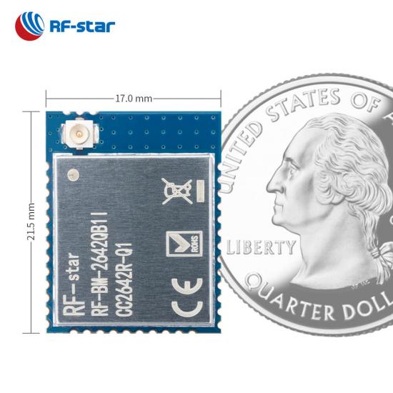
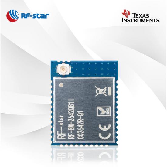
RF-star, a leading manufacturer of wireless modules and provider of wireless connectivity solutions, proudly announces the expansion of its Bluetooth module lineup tailored specifically for automotive applications. The latest BLE modules include the RF-BM-2642QB1I and RF-BM-2340QB1, designed to excel in automobile-critical applications such as digital car keys, T-Box, Tire Pressure Monitoring Systems (TPMS), Passive Entry Passive Start (PEPS), and more.
Designed to meet the evolving demands of the automotive industry, RF-star’s new modules offer a host of features to enhance reliability, durability, security, and ease of integration.
Compliance and security assurance are paramount in automotive applications
RF-star’s new Bluetooth Low Energy modules are based on TI chips, specifically the CC2642R-Q1 and CC2340R5-Q1 MCUs meeting Automotive Electronics Council (AEC-Q100) standards. RF-BM-2642QB1I and RF-BM-2340QB1 BLE modules integrated with the automotive-qualified MCUs can operate in Grade 2 temperature range (–40 °C to +105 °C), guaranteeing their reliability and durability in harsh automotive environments.
Additionally, RF-star’s CC2642R-Q1 and CC2340R5-Q1 modules incorporate AES 128-and 256-bit cryptographic accelerator, ECC and RSA public key hardware accelerator and true random number generator(TRNG). These advanced security enablers with robust encryption protocols and authentication mechanisms, provide peace of mind to both automakers and end-users.
Rich resources and ease of use are also taken into consideration by project decision-makers
Their high-performance processor and abundant resources, eg., RF-BM-2340QB1 with 512 kB Flash and 36 kB RAM, offer ample opportunities for firmware development. Meanwhile, they also support over-the-air upgrade (OTA).
Besides, the automotive modules feature UART, SPI, I2C, I2S, ADC and more digital peripherals, flexible RF output modes(eg., PCB antenna, IPEX connector and half-hole ANT RF pin), and user-friendly development kits. Hence, it is quite easy to integrate into existing vehicle architectures, especially the auto aftermarket applications.
Best of all, both support Bluetooth 5.0 Low Energy serial port transmission for master-slave wireless connections. These rich functions with AT commands streamline the integration process, reducing complexity and accelerating time-to-market for automotive projects. Whether experienced engineers or newcomers to wireless connectivity, they can leverage RF-star’s Bluetooth modules easily to unlock their full potential in ongoing projects.
RF-star – A powerful supplier with abundant experience stands out among competitors
Certified with ISO9001 and IATF16949 (automotive sector quality management systems), the enterprise and the manufacturer meticulously adhere to international quality management standards. RF-star is also honored as a member of the Car Connectivity Consortium (CCC) and Intelligent Car Connectivity Industry Ecosystem Alliance (ICCE).
Beyond indispensable compliance, RF-star has an innovative and professional development team. With over a decade of hands-on experience in manufacturing wireless modules, RF-star earns a high reputation from domestic and overseas customers based on the supply capacity of KK-level OEMs, reliable quality and expert service.
“We are thrilled to introduce our latest BLE modules tailored for automotive applications,” said King Kang, CEO of RF-star. “With the CC2642R-Q1 and CC2340R5-Q1 modules, we aim to empower automakers with robust, secure, and easy-to-integrate solutions that enhance connectivity and user experience in modern vehicles.”
RF-star’s RF-BM-2642QB1I and RF-BM-2340QB1 Bluetooth modules are in stock and ready for immediate shipment. For more information about the automotive BLE modules, please visit www.rfstariot.com.
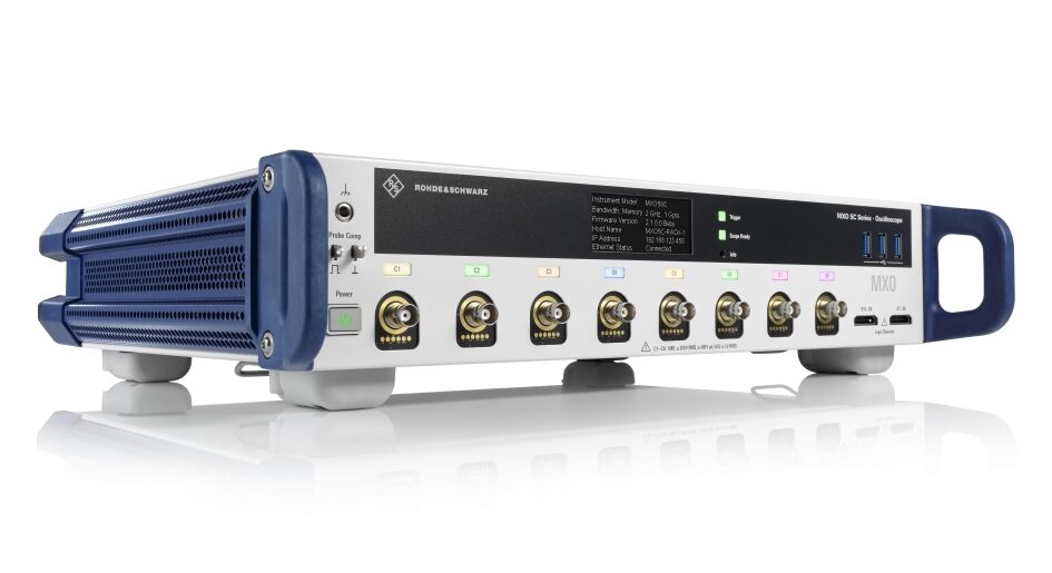
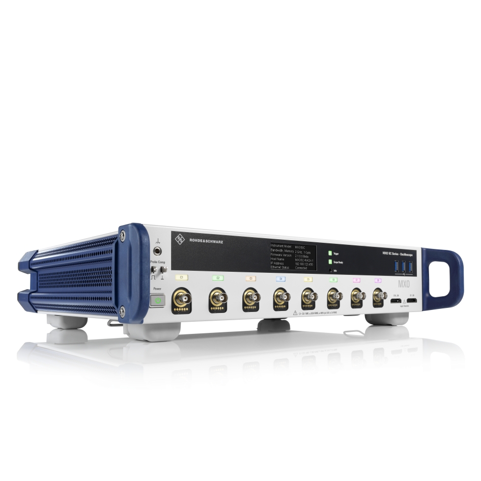
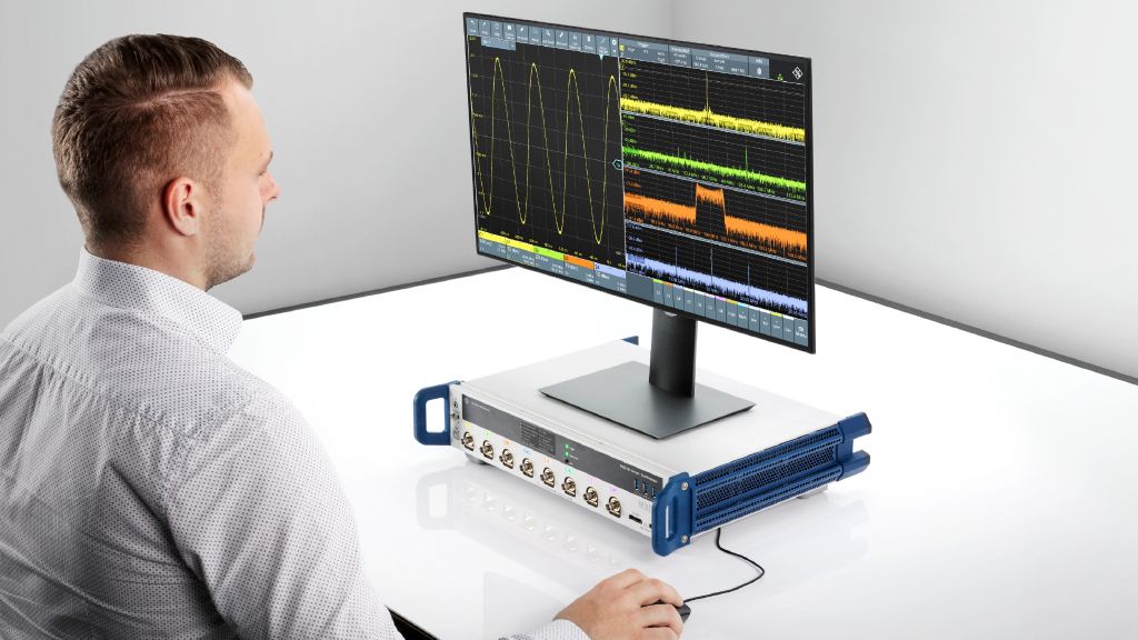
Rohde & Schwarz extends its portfolio with a 2U high oscilloscope/digitizer tailored for rack mount and other applications where a low-profile form factor is critical. The new MXO 5C series is the company’s first oscilloscope without an integrated display. It delivers the same peformance as the previously introduced MXO 5 series, but with a fourth of the vertical height.
Rohde & Schwarz introduces the new MXO 5C oscilloscope with four or eight channels. The new series is based on the next-generation MXO 5 oscilloscope and specifically addresses rack mount and automated test system applications where users are often confronted with space limitations. The instrument’s 2U vertical height – just 3.5” or 8.9 cm – allows engineers to deploy it in test systems where a traditional oscilloscope with a large display would not fit. The compact form factor is also of value in applications with high channel density where users need a large number of channels in a small volume. Users operate the instrument via the integrated web interface, or they interact with it exclusively programmatically and use the instrument as a high-speed digitizer.
Like other MXO oscilloscopes, the new MXO 5C series builds on next-generation MXO-EP processing ASIC technology developed by Rohde & Schwarz. It offers the fastest acquisition capture rate in the world of up to 4.5 million acquisitions per second. This makes it the world’s first compact oscilloscope that allows engineers to capture up to 99% real-time signal activity enabling them to see more signal details and infrequent events better than with any other oscilloscope.
Philip Diegmann, Vice President Oscilloscopes at Rohde & Schwarz, said:
“While oscilloscopes with large displays work well for bench usage, we’ve had a number of customers ask for a version that is tailored for rack mount applications. At the same time, we have customers who need a large channel count, for example in physics. With the MXO 5C we created a unique instrument that offers the best possible performance for both scenarios.”
The new form factor allows to place many channels in close proximity. The eight-channel model of the MXO 5C provides a channel density of 1500 cm3 per channel and consumes just 23 watts per channel.
While primarily designed for rack mount usage, the instrument doubles as a stand-alone bench oscilloscope. Users can simply attach an external display via the built-in DisplayPort and HDMI connectors, or they can access the instrument’s GUI via a web interface by typing in the oscilloscope’s IP address into their browser. As the first oscilloscope to offer E-ink display technology, the MXO 5C shows the IP address and other critical information on a small non-volatile display on the front of instrument, which stays visible even when power is switched off.
Like the MXO 5, the MXO 5C series comes in both four and eight channel models, in bandwidth ranges with100 MHz, 200 MHz, 350 MHz, 500 MHz, 1 GHz, and 2 GHz models. The starting price of EUR 18 000 for the eight-channel models sets a new industry standard. Various upgrade options are available to users with demanding application needs, such as 16 digital channels with a mixed-signal oscilloscope (MSO) option, an integrated dual-channel 100 MHz arbitrary generator, protocol decode and triggering options for industry-standard buses and a frequency response analyzer to enhance the capabilities of the instrument.
The new MXO 5C series oscilloscopes are now available from Rohde & Schwarz and selected distribution channel partners. For more information on the instrument, visit : https://www.rohde-schwarz.com/product/MXO5C
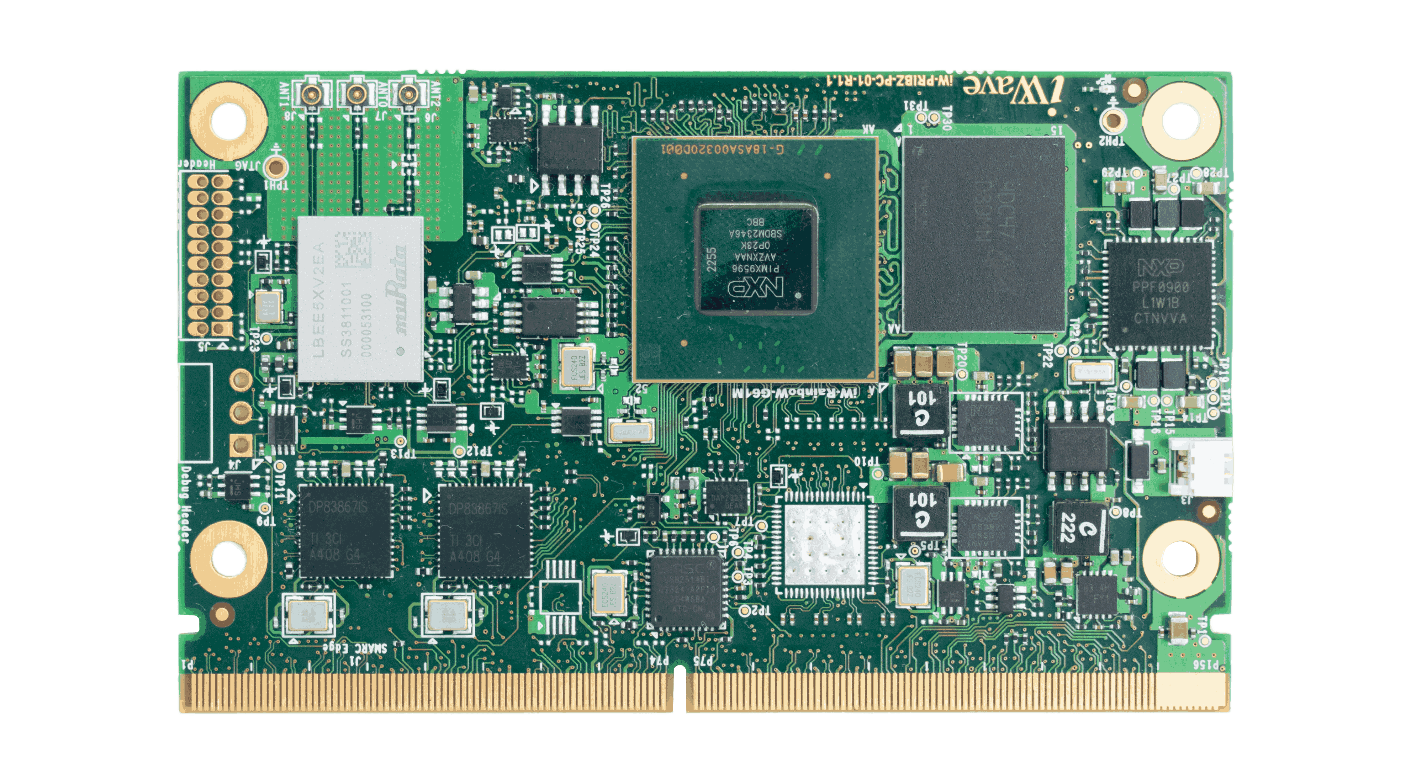
The SoM helps you leverage the multi-core architecture of the NXP i.MX 95 applications processor family, offering high-speed data processing alongside secure, real-time, and low-power modes. The SoM offers high-speed connectivity options such as 10GbE, USB 3, PCIe® Gen 3, together with Wi-Fi 6 and Bluetooth 5.3 wireless connectivity. The System on Module caters to a wide range of products and applications ranging from automotive connectivity and infotainment systems to Industry 4.0 applications.
The flex domains on the NXP i.MX 95 SoC allows engineers to mix which pieces of IP they want to use in a particular domain. The Multimedia block includes an Arm Mali 3D GPU core, but also an independent 2D GPU with a real-time blend engine. The i.MX 95 SoC is also NXP’s first applications processor to support LPDDR5 DRAM, enabling increased bandwidth for applications leveraging the embedded workload accelerators
Key features of iW-RainboW-G61M:
NXP i.MX 95 applications processor
6 x Cortex-A55 @ up to 2GHz
1 x M33 core @333MHz
1 x M7 core @800MHz
eIQ® Neutron NPU up to 2.0 TOPS
16GB LPDDR5
16Mb QSPI Flash and
16GB eMMC Flash
Wi-Fi 6 & BT 5.3 Connectivity
2x LVDS, 1x MIPI CSI, 1x HDMI
2x Gigabit Ethernet, 2x PCIe 3.0
4x USB 2.0 Host, 1x USB 3.0 OTG
1x SerDes (10G), 2x CAN, 3x I2C, 1x SD (4bit)
SMARC v2.1.1 Standard (82mm x 50mm)
Linux 6.6 BSP Support
MX 95 SAMRC PR image
The SoM is available in Industrial Grade with the associated BSP support and regular software updates from iWave. iWave assures customers a SoM product longevity of 15+ years and complementary ODM models on hardware customization, software customization, and mechanical and thermal analysis.
“iWave is excited to launch the iW-RainboW-G61M System on Module in Embedded World 2024, offering designers a powerful SoC with advanced 3D graphics, neural processing, and a new flex domain architecture, “said Immanuel Rathinam, Vice President – System on Modules at iWave. As a premier partner with early access to NXP technology, iWave iW-RainboW-G61M System on Module, powered by the NXP i.MX 95 applications processor, enables customers to leverage the powerful features of the latest SoC from NXP.”
“The NXP i.MX 95 is designed to deliver the next generation of edge computing performance for the industrial IoT market;” stated Robert Thompson, Director, Secure Connected Edge ecosystem, NXP. “iWave has a long history of developing advanced system on modules based on NXP’s i.MX applications processors. The iW-RainboW-G61M not only extends this collaboration but delivers the features of the i.MX 95 in a module that will accelerate time to market for customers.”
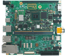
Complementing our System on Module, iWave enables customers with NXP i.MX 95 SoM evaluation kits with the latest software packages to expedite their evaluation and time to market.
Evaluation Kit Features:
2x Gigabit Ethernet Jack
1x PCIe port & M.2 KEY B PCIe
2x USB 2.0 Host Type-A, 1x USB 2.0 OTG Type microAB
USB 3.0 Host Type-A/ Type-C OTG
1x Standard SD
HDMI-Type A Connector
20pin LVDS Connector
MIPI CSI Camera Connector
2x Audio In & Out Jack through I2S Codec
2x CAN Header
MX 95 SAMRC Development kit image
Click here for more details on the NXP i.MX 95-based System on Module and Evaluation Kit.