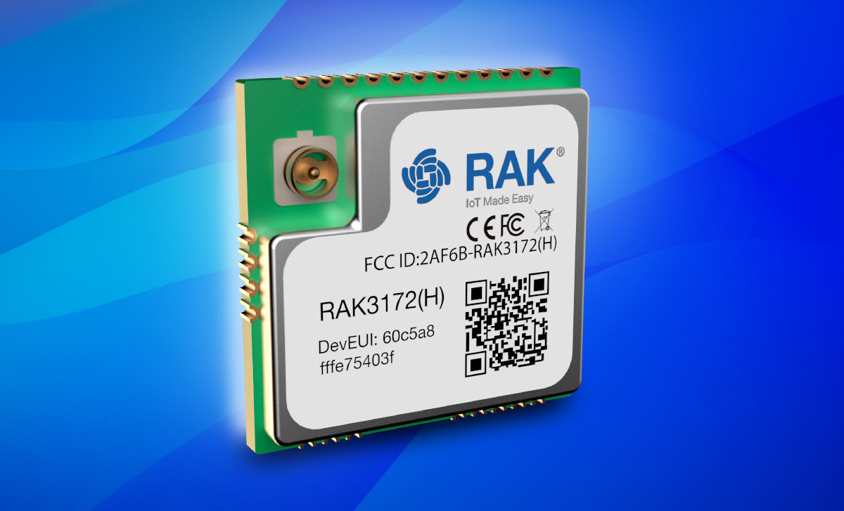
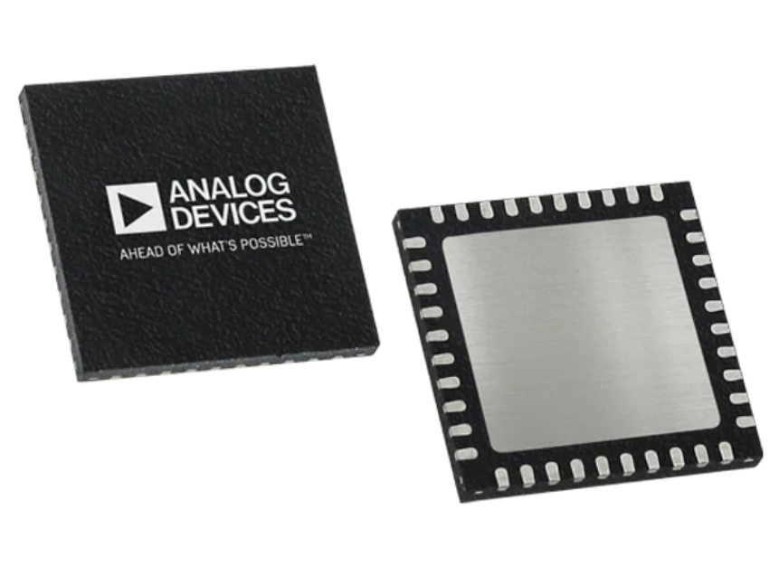
The RAK3172 LoRa Module includes a STM32WLE5CC chip, which supports eight (8) spreading factors (SF5 ~ SF12) and signal bandwidth that can be adjusted between 7.8 kHz to 500 kHz. It has Ultra-Low Power Consumption of 1.69 μA in sleep mode, but during the Transmit Mode, it can reach the maximum output power of 22 dBm. As a receiver, it can achieve a sensitivity of -148 dBm.
The module complies with Class A, ClassB, Class C of LoRaWAN 1.0.3 specifications, and it also supports LoRa Point to Point (P2P) communications. The module is suitable for various applications that require long-range data acquisition and low power consumption, such as smart meters, supply chain and logistics tracking, agricultural sensors, and smart cities.
You can configure the mode and operation of the RAK3172 module using RAK3172 AT Commands via a UART interface. Also, it offers low-power features that are very suitable for battery-powered applications.
Product Features
LoRa module for Smart City, Smart Agriculture, Smart Industry
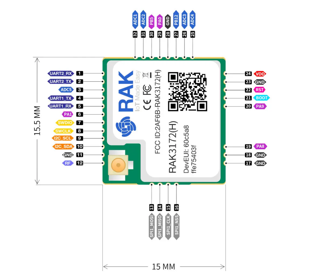
Compact Form Factor: 15 x 15.5 x 3.5 mm 32 Pin Stamp Pad for PCB SMT mounting I/O ports: UART/I2C/SPI/ADC/GPIO
Temperature range: -35 °C to +85 °C
Supply voltage: 2.0 ~ 3.6 V
Frequency range: 150 MHz to 960 MHz
Low-Power Wireless Systems with 7.8 kHz to 500 kHz Bandwidth
Ultra-Low Power Consumption 1.69 μA in sleep mode
Core: ARM 32-bit Cortex – M4 with MPU Up to 256 KB flash memory with ECC
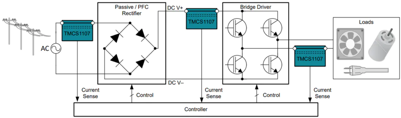
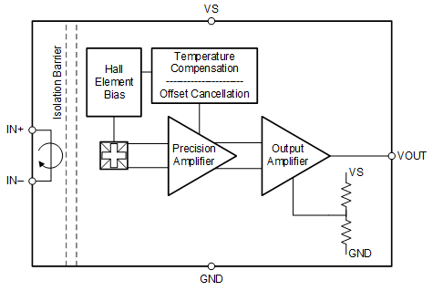
Texas Instruments TMCS1107 Hall-Effect Current Sensor is a galvanically isolated Hall-effect current sensor capable of DC or AC current measurement with high accuracy, excellent linearity, and temperature stability. A low-drift, temperature-compensated signal chain provides < 3% full-scale error across the device temperature range.
The input current flows through an internal 1.8mΩ conductor that generates a magnetic field measured by an integrated Hall-effect sensor. This structure eliminates external concentrators and simplifies design. A low conductor resistance minimizes power loss and thermal dissipation. Inherent galvanic insulation provides a 420V lifetime working voltage and 3kVRMS basic isolation between the current path and circuitry. Integrated electrical shielding enables excellent common-mode rejection and transient immunity.
The output voltage is proportional to the input current with multiple sensitivity options. Fixed sensitivity allows the TMCS1107 to operate from a single 3V to 5.5V power supply, eliminates ratiometry errors, and improves supply noise rejection. The current polarity is considered positive when flowing into the positive input pin. Both unidirectional and bidirectional sensing variants are available. The Texas Instruments TMCS1107 draws a maximum supply current of 6mA, and all sensitivity options are specified over the operating temperature range of –40°C to +125°C.
System Diagram
Features
±1% typical, ±3% maximum, –40°C to 125°C total error
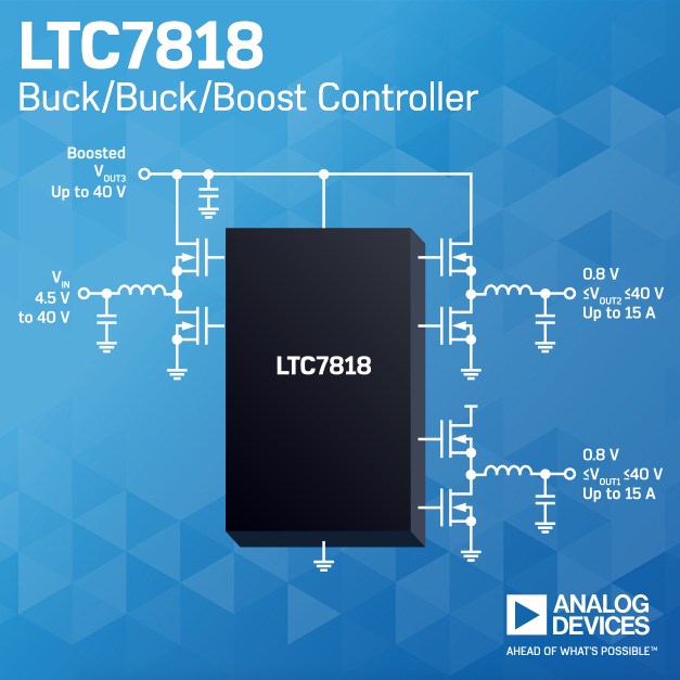
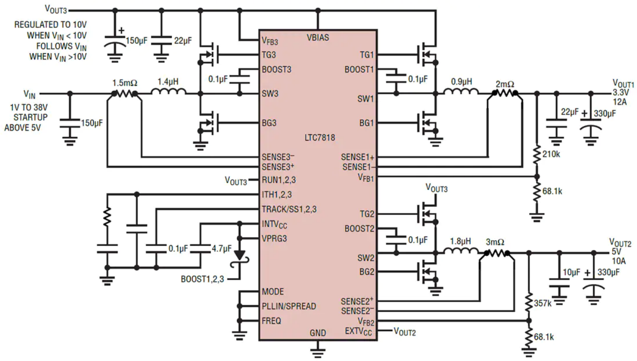
Analog Devices LTC7818 Triple Output Synchronous Controllers are high-performance synchronous DC/DC switching regulator controllers that drive all N-channel power MOSFET stages. Its constant frequency current mode architecture allows a phase-lockable switching frequency of up to 3MHz. The LTC7818 operates from a wide 4.5V to 40V input supply range. When biased from the output of the boost converter or another auxiliary supply, the LTC7818 can operate from an input supply as low as 1V after start-up.
The very low no-load quiescent current extends operating run time in battery-powered systems. OPTI-LOOP® compensation allows the transient response to be optimized over a wide range of output capacitance and ESR values. The LTC7818 features a precision 0.8V reference for the bucks, 1.2V reference for the boost, and a power-good output indicator. The LTC7818 additionally features spread-spectrum operation which significantly reduces the peak radiated and conducted noise on both the input and output supplies, making it easier to comply with electromagnetic interference (EMI) standards.
Application Diagram
Package
Features
Dual buck plus single boost synchronous controllers
Low operating IQ
14μA (14V to 3.3V, channel 1 on)
Outputs remain in regulation through cold crank down to 1V input supply voltage
4.5V to 40V wide bias input voltage range
Buck and boost output voltages up to 40V
Spread spectrum operation
RSENSE or DCR current sensing
100% duty cycle for boost synchronous MOSFET
Programmable fixed frequency (100kHz to 3MHz)
Phase-lockable frequency (100kHz to 3MHz)
Selectable continuous, pulse-skipping, or low ripple burst mode operation at light loads
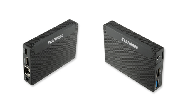
We have already seen Firefly’s RK3566-based mini-computer that was designed to compete with the powerful Raspberry Pi 4. With support from the community, Firefly has now released a new mini-PC, Station M2 based on the high performance, low power powerful Rockchip SoC, RK3566 that can now run Linux or Android. The board also supports 8GB RAM and 128GB eMMC storage for the user to play high-end applications on this tiny mini-PC.
The SoC features a quad-core 64-bit Cortex-A55 processor, clocked up to 1.8 GHz frequency along with the Mali-G52 GPU. The ultra-compact mini-PC is a successor to their Station M1 mini-PC that was launched last year and built around Rockchip’s RK3328. The station M1 was not as powerful as this release as it came with only 2GB/4GB RAM and 16GB storage.
Some of the key upgrades to Station M2 include the addition of an M.2 2242 slot for NVMe SSDs and also support more SPI flash storage of up to 16M. In terms of wireless connectivity, the Station M2 gets faster dual-band Wi-Fi 802.11 with Bluetooth 5.0. Also, as mentioned earlier, the successor Station M2 now comes with a configuration of 8GB/128GB.
Features:
CPU: Rockchip RK3356 22nm fabricated SoC featuring a quad-core 64-bit Cortex-A55 processor, clocked up to 1.8 GHz
Wireless Connectivity: Wi-Fi 802.11a/b/g/n, Bluetooth 5.0
Interfaces: HDMI 2.0, USB 3.0, USB 2.0, MIPI DSI, MIPI CSI, SPI, I2C, UART, ADC, PWM, GPIO, PCIe, I2S.
OS Support: Android 11.0, Ubuntu 18.04, Buildroot + QT, Station OS
Size: 93.8mm x 65.0mm x 15.8mm
Power: 5V via Type-C port
The Station M2 mini-PC interestingly supports several OS including the Station OS that offers a variety of applications and seamless switching between the desktop and media modes. Along with this, the hardware also supports Android 11.0 and Ubuntu 18.04 which is the most stable Linux Distro. With HDMI 2.0 onboard, users can take advantage and live stream video files using video decoding H.265 and 8GB RAM.
The mini-PC is now up for sale at $79 for 2GB/32GB, $105 for 4GB/32GB, and $149 for 8GB/64GB variant. Head to the product page for more hardware specifications.
For real-time AI applications, it is important to process incoming data using a trained neural network model. For faster data processing, the introduction to AI inference at cloud did support many aspects, increasing efficiency, but the need to process the data at the end device has become vital. To serve this purpose, we have AI inference at the edge. With AI inference at the edge, the market for real-time data processing and obtaining quick results has increased performance. When it comes to AI inference at the edge, several ASICs in the market are custom-built for this purpose. Google introduced an Edge TPU application-specific integrated circuit designed to run inference at the edge.
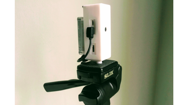
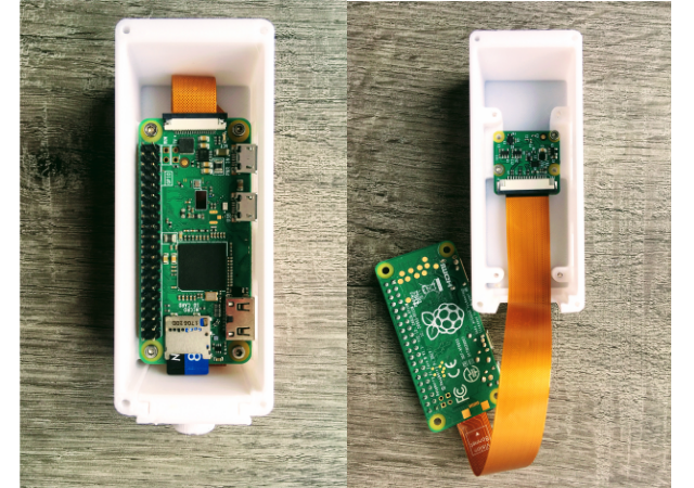
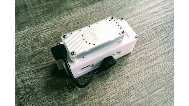
There have been several designs using Google’s Edge TPU, but this specific project, Maple Syrup Pi Camera, an AIoT smart camera has caught the eye of the makers’ community due to its use of Raspberry Pi Zero W for AI inference at the edge. We don’t usually see these SBCs used to run inference at the edge due to their low processing capabilities. For specific AI purposes, we have several powerful SBCs in the market designed for this use case. [Ricardo] has developed this smart camera that uses a Coral USB accelerator that is connected with the Raspberry Pi Zero W.
This interesting project of exploring the power of Raspberry Pi Zero W has employed the Raspberry Pi Camera along with the Raspberry Pi Zero flat cable. The software provided by the designer on GitHub, recommends you to use 8GB of storage Micro SDCard but it depends on the firmware you will be using. Since the SBC does not come with a power protection circuit, the board connects the USB power directly to the power supply. “That means the Coral USB Accelerator will be directly connected to the power supply, allowing it to drain as much current as of the power supply and impedance of microUSB + PCB traces allow it,” [Ricardo] explains:
In my experiments, the Maple-Syrup-Pi-Camera consumes around 160mA at 5V when idle (800mW).
This exploration of machine learning capabilities could be a good start for those looking to use Google Coral USB Accelerator with their favorite Raspberry Pi. Such projects can be used for object detection or even processing the incoming data on edge and giving the required output through trained models. Such projects can be used in the area of real-time AI-vision applications. For more information on this open-source project, head to the GitHub repository.
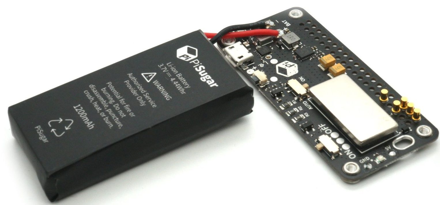
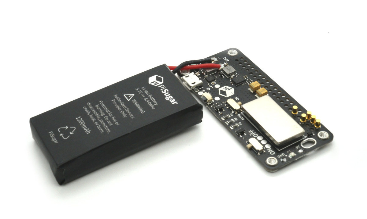
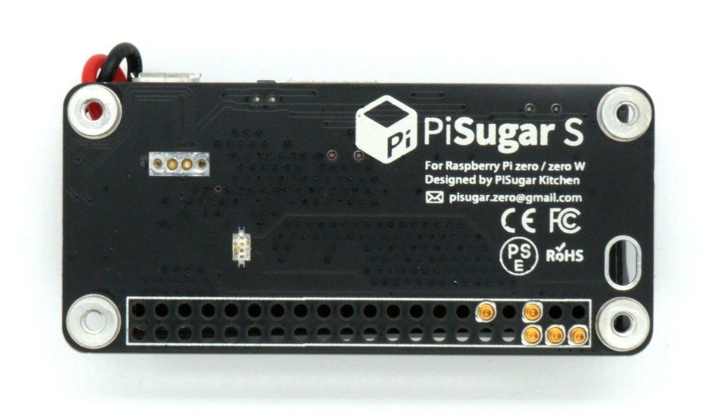
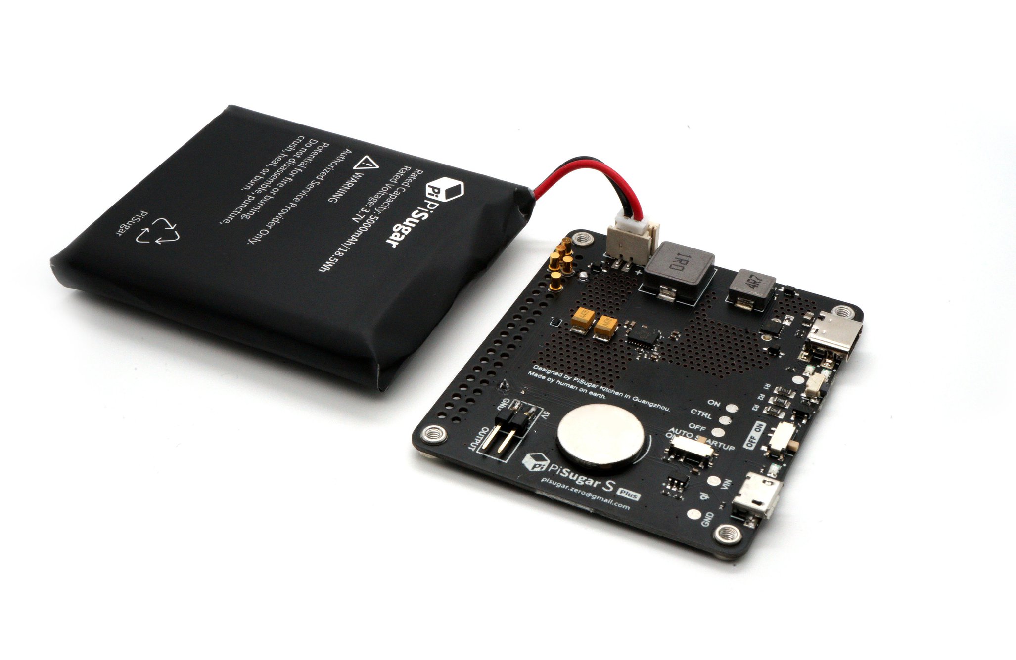
Powering the Raspberry Pi in battery-based applications is usually quite the hassle due to the high power consumption of the Pi and its sensitivity to voltage and current fluctuations. Guangzhou-based electronics manufacturer, PiSugar Kitchen, has over the past few years provided a variety of Battery Solutions for the Raspberry Pi but they have been at quite a steep price. To provide more options, and lower costs to the users, the company recently launched two new products; the PiSugar S and the PiSugar S Pro, designed to serve the different Raspberry Pi boards.
PiSugar S
Designed to serve the smaller boards like the Raspberry Pi Zero, Zero W, and Zero WH, the PiSugar S comes in a 65 x 30 x 1.5 mm form factor, just big enough to sit on the boards without taking up extra spaces on the sides of the Pi. It features a 1200mAh battery which is capable of reliably powering the Raspberry Pi Zero W for more than 6 hours, but users can get access to more juice with a 5000mAh battery option which can ensure the Pi stays powered for more than 10hours with 5V/2A supplied at the output.
Like previous Pi Sugar batteries, the PiSugar S works as an uninterruptible power supply (UPS) for the Raspberry Pi in that the device will continue to power the Pi without any interruptions when the external power supply is disconnected or connected. The system has the ability to detect the availability of the external power supply and switch input from the battery to the external power supply seamlessly. In situations where the device runs out of battery power, the provision of external power immediately turns on the device and can be used to trigger boot, which comes in handy for resetting remote devices.
The PiSugar S also comes with a configurable button that can be used to turn the device On (when OFF), or used as custom button input to your project, and an expansion through which solar and wireless charging can be added to the board.
The PiSugar S Pro, while retaining the UPS and other functionalities available on the PiSugar S, was designed to serve the bigger Raspberry Pi boards including the Pi 3B, 3B+, and the Pi 4B. Asides from matching the size of the bigger Raspberry Pi boards, the PiSugar S Pro also features a bigger battery (5000mAh) which is used to meet the 5v/3A requirements of the boards, with the ability to keep the boards on for more than 10 hours on battery power.
The PiSugar S is available for sale on the project’s Tindie page for $27.99 while the PiSugar S Pro goes for $29.99, without shipping.
More information on the PiSugar S and the PiSugar S pro can be found on the PiSugar Kitchen’s Page on Tindie and wiki.
We know from the Digital Logic Gates Introduction that a digital circuit at its input and output can have only two – states i.e. either “HIGH” or “LOW”. The logic “HIGH” and “LOW” are also termed as “1” and “0” logic, respectively. The voltage level at the input or output is the determinant of the logic “HIGH” or “LOW” and is dependent on the logic family. The Transistor-Transistor Logic (TTL) devices treat 2 to 5 Volts as logic “HIGH” and 0 to 0.8 Volts as logic “LOW”. Whereas, the Complimentary Metal-Oxide-Silicon (CMOS) devices use 3 to 18 Volts as logic “HIGH” and 0.15 Volts as logic “LOW”. The digital logic circuits are commercially available in form of an integrated circuit (IC)/ Chip and may have up to four logic gates inside.
The AND logic returns logic “HIGH” when all of its inputs are in the “HIGH” logic state. In other words, the output of AND gate will be “LOW” when any of the inputs is in the “LOW” logic state. In order to obtain a logic “HIGH”, all of its inputs should be “HIGH” and any of the input turning “LOW” will result in the output being driven to logic “LOW”.
Alternatively, the multiplication of “0”s and “1”s of the inputs gives the output state of AND logic. This gives the Boolean or logic expression of AND logic and is called Logical Multiplication. It is denoted by a dot (.) between the inputs of AND logic gate. For the inputs A and B, the Boolean expression is:
Q = A.B
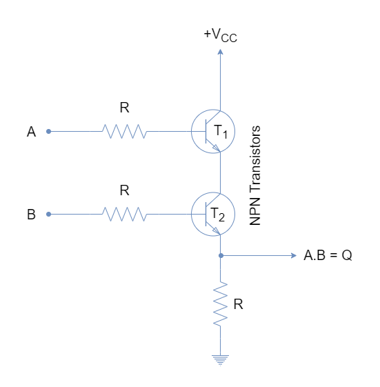
Resistor-Transistor AND Gate
In the following figure, a basic two-input AND gate constructed using Resistor-Transistor Logic (RTL) are shown. For each input, a Transistor (T) is used and the output is driven across the Resistor (R). In this type of AND logic circuit, the transistors are operated in saturated “ON” & “OFF” states.
Figure 1: The Resistor-Transistor Logic AND Gate
When both inputs “A” and “B” are “HIGH” then both transistors are in saturated “ON” states and a state “HIGH” appears at the output (Q). Turning any of the inputs to logic “LOW” will drive the relative transistor to the “OFF” state and thus incomplete path across VCC & Ground yields state “LOW” at the output (Q).
Logic AND Gate Symbol & Truth Tables
The representation of a AND logic by a symbol is shown in the following figure. Its symbol denotes the multiplication/ AND logic operation.
Figure 2: Logic AND Gate Symbol
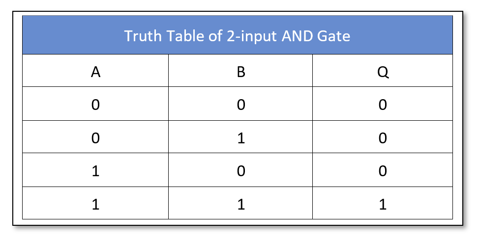
The truth table of a two-input AND logic gate is shown below:
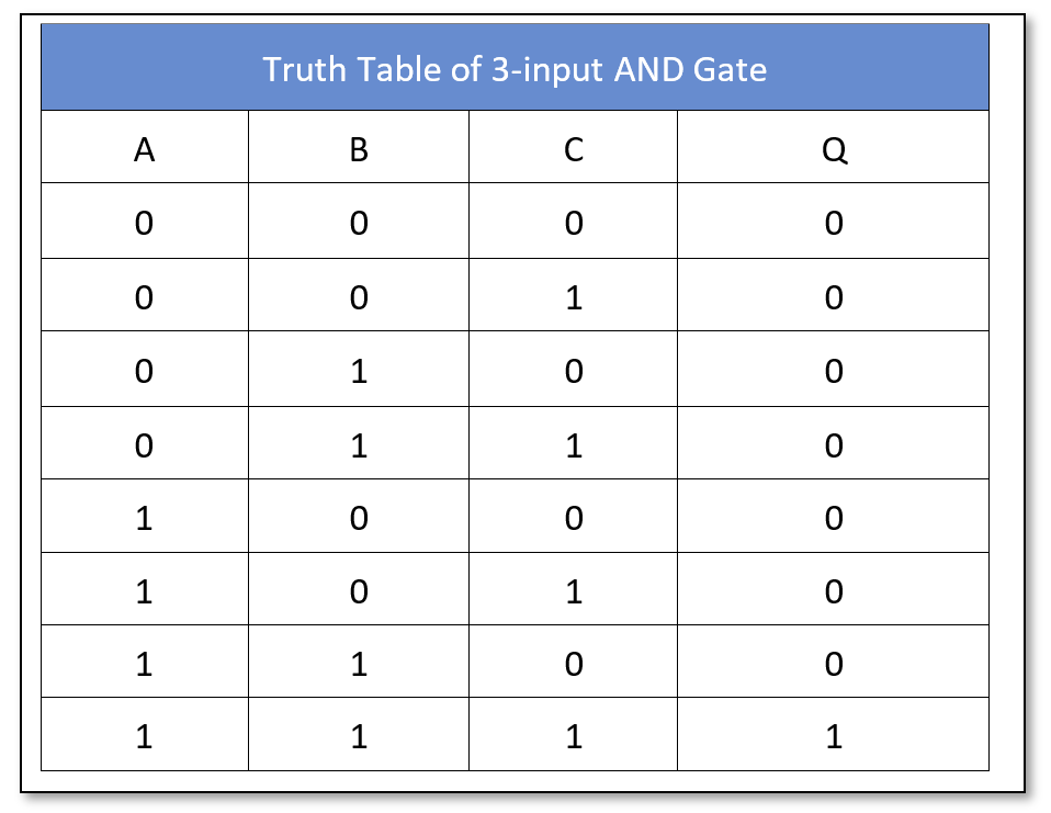
Similarly, the truth table of a three-input AND logic gate is as follow:
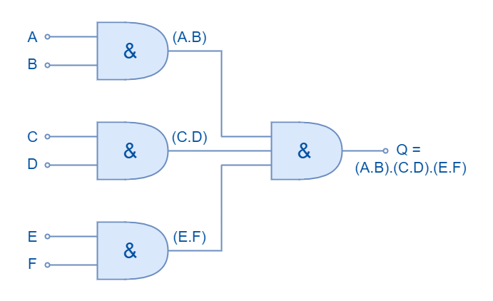
The Boolean expression can be extended to include multiple inputs to obtain AND logic operation. However, commercially available AND logic circuits have up to four inputs but the number of inputs can be further extended by cascading the AND logic circuits. In the following figure, three two-inputs gates and one three-input AND logic gate are cascaded to construct a six-inputs (2 x 3 = 6) AND logic circuit.
Figure 3: A 6-input AND logic constructed by cascading multiple AND gates
The Boolean expression for this cascaded circuit can be written as:
Q = (A.B).(C.D).(E.F)
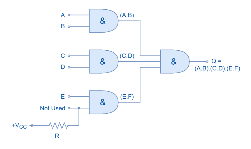
Odd Number of Inputs
The AND logic circuit having an odd number of inputs can be constructed by driving the unused input to logic “HIGH”. This will ensure that another input(s) of the AND logic gate is truly reflected at the output. It is explained in the following diagram where unused input is pulled high using a pull-up resistor.
Figure 4: The AND logic having an odd number of inputs
Commercially Available AND Gates
The AND logic gates are available in both TTL and CMOS logic families. The most commonly used AND logic packages are:
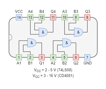
CMOS based AND Gate IC Package
CD4081 Quad 2-input
CD4073 Triple 3-input
CD4082 Dual 4-inputs
TTL based AND Gate IC Package
74LS08 Quad 2-input
74LS11 Triple 3-input
74LS21 Dual 4-input
Figure 5: 74LS08 & CD4081 Package having 2-input quad AND gates
Example of AND Logic
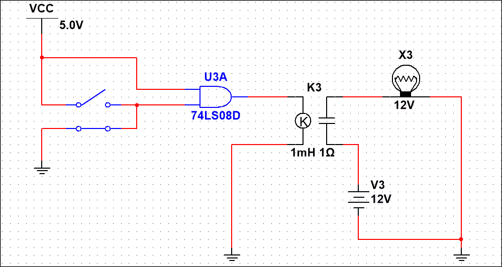
In the following figure, a AND gate is used to drive a 12V relay to switch on the lamp using NI Multisim. The AND gate (74LS08) energizes the relay when all of the inputs are connected to VCC. The relay thus turns on the lamp through an external circuit of 12V. When one of the inputs is connected to ground AND logic goes “OFF” turning the relay and lamp to “OFF” state as well.
Conclusion
The output of the AND logic is “HIGH” when all of the inputs are in logic “HIGH” states.
Any of the inputs in the logic “LOW” state will drive AND logic to the “OFF” state.
The AND logic gates can be constructed using Resistor-Transistor Logic (RTL) but are seldom used because of the propagation delay and power consumption.
The Transistor-Transistor Logic (TTL) and Complementary Metal-Oxide Semiconductor (CMOS) are commonly used.
The TTL uses a 5V supply whereas CMOS uses a 3-18V supply.
The AND logic gates commercially available have up to four AND logic inputs. However, inputs can be extended by using cascaded AND logic gates.
The AND logic circuit having an odd number of inputs can be constructed by using a pull-up resistor on the unused pin.
An external circuit can be controlled by AND logic with the use of a magnetic relay.
A couple of months back, AWS launched AWS IoT EduKit, which is an easy way to learn how to build IoT applications using AWS services. AWS IoT EduKit is developed in such a way that everyone from beginner to expert can build end-to-end IoT applications. For this, Amazon has partnered with M5Stack to provide a reference hardware kit.
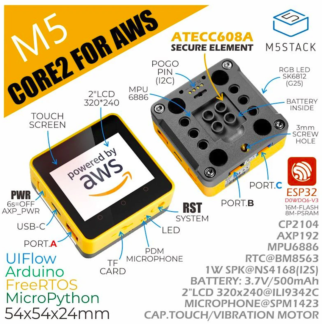
M5Stack Core2 for AWS is a reference hardware kit that comes with touch screen control and is widely used in IoT sensors, including temperature, accelerometer, gyroscope, and microphone.
The Core2 for AWS is a feature-rich, plug and play extensible, and secure hardware kit for learning and building a wide range of IoT applications. It comes equipped with a Microchip ATECC608A Trust GO secure element, in addition to the existing features of the standard M5Stack Core2 and M5GO Bottom2.
The Core2 IoT development kit has an ESP32-D0WDQ6-V3 microcontroller at its heart that comes with dual Xtensa 32-bit LX6 cores running at a frequency of 240Mhz. The microcontroller also supports wireless communication including 2.4GHz Wi-Fi, Bluetooth v4.2 BR/EDR, and BLE. The kit is manufactured with 16MB flash onboard which can be more than enough for small IoT applications.
Features:
CPU: ESP32-D0WDQ6-V3, dual Xtensa 32-bit LX6 cores and the main frequency of up to 240Mhz
Memory: 8M PSRAM
Storage: 16M flash storage, TF card slot (support up to 16GB)
Wireless connectivity: 2.4GHz WiFi, Bluetooth 4.2, BLE
Edukit is Alexa capable of coming up with multiple onboard peripherals and expansion modules for connectivity options like LoRaWAN, NB-IoT, and LTE. Also, come with plug play grove-connector peripherals for the user to connect sensors and actuators. With the support of LoRaWAN, the kit is expected to gain traction for a variety of IoT applications majorly in agriculture.
The hardware supports several application frameworks like FreeRTOS, Arduino, and MicroPython that will allow the users to program in the language and design embedded applications on a single hardware platform. Also, with the collaboration of AWS and M5Stack, you can now use Espressif’s RainMaker platform and PlatformIO development platform. With the RainMaker platform, you can now control the smart home application without an AWS account, while with PlatformIO development platforms can be used to edit and flash code on the hardware.
The main unit also has a 2.0-inch capacitive touch screen that enhances the user experience on smart homes and small agriculture applications. More hardware specifications are available on the M5Stack Docs. If you plan to buy and play with the development kit, head to the product page on the M5Stack product page where it is priced at $49.90 plus shipping.
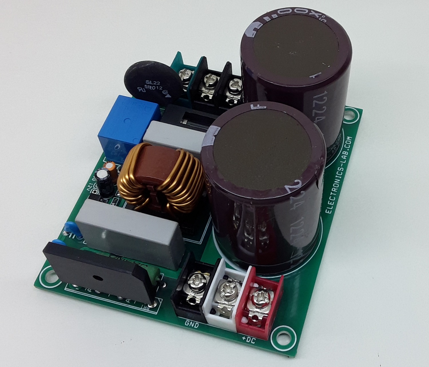
Although this power supply design is specific to the Intelligent Power Modules (IPM), the concepts and circuit design may be used for any power supply that requires high voltage output up to 400V DC and 6 A. It is an unregulated power supply, DC output is dependent on AC input. The circuitry includes a passive EMI filter consisting of elements C5, C6, C7, C8, C9, C10, T1, and a BR1 25 A/600V rectifier block, R3 NTC for inrush current protection, and a relay RL1 for soft powering up and reducing conduction losses in steady-state operation. 2 x electrolytic capacitors C3, C4 are used for buffering the rectified DC bus voltage. It is advisable to use a heatsink on the bridge rectifier. Inrush current circuit requires 12-15V DC @ 50mA power supply. Choose appropriate fuse as per current requirement.
High Voltage DC Power Supply for Intelligent Power Modules – [Link]
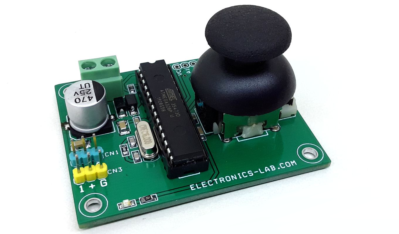
This project enables easy control of 2 RC servo motors using a thumb joystick. This is an Arduino compatible project and it consists of a thumb joystick, ATMEGA328 microcontroller, filter capacitor on dc supply, and other components. The thumb joystick has 2 axes, X and Y. The joystick consists of 2 x 10K potentiometers. These potentiometers provide analog voltage output as per the movement of each axis. The microcontroller reads this analog voltage and converts it to RC PWM pulse. The PWM frequency is 50Hz and the duty cycle is 1ms to 2ms. Connect the RC servos to connector CN1 and CN3, apply 5V power supply to connector CN2 and you are ready to go. I have used a high-value electrolytic capacitor on DC supply for the smooth operation of RC Servo. It is important to use at least 1-3A power supply or batteries for the proper smooth operation of the servos and to avoid vibrations. It can be used to control small camera pan-tilt head, robotics, robotics arm, animatronics, toys etc.