DFRobot DFR0756 DC-DC Fast Charge Module

DFRobot DFR0756 DC-DC Fast Charge Module integrates the most common 5V charging-recognition function and provides compatibility for more than 99% of mobile phones on the market. The charging current at the peak of this module can be triggered by the charging protocol, which greatly saves charging time. This fast-charging module is capable of providing steady output and thereby works for a long time without voltage shift. Typical applications include projects like mobile phone fast charging, car charging retrofit, solar charger, and DIY power sources.

Features

  • Compact size
  • 5V charging recognition function
  • Support multiple fast-charging protocols
  • USB output
  • Can be used as a charging module or power supply

Specifications

  • Output voltage:
    • 3V to 12V auto-adjust based on the fast-charging protocol
    • Default output 5V, the input should be 2V higher than the output
  • 0-3A output current
  • Supported Fast Charging Protocol:
    • DCP protocol, BC1.2, Apple, Samsung
    • Huawei fast charging protocol FCP/SCP
    • Supports Spreadtrum Fast Charge Protocol (SFCP)
    • Qualcomm QC 2.0 and 3.0
    • MTKPE1.1/PE2.0
  • 6V to 32V input voltage range
  • Chip protections:
    • Input overvoltage
    • Under-voltage protection
    • Input overcurrent protection
    • Output overcurrent protection
    • Short circuit protection
    • Machine over-temperature protection

more information: https://www.dfrobot.com/product-2163.html

u-blox’s SARA-R5 LTE-M/NB-IoT Modules are secure cloud LTE solutions

u-blox’s modules offer security-based features and services like zero-touch provisioning and secure chip-to-chip communication

u-blox’s SARA-R5 series modules are secure cloud LTE Cat M1/LTE Cat NB2 solutions based on the UBX-R5 cellular chipset and the M8 GNSS receiver chip. With this combination, u-blox can offer long-term device availability and provide lifetime support of the entire platform, down to the chipset level. The SARA-R5 series also offers security-based features and services like local data protection, zero-touch provisioning, anti-cloning, and secure chip-to-chip communication.

The LTE-M and NB-IoT modules support a comprehensive set of 3GPP Rel. 14 features that are relevant for IoT applications, like improvements to power consumption, coverage, data rate, mobility, and positioning. They are 5G-ready, meaning customers will be able to upgrade the software of their deployed devices once 5G LTE has been rolled out by mobile operators, greatly improving product scalability and lifetime.

The SARA-R5 series includes three secure Cloud variants that support u-blox IoT-Security-as-a-Service, making these the ideal choice for devices that transmit critical and confidential information. The SARA-R500S secure Cloud module is the cost-effective solution, the SARA-R510S secure Cloud module is optimized for extremely low power consumption in deep-sleep PSM, and the SARA-R510M8S secure Cloud module has an integrated u-blox M8 GNSS receiver chip and a separate GNSS antenna interface. In addition, the SARA-R510M8S module offers unique hybrid positioning, in which the GNSS position is enhanced with u-blox CellLocate® data, providing location always and everywhere.

SARA-R5 series modules are form-factor compatible with the u-blox LISA, LARA and TOBY cellular module families and they are pin-to-pin compatible with the u-blox SARA-R4, SARA-N2, SARA-N3, SARA-N4, SARA-G3, SARA-G4, and SARA-U2 cellular modules families.

Features

  • Built-in secure cloud functionality with hardware-based root-of-trust inside a discrete secure element
  • IoT security-as-a-service with foundation, design, end-to-end security, and access control
  • Optimized ultra-low power consumption: less than 1 µA of current in power saving mode (PSM)
  • Data communications up to 1,200 kbits/s
  • Extended operating temperature range: -40°C to +85°C
  • Critical firmware updates delivered and services enabled via uFOTA
  • Accurate and reliable positioning with u-blox M8 GNSS receiver (SARA-R510M8S)
  • -00B version: LTE-M only for US and EU + global roaming
    • Security-based features:
      • Key management system
      • Zero-touch provisioning
      • Local data protection
      • Local chip-to-chip security
      • Local data protection
  • -01B version:
    • -00B features plus:
      • NB-IoT for EU, Taiwan, and Australia
      • E2E data integrity
  • Thingstream anywhere

more information: https://www.u-blox.com/en/product/sara-r5-series

ICP-10111 Barometric Pressure Sensor consumes only 1.3 µA @ 1Hz

TDK Invensense’s ICP-10111 is ideal for mobile phones, wearable fitness monitoring, drones, and battery-powered IoT

TDK Invensense’s ICP-10111 barometric pressure sensor is based on MEMS capacitive technology, which provides ultra-low noise at the lowest power, enabling excellent relative accuracy, sensor throughput, and temperature stability. The pressure sensor can measure pressure differences with an accuracy of ±1 Pa, an accuracy enabling altitude measurement differentials as small as 5 cm, less than the height of a single stair step.

Consuming only 1.3 µA at 1 Hz, available in a small footprint 2.0 mm × 2.5 mm × 0.92 mm 8-pin LGA package, the ICP-10111 is ideally suited for mobile phones, wearable fitness monitoring, drones, and battery-powered IoT.

The ICP-10111 offers a temperature coefficient offset of ±0.5 Pa/°C. The combination of high accuracy, low power, and temperature stability in a small footprint enables higher performance barometric pressure sensing for sports activity identification, mobile indoor/outdoor navigation, and altitude-hold in drones.

Features

  • Pressure operating range: 30 kPa to 110 kPa
  • Noise and current consumption:
    • 0.4 Pa at 10.4 µA (ULN mode)
    • 0.8 Pa at 5.2 µA (LN mode)
    • 3.2 Pa at 1.3 µA (LP mode)
  • Pressure sensor relative accuracy: ±1 Pa for any 10 hPa change over 950 hPa to 1050 hPa at +25°C
  • Pressure sensor absolute accuracy: ±1 hPa over 950 hPa to 1050 hPa, 0°C to +65°C
  • Pressure sensor temperature coefficient offset: ±0.5 Pa/°C over +25°C to +45°C at 100 kPa
  • Temperature sensor absolute accuracy: ±0.4°C
  • Temperature operating range: -40°C to +85°C
  • Host interface: I2C at up to 400 kHz
  • Single supply voltage: 1.8 V ±5%
  • Small footprint of 2.0 mm × 2.5 mm × 0.92 mm
  • 8-pin LGA package
  • RoHS and green compliant

more information: https://invensense.tdk.com/products/1-axis/icp-101xx/icp-10111/

IRR1-SOL Solar Irradiance Meter helps troubleshooting of photovoltaic installations

Fluke’s IRR1-SOL solar irradiance meter is designed to simplify the installation and troubleshooting of photovoltaic arrays in a single handheld tool

Solar energy converts the sun’s energy into electricity; solar technology is improving with costs of going solar decreasing rapidly. Fluke’s IRR1-SOL solar irradiance meter provides industrial, residential and commercial installation and maintenance professionals with a single handheld tool designed to simplify the installation, commissioning, and troubleshooting of photovoltaic arrays, measuring irradiance, temperature, inclination, and direction of the solar array.

The simple user interface, instantaneous solar irradiation measurements, and built-in temperature sensor make it easy to meet the IEC62446-1 requirements for testing, documenting, and maintaining photovoltaic systems.

The meter can measure irradiance by simply placing the meter directly onto the PV panel. The integrated compass and inclination sensor also allows quick measurement and documentation of roof and site orientation, pitch, and panel tilt, while surveying, installing, or adjusting an installation.

  • Optimizes placement on solar power systems and verifies window efficiency
  • Measures solar output used to calculate overall energy efficiency and placement of solar systems

Features

  • Measure solar irradiance, ambient and PV module temperature, array orientation, and tilt angles
  • Make instantaneous measurements to determine the watts per square meter solar irradiation required by IEC 62446-1 standard
  • High contrast LCD with large numbers for easy readability in direct

more information: https://www.fluke.com/en-us/product/electrical-testing/best-solar-energy-industry-tools/flk-irr1-sol

LE-37O – 3.5 inch Miniboard Intel® Tiger Lake UP3 Processor

Taiwan Commate Computer Inc.(COMMELL), the worldwide leader of Industrial Single Board Computers, unveiled LE-37O 3.5 inch Miniboard embedded system board based on Intel® Tiger Lake UP3 processors.

The LE-37O 3.5 inch Miniboard platform is designed for Intel® Tiger Lake UP3-series processors in the FCBGA1449 sockets. support DDR4 memory (One DDR4 SO-DIMM 3200 MHz up to 32GB).

The platform is based on Intel® UHD Graphics, this GPU offers 24 execution units (EUs) clocked at up to 1150Mhz(depending on the CPU model), The revised video engine now decodes H.265/HEVC completely in hardware and thereby much more efficiently than before. Displays can be connected via1 VGA, 1 LVDS,1 HDMI and one DP port up to four displays can be controlled simultaneously. LE-37O offers lots of features including high-speed data transfer interfaces such as 4 x USB3.2 Gen2 and 2 x SATA3, equipped with dual Gigabit Ethernet, and comes with PS/2 port, 2 x RS232 and 2 x RS232/422/485, 2 x USB2.0, Intel® High Definition Audio, and 1 MiniPCIe socket(Supports mSATA), 1 M.2 (Key E 2230), 1 M.2 (Key M 2280) for NVMe.

Key Features:

  • CPU: Intel® Tiger Lake UP3 Processor in the FCBGA1449 sockets.
  • Memory: One DDR4 3200 MHz SO-DIMM up to 32 GB, support Non-ECC, unbuffered memory.
  • Integrated Graphics: Intel® Iris® Xe Graphics.
  • LVDS interface: Onboard 18/24-bit single/dual channel LVDS connector with +3.3V/+5V/+12V supply
  • Display port interface: Onboard Display port connector.
  • HDMI interface: Onboard HDMI connector.
  • VGA interface: Onboard VGA connector.
  • LAN Interface: 1 x Intel® i219-LM Gigabit PHY LAN(Support iAMT 15.0), 1 x Intel® i225-LM Gigabit LAN (up to 2.5GbE).
  • Serial ATA: Support 2 x SATA3.
  • Audio: Realtek ALC262 High Definition Audio.
  • Internal I/O: 2 x SATA3, 2 x RS232,  2 x RS232/422/485, 2 x USB2.0, 1 x LVDS, 1 x LCD inverter conector, 1 x GPIO, 1 x Audio, 1 x PS/2, 1 x SMBus.
  • Rear I/O: 1 x DisplayPort, 1 x HDMI, 1 x VGA, 4 x USB3.2 Gen2, 2 x LAN.
  • Extended interface: One PCIE Mini card (Support mSATA), one M.2 (Key E 2230) for Wi-Fi and Bluetooth, one M.2 (Key M 2280) for NVMe.
  • GPIO interface: Onboard programmable 8-bit Digital I/O interface.
  • Power requirement: DC input 9~35V.

more information: http://www.commell.com.tw/Product/SBC/LE-37O.HTM

Joystick Controlled 2 x RC Servo motors – Arduino Compatible

This project enables easy control of 2 RC servo motors using a thumb joystick. This is an Arduino compatible project and it consists of a thumb joystick, ATMEGA328 microcontroller, filter capacitor on dc supply, and other components. The thumb joystick has 2 axes, X and Y. The joystick consists of 2 x 10K potentiometers. These potentiometers provide analog voltage output as per the movement of each axis. The microcontroller reads this analog voltage and converts it to RC PWM pulse. The PWM frequency is 50Hz and the duty cycle is 1ms to 2ms.  Connect the RC servos to connector CN1 and CN3, apply 5V power supply to connector CN2 and you are ready to go. I have used a high-value electrolytic capacitor on DC supply for the smooth operation of RC Servo. It is important to use at least 1-3A power supply or batteries for the proper smooth operation of the servos and to avoid vibrations. It can be used to control small camera pan-tilt head, robotics, robotics arm, animatronics, toys etc.

Arduino Programming

Note: Project is Arduino compatible, Arduino code provided as a download. New ATMEGA328 requires bootloader and firmware uploading, refer to the link below to learn uploading the code into the chip.

Features

  • Supply 5V DC – 2A
  • 2 x RC Servo motors
  • Power LED
  • PCB dimensions: 61.12 x 47.63 mm

Schematic

Parts List

NO.QNTY.REF.DESC.MANUFACTURERSUPPLIERSUPPLIER PART NO
12CN1,CN33 PIN MALE HEADER PITCH 2.54MMWURTHDIGIKEY732-5316-ND
21CN22 PIN SCREW TERMINALPHOENIX CONNECTDIGIKEY277-1247-ND
32CN4,CN5DNPOMIT
42C1,C222PF/50V SMD SIZE 0805MURATA/YAGEODIGIKEY
53C3,C4,C60.1uF/50V SMD SIZE 0805MURATA/YAGEODIGIKEY
62C5,C810uF/16V SMD SIZE 1206MURATA/YAGEODIGIKEY
71C7470uF/25V ELECTROLYTICPANASONICDIGIKEYPCE4886TR-ND
81D1LED RED SMD SIZE 0805DIGIKEY
92D2,D31N4007DIODE INCORP.DIGIKEYS1MBDITR-ND
101R11M 5% SMD SIZE 0805MURATA/YAGEODIGIKEY
112R2,R3JoystickC&kDIGIKEY108-THB001P-ND
121R410K 5% SMD SIZE 0805MURATA/YAGEODIGIKEY
131R51K 5% SMD SIZE 0805MURATA/YAGEODIGIKEY
141U1ATMEGA328DIPMICROCHIPDIGIKEYATMEGA328-PU-ND
151Y116MHZECS INCDIGIKEY X1103-ND

Connections

Gerber View

Photos

Video

THB001P Datasheet

Humidity Meter Using OLED Display – Arduino Compatible

This is an easy to build, very compact, and low profile Arduino compatible platform to build a humidity meter/Gauge using a 0.96Inch OLED display. The project consists of Atmega328 microcontroller, 0.96Inch OLED display, 3.3V regulator, and HIH5030 analog humidity sensor from Honeywell. The HIH5030 sensor provides an analog voltage output, the analog voltage is near linear voltage output vs %RH, the sensor output is connected to A0 (Arduino-ADC pin 0) of the ATmega328 microcontroller. The sensor output is 0.25V to 2.5V vs 0 to 100% RH. Connector CN2 is provided for boot-loader flashing and Arduino programming. Use Pin 4 GND and Pin5 VCC to power the project.

Humidity Meter Using OLED Display – Arduino Compatible – [Link]

Meet AIfES, a C-based AI/ML Framework for Microcontrollers

Increased interest in Edge computing in recent times has led to the development of several frameworks to facilitate the deployment of AI/ML models on microcontrollers. There are, however, issues of performance with most of the frameworks as they are mostly scaled-down version of server codes and as such, are only suitable for fairly powerful microcontrollers.  To solve this and provide a framework to support even the lowest of 8-bit MCUs, the Fraunhofer Institute for Microelectronic Circuits and Systems (IMS) recently announced the release of the AIfES (Artificial Intelligence for Embedded Systems); an open-source framework to facilitate the deployment of AI on all forms of microcontrollers.

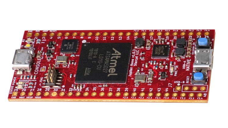
Developed using the C programming language, AIfES allows users to quickly, and quite easily, train and run artificial neural networks (ANN) on almost any hardware, including 8-bit MCUs and development boards based on them like the Arduino Uno, without the need to prepare the models on a PC. ‘While featuring significantly reduced functionalities due to the desire to target Low processing power MCUs, AIfES is comparable and compatible with most of the popular ML frameworks like TensorFlow, Keras, and PyTorch, incorporating most of their popular features.

It currently supports feedforward neural networks (FNN),  along with common activation functions like ReLU, sigmoid, and softmax, and common training algorithms like gradient descent optimizer (SGD) or the adam optimizer, all integrated with a full implementation of Convolutional Neural Networks (ConvNet) also on the way. The model development is based on the Python frameworks, and ANN Models developed on those frameworks can also be easily imported into the AIfES framework. All of this makes the transition to AIfES seamless for users that are already familiar with other popular AI frameworks.

One of the many other good things about AIfES is how it allows developers to allocate resources, like specifying the required memory area for an ANN. It is also modular in such a way that different components of algorithms can be exchanged, which makes it easy to use different types of hardware accelerators, and finding one that is compatible with your embedded device easy.

According to the folks at the Fraunhofer IMS, in-house researchers have been using AIfES in AI research and development for years, and it featured in several Custom solutions until a level of development was reached where it could be used as a stand-alone product.

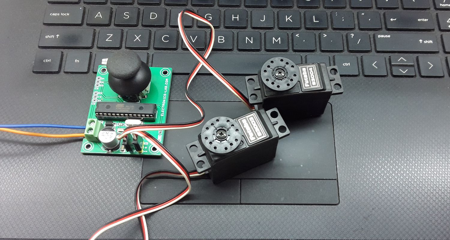
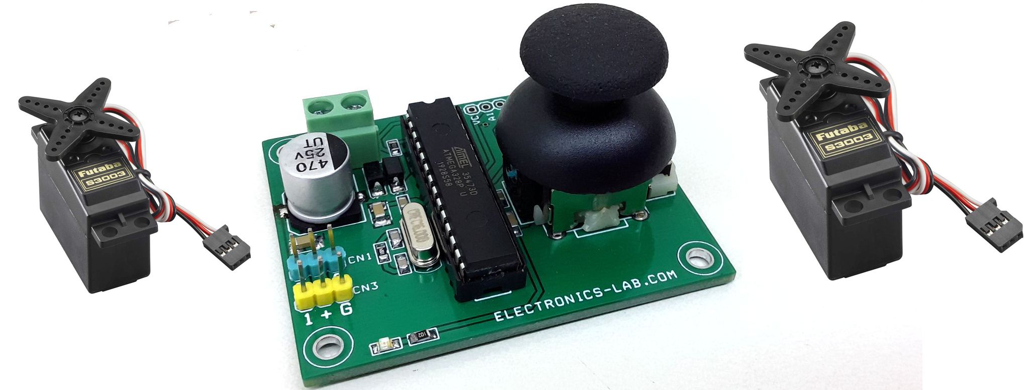
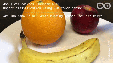
During this period, AIfES featured in several applications including a wireless current sensor for condition monitoring, a gesture recognition system, and an Arduino Uno based handwriting recognition system which is a perfect showcase for the prowess of the framework on 8-bit microcontrollers.

The compatibility of AIfES for microcontrollers was further expanded with the recent release of its Arduino Library, which means makers familiar with the Arduino environment can easily build AI solutions based on Arduino and derivative boards.

The library can be easily installed via the Arduino Library Manager. AIfES is offered as a dual license model. For private projects or developers of free open-source software under the GNU General Public License (GPL) version 3, AIfES can be used free of charge. However, for users seeking to use AIfES in commercially licensed software, a commercial license agreement must be obtained from the Fraunhofer IMS.

More information on the project, its capabilities, examples, and license descriptions is available on the project’s GitHub page.

Rodriguez – The World’s Slowest IV Tracer

Joseph Eoff has posted on Hackaday details about Rodriguez, which is an IV tracer. About the origin of the project, he says:

“Rodriguez started as a nameless project I used to make a point in an online discussion about the shape of the current/voltage plot of the base/emitter junction of an NPN transistor. It’s as a simple one-off for a specific purpose, and sort of mushroomed. From a simple circuit and software to plot the current and voltage curve of a single diode junction, it has grown into a functional (if limited) current and voltage tracer that can be used to design small transistor amplifiers.”

He started by plotting Vbias against the base current. This is the result:

After successfully plotting Vbias, He realized that he had solved all of the problems involved in making a current/voltage tracer for transistors. He made use of Current/voltage traces to design the transistor amplifiers using the load line method of design. This is what current/voltage plot of a typical transistor looks like:


The circuit he built for Rodriguez featured a few passive components and an Arduino. Arduinos have some low-resolution analog to digital converters and PWM outputs that can be used to generate analog voltages and currents. Rodriguez employs a couple of tricks to derive usable results out of its very crude hardware. For its good resolution on the signals generated by the PWM outputs, it utilizes the Timer1 library.  The Timer1 library enables free choice of the PWM frequency and 10 bits of resolution for the pulse width (that’s 1024 steps.)  With a PWM frequency of 10kHz, Rodriguez is able to operate with a very simple low pass filter to make the analog signals. Also, with 1024 steps, the plots are smoother than they would be with just 256 steps.

Rodriguez utilizes oversampling to derive the equivalent of 14 bits of resolution out of the 10 bit ADCs.  For accurate measurements of the base current, it goes further and oversamples the oversampling which it oversamples by 256 for most measurements.  The base current measurements are oversampled 256 times the regular oversampling. The oversampling method gives Rodriguez enough resolution to be useful but however, makes the program very slow.

Rodriguez boasts of the simplicity of its circuit. You only need two capacitors, 5 resistors, and an Arduino of any flavor. It is easy to assemble. About the assembly of Rodriguez, he says

“I built mine as a sort of 3D sculpture on the pin header of the Nano.  It could just as easily be assembled on a solderless breadboard.  Perfboard would work as well.  An etched PCB would be rather overkill, but whatever floats your boat.”

You can find the software on github repository, which also includes a schematic of the required circuit and the Arduino program.

For now, Rodriguez can make current/voltage plots of bipolar junction transistors and diodes, which he tested on 2N3904, 2N3906, and 2N2222 transistors.  He also used it on LEDs of various colors, as well as regular diodes (1N4148, 1N4001.) for future upgrades, he says

“I plan to add support for FETs in the future, but I have to order some for experiments. I will also add a save/load feature for the collected data.”

Rodriguez is quite limited in the current and voltage it can deliver to the device under test.  You can’t get more than 5 volts or about 5 milliamperes out of it.  That’s enough for testing small signal diodes and small transistors.  You won’t be designing a class A power amplifier with Rodriguez, but it will do for learning the principles of amplifier design using the load line method.

For more information, visit the project page on Hackaday.

Meet the Jupiter Nano, The Tiny, high-performance computer that runs Linux, and the NuttX RTOS

Over the past year since its launch, we’ve seen several interesting projects come out of the Microchip Get Launched program. The latest, which according to Crowd supply, will be hitting the crowdfunding campaign site soon, is the Jupiter Nano.

A tiny, Open-Source, high-performance development board, capable of running a Linux based OS or the NuttX real-time OS, the Jupiter Nano features the Microchip SAMA5D27C-LD1G Cortex A5 processor packed into a 1.125″ x 2.5″ teensy-like form factor with 48 GPIO pins.

Coming with 10x the power of the Arduino due, the Jupiter Nano was designed to be a perfect replacement for Arduino users who need a tiny, powerful computer with more CPU power, lots of RAM, and the ability to deploy an internet-connected real-time operating system like the NuttX.

To expand its offerings and open doors to Linux-based users, the board also supports Linux-based operating systems, with lots of I/O and high-speed Wi-Fi.

Some of the highlight features and specifications of the new board as listed on its crowd supply page includes:

  • Microchip SAMA5D27C-LD1G Cortex A5 Processor running at 498 Mhz
  • AP Memory AD2100XXX 128 M x 32 LPDDR2 DRAM chip integrated into system-in-package (SIP)
  • NuttX RTOS or Linux
  • Tiny 48-pin form factor (1.125″ x 2.5″, similar in size to Teensy 4.1)
  • Key peripherals use DMA (USB, SPI, I2C, Flexcom)
  • JTAG port for programming and debugging
  • USB 2.0 HS port on USB-micro B jack (Port A, 480 Mbps, host or device)
  • USB 2.0 HS port on a pin-header connection (Port B, 480 Mbps, host only)
  • USB 2.0 FS Debug console port on USB-micro B jack (12 Mbps)
  • SD Card slot – 50 MHz DDR – device boots from the card (this means it is impossible to brick the device)
  • Native SPI and I2C ports
  • 4 FLEXCOMs on I/O pins – flexible serial controller peripherals that can be SPI, UART, or I2C
  • Qorvo ACT8945A with integrated LiPo battery charging capability
  • Compatible with many LiPo Batteries
  • Open Source Hardware with all design files (KiCAD) available.

According to the project page, the board is totally open source and all files, including PCB Design files, schematics, and software will be made available on Github once the project achieves its funding goals.

There is no price information yet, but this definitely will be available as soon as the crowdfunding campaign begins.

To learn more about the project, the features of the board, and signup to be notified when the campaign begins, you can visit the project’s page on CrowdSupply.

TOP PCB Companies