BastWAN RAK4260 Module Based Dev-Board in Feather Form Factor

BastWAN RAK4260 Module Development Board

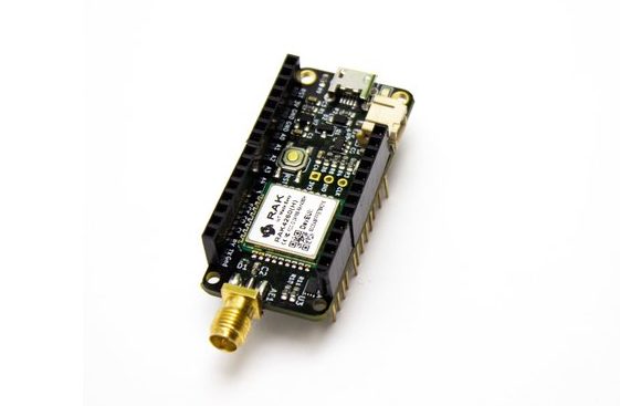
With the increasing popularity of the Adafruit Feather form factor in recent years, many third-party manufacturers have developed Feather-compatible boards, such as the Penguino Feather 4260, Giant board, OrangeCrab, and Feather-S2. Mexico-based Electronic Cats has come up with their own Feather-compatible board with LoRa connectivity: BastWAN.

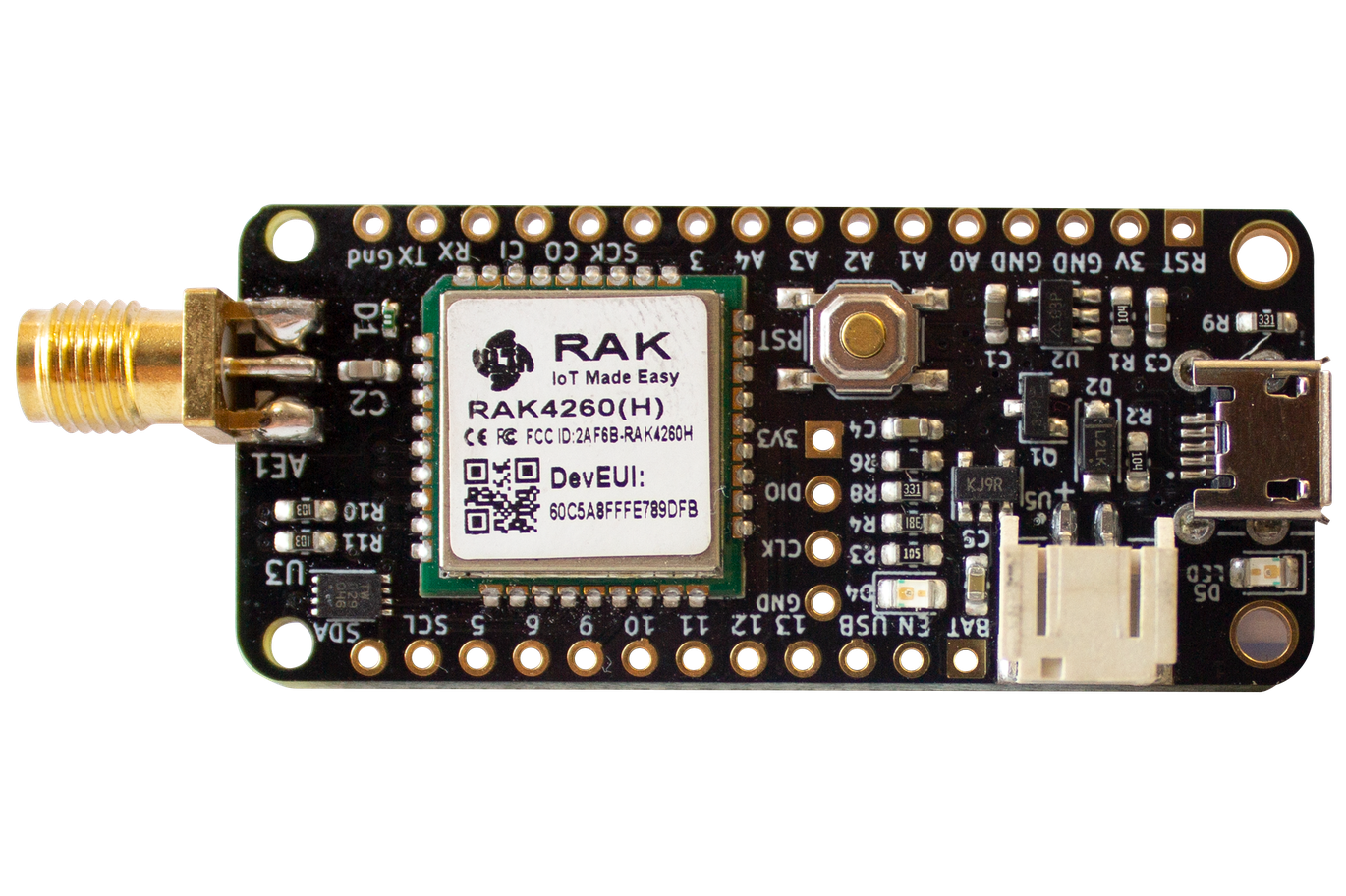
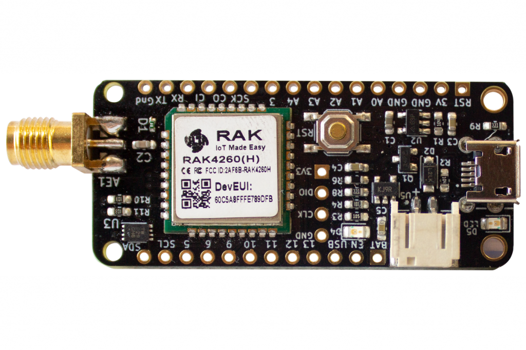
A high-performance, ultra-low-power RAK4260 module based on Microchip R34 LoRa® System-in-Package (SiP) powers the development board. Additionally, the UF2 USB bootloader comes pre-installed on BastWAN, and it’s completely assembled, tested, and programmed.

BastWAN is perfect for beginners and advanced developers, and it is similar to the Penguino Feather 4260. But unlike the Penguino board, BastWAN uses only an SMA antenna connector (no uFL option). But lacks an RGB LED and substitutes the USB-C port with a Micro USB port for power and debugging. Additionally, BastWAN provides SWD support through four holes rather than a 10-pin connector.

Discussing further, Microchip R34 is an industry’s ultra-low-power LoRa (Long Range) SiP device which includes an integrated 48Mhz SAML21 32-bit microcontroller and a LoRa transceiver. It operates in the range of 862 to 1020 MHz frequency. It is designed for ultra-long range spread spectrum communication-based applications with minimal line-power demand.

BastWAN RAK4260 Module Front

Features of BastWAN Feather-compatible Board

  • RAKWireless RAK4260 module based on low-power Microchip R34 LoRa SiP device with SAM L21 Arm
  • Cortex M0+ MCU and LoRa transceiver for connectivity.
  • It has up to 32 KB RAM and 256 KB of Flash
  • Rapid prototype with LoRa/LoRaWAN technology
  • 20 IO pins available on pin headers— PWM, Serial, I2C, SPI, 6x 12-bit ADC, 1x 10-bit DAC.
  • The ATECC608A crypto authentication chip ensures secure communication.
  • There are three power supplies available. These include 5V via a micro USB port, a 2-pin header for a LiPo battery, and a 3.3V regulator with a peak current of 500mA.
  • The board also includes a built-in 100mA LiPo charger with a charging status indicator, an SMA antenna connector, a micro-USB port, a reset pin, and a button.
  • For easy software development, the Arduino environment is fully supported including a LoRa compatible software stack.
  • Dimensions – 50.8 mm x 22.8 mm
  • Weight 6.9 grams

The Feather-format board also includes a Microchip ATECC608A cryptographic coprocessor which provides hardware-based security and hardware-based key storage, both of which are useful for connecting your projects to the cloud. It features a built-in USB, thus it provides a USB-to-Serial program and debugs functionality “with no need for an FTDI-like chip”.

Coming to the software part, the BastWAN comes pre-loaded with the UF2 bootloader. It appears as a virtual disk drive, so reprogramming is as easy as dragging and dropping the firmware file. Additionally, as the bootloader is BOSSA compatible, it can be used directly within the Arduino integrated development environment (IDE), MakeCode, and other programming environments.

BastWAN is available for $31.39 on Tindie. For more information visit the product page. Images and technical specifications have also been taken from the product page.

Melexis MLX90392 Triaxis Micropower Magnetometer

Melexis MLX90392 Triaxis® Micropower Magnetometer is a programmable sensor IC offering a 16-bit output proportional to the magnetic flux density sensed along the XYZ axes, along with temperature output signal. The MLX90392 is based on Melexis proprietary Triaxis technology. By selecting which axes are to be measured, the raw data can be used as input for further post-processing by an external microcontroller, making the device suitable for applications such as joysticks, rotary knobs, linear strokes, and complex 3D position sensing.

The MLX90392 is available in 2 magnetic variants:

  • ±5mT range for low noise applications (MLX90392ELQ-AAA-010-xx)
  • ±50mT range for for position sensor applications (MLX90392ELQ-AAA-011-xx)

The Melexis MLX90392 Triaxis Position Sensor is offered in a compact 2.0mm x 2.5mm UTDFN-8 package, ideal for space-constrained applications.

Features

  • Programmable parameters on the fly
  • 0mT to 5mT/5mT to 50mT magnetic range
  • Triaxis Hall technology
    • 1µTrms  for the ±5mT variant
    • 7µTrms  for the ±50mT variant
  • Micropower
    • Power down current of 1.5µA
    • Supply voltage of 1.8V
  • Selectable modes
    • Single Measurement
    • Continuous Mode up to 1.4kHz (XYZ)
  • Fields of motion
    • On-axis
    • Off-axis
    • Joystick
    • Linear
  • Integrated temperature sensor
  • Digital 16-bit output for magnetic and temperature (XYZT)
  • I2C output interface; 1.4kHz data rate
  • Operating temperature range from -40C to +85℃
  • 2.0mm x 2.5mm x 0.4mm UTDFN-8 package (JEDEC qualified)

more information: https://www.melexis.com/en/product/mlx90392/3d-magnetometer-micro-power-and-cost-conscious

Fibocom Meets MWC21: Unleash the Value of IIoT with the Intersection of 5G, AI and Edge Computing

Mobile World Congress Barcelona, the world’s largest mobile ecosystem event, returned as hybrid event this year, providing the world an opportunity to explore ground-breaking innovations and the latest trend in the mobile world. Fibocom, a global leading provider of IoT (Internet of Things) solutions and wireless communication modules, focuses on the best practices in 5G verticals for industry users.

Fibocom Insights

Among all the topics being discussed this year, combining 5G connectivity with Artificial Intelligence (AI) and edge computing to develop Industrial IoT (IIoT) solutions has attracted much attention. Industry users have been actively investing in IIoT for operational efficiency, which is helpful for real-time decision-making to minimize waste and prevent equipment failure. IIoT applications, meanwhile, generated more data than ever before. Businesses and industry experts are turning to the Artificial Intelligence of Things (AIoT), the convergence of AI and IoT, to make smarter decisions more quickly.

Since massive amounts of data have been collected and most of them are unused, the inability for humans to analyze all of the data produced is why businesses seek to incorporate AI and edge computing into Industry 4.0. On the one hand, with the help of AI, AIoT systems can proactively detect failures and events, enabling predictive maintenance. Edge computing, on the other hand, allows data processing and storing at the edge, instead of sending data back and forth to the servers. It helps reducing latency and costs of data storage, while increasing network availability.

Fibocom is always keen to help customers realize IIoT capabilities, by empowering edge computing and AI from end points to the cloud. Integrated with high bandwidth, low latency, ultra-reliability, the Fibocom 5G module is a series of secured wireless communication modules designed to satisfy the wireless communication needs of different industries. Embedded with Fibocom’s 5G modules, end devices connected to the network are able to process data immediately at where it is generated. Furthermore, Fibocom has cooperated with Ali Cloud and Tencent Cloud, delivering connectivity across a range of industries and services.

Industry Events

Besides providing the advanced IoT solutions and wireless modules, Fibocom also plays an active part in running a variety of virtual events. During MWC 2021, Fibocom presented the “Make the 5 G’s Thrive” webinars to the world, discussing how to “Unlock the Best Practices in 5G Verticals for Industry Users”. At the webinar, speakers shared their thoughts on how digital technologies, including AI and edge computing, are transforming IIoT in the 5G era for industry verticals.

Ken Figueredo, Strategy and business innovation for companies in Digital, M2M/IoT and IoM markets, More with Mobile, focused on how digital transformation is fueled by innovation in the communications sector.

“Beyond its technical capabilities, 5G powers new business practices. In the case of IoT, these are an engine for innovation and new commercial opportunities,”

said Ken.

Sander Rotmensen, Digital Industries Director of Industrial Wireless Communication, Siemens AG, presented the audiences with 5G applications in the industrial sectors, followed by Amy DeBuysere, VP Business Development of Fibocom, showcasing Fibocom’s enablement in verticals. Jeroen Baerents, Product Sales Manager, Advantech EIOT Europe, addressed the importance of securing success in IIoT commercialization.

An on-demand video of the webinar is available now via: http://www.fibocom.com/en/eventcenterfeaturepage/index_itemid_2324.html

Fibocom valued the opportunity to showcase our latest innovations at MWC 2021 with our industry partners. The Fibocom FM650, FG650 and FM350 module belong to our excellent 5G wireless module family, offering seamless network connectivity brought by 5G technology to users worldwide.

For more information, please visit:

Resources

To contact the Fibocom Sales Desk, visit Contact Sales

Andonstar AD407 HDMI Digital USB Microscope Review

Introduction

Digital USB microscopes are widely available from various manufactures, are low-cost, and ideal for home or business use. They are USB-powered microscopes that can directly be connected to the computer’s USB port or USB adapter. They are a variation of a traditional optical microscope that uses optics and a digital camera to output an image to a monitor, using software running on a computer. They consist of a high-power macro lens and a reflective light using built-in LED lights surrounding the lens. The microscope is directly attached to the HDMI port of the monitor. So, the images are displayed on the monitor’s screen. They are usually low cost, they provide modest magnification depending on the lens, sensor, and illumination quality. Digital USB microscopes are very useful for examining coins, PCBs, documents, currency notes, fibers, surface irregularities, etc.

Andonstar AD407 USB microscope

Andonstar has recently launched its AD407 HDMI Digital USB Microscope. It uses a 4 megapixels HD sensor and an industrial lens that provides the capability of capturing 1080 (max 120f/s) images as well as video. It can provide clear images with a deep depth of field under a high object distance. It features HDMI output enabling the microscope to be connected with external monitors. Andonstar AD407 microscope is the most convenient tool for soldering work. It features a 7-inch adjustable screen, allowing users to view parts and components of the PCB. Further, its UV filter can protect the lens from oil and heat during the soldering process. Moreover, it has a height-adjustable stand (not very precise manufactured) that can move backward and forward, providing enough soldering working space and allowing you to view better the soldering components. Thus the product aims to improve the precision and efficiency of your soldering and repair work.

Unboxing – Package contents

The microscope comes in a big box with plenty of insulation to protect it during transport. The box includes:

  • Microscope x1
  • Stand x1
  • HDMI cable x1
  • Switch Cable x1
  • UV Filter x1
  • IR-Remote x1(not included the battery)
  • Adapter x1
  • Users Manual x1

Unboxing and powering up the unit took only 4-5 minutes. The microscope comes assembled and all you have to do to start is to add batteries to the remote control and connect the light and power control cable the the USB adapter. Hit power ON button and you are ready to go.

Features of the product

  • With a 7-inch adjustable LCD screen to present clear images of the object
  • An excellent image processing system for better viewing, monitoring, and documentation
  • With UV filter protecting the lens from harmful substances and extending the working life of the product
  • 1080P( max 120f/s) HD capability and HDMI video output for high-quality images output
  • High object distance help to produce images with a deep depth of field
  • A height-adjustable metal stands able to be moved backward and forward, providing enough soldering working space.

The Andonstar team says that this 7-inch digital microscope is perfect for jewelry appraisal, antique authentication, soldering, repairing, popularization of science, and other applications.

Specifications of AD407

  • Image sensor: 4 megapixels HD sensor
  • Video output: UHD2880x2160 24FPS; FHD1920x1080 60FPS/30FPS; HD1280x720 120FPS;
  • eo format: MP4; real-time play via HDMI w/o recording;
  • Magnification: Up to 270 times (HDMI monitor 27 inches)
  • Photo resolution: Max 4032×3024 (12M 4032*3024)
  • Photo format: JPG
  • Focus range: Minimum 5cm
  • Frame rate: Max 120f/s (600 Lus brightness &HDP120)
  • Video-output: HDMI
  • Storage: Microscope-SD card, Up to 32G
  • Pc support: NO
  • Power source: 5V DC
  • Light source: 2 LED with the stand
  • Screen size: 7 inch
  • Stand size: 20cm*12cm*19cm
  • Certification: CE/FCC/ROHS/HDMI
  • Packaging data: 32*22*10cm/1.6kg
  • Warranty: 1 year

Andonstar ADSM302 vs AD407

Comparing the AD407 with another microscope (ADSM302) from the same company we see they share many parts as the lens, base, and LED lights but AD407 has a bigger screen. The ADSM302 has a better vertical aluminum stand which is more precise than the low-cost stand of AD407. Other than this the lens seems to be of the same type. You can check the full ADSM302 review on this page.

The microscope features magnification up to 270x times. It also allows for an SD card of up to 32 GB. Besides, two LEDs are used for lighting on the stand.

Overall, it is a low-cost digital USB microscope with many features that makes it suitable for a wide range of household, scientific, and workshop applications.

Sample Images

Here are some images captured on the SD card of the microscope. As you can see the quality is nice and the images are sharp and clear. The resolution of the images is 4032 x 3024 px which is fair enough.

Availability

The Andonstar AD407 digital USB microscope is available for sale on the Andonstar store for €235.32 EUR. It comes along with a stand, HDMI cable, UV filter, IR remote control, and an adapter. Plus, it has a warranty for one year.

E-PEAS Battery Chargers Target Wearable, Medical and Sensor Products

Addressing the need for streamlined power management solutions for energy harvesting hardware, e-peas has unveiled a new family of battery charger devices. While the company’s existing power management ICs (PMICs) offer direct power delivery to the application, as well as the charging of energy storage elements (such as Li-Ion batteries or super-capacitors), the AEM10900, AEM10300 and AEM30300 are fully dedicated to the charging function. This allows them to be employed in situations that need a simpler implementation, where there are space or cost constraints that need to be considered. The PMICs are able to achieve zero quiescent current draw from the battery – meaning that if energy harvesting stops for a prolonged period of time, the energy stored in the battery will not be wasted supplying the PMIC.

Working in conjunction with a single-cell photovoltaic panel, the highly integrated AEM10900 PMIC boost converter is optimized for solar-based energy harvesting implementations. Through its super-fast power point tracking (MPPT) functionality specially set for objects in movement, this device is able to ensure that it gets the most energy from the ambient illumination available – so as much as possible can be stored. In addition, it has a 250mV cold start capability, which means it can commence with charging the battery even when light intensities are very low. AEM10900 introduces an I2C interface to minimize the pin count and to offer a larger set of potential configurations. It offers an array of features, including battery thermal protection, a joule counter to let the user know the amount of energy harvested, plus a shipping mode in which the battery cannot be charged. Key applications from this PMIC will be wearable consumer products and body-worn medical monitoring equipment.

AEM10900 Highlights

Ultra-low-power start-up

  • Cold start from 250 mV input voltage and 5 μW input power (typical)

Highly efficient energy extraction

  • Periodic open-circuit voltage sensing for Maximum Power Point Tracking (MPPT);
  • Configurable MPPT ratios of 35, 50 and from 60 to 90% by 5% steps;
  • Constant impedance matching (QFN package only);
  • Configurable MPPT sensing timing and period;
  • MPPT voltage operation range from 115 mV to 1.5 V.

Flexible energy storage management

  • Selectable overdischarge protection from 2.8 V to 4.0 V;
  • Selectable overcharge protection from 3.0 V to 4.8 V;
  • For any type of rechargeable battery;
  • Battery charge can be disabled, e.g. during transportation.

Configuration and communication

  • Static configurations available through configuration pins (depending on package) or I2C interface;
  • I2C interface to set system functionalities and read system information;
  • I2C mode up to Fast Mode Plus.

Configurable thermal protection

  • From -40°C to 125°C with accuracy below 1.5°C up to 60°C.

Power meter

  • Energy transfer or pulse counter mode.

Smallest footprint, smallest BOM:

  • WLCSP16 2×2 mm or QFN28 4×4 mm;
  • Only three passive components.

AEM10300 and AEM30300 PMICs both have built-in ultra-low power DC/DC converters supporting operation over an input voltage range that covers 100mV to 4.5V. Adaptive energy management permits these devices to automatically switch between boost, buck-boost and buck operational configurations as deemed appropriate. This ensures that optimal energy transfer is always maintained between the respective inputs and the storage element.

Key Features:

  • 250mV cold start capability, which means it can commence with charging the battery even when light intensities are very low.
  • MPPT voltage operation from 115mV to 1.5V
  • I2C interface to minimize the pin count and to offer a larger set of potential configurations
  • Battery thermal protection functionality
  • Joule counter to let the user know the amount of energy harvested
  • Support any type of rechargeable battery
  • Shipping mode in which the battery cannot be charged
  • Small BOM with only three passive components
  • Available in WLCSP16 (2×2 mm) & (QFN28 4×4 mm)

All these new battery chargers PMICs only require three external components. This means that energy harvesting functionality can be added while keeping the bill-of-materials costs low and taking up very little board space.

“As e-peas’ business matures and we continue to gain ever greater commercial traction, we must look to provide a more expansive portfolio of PMIC options to the market,” states Geoffroy Gosset, CEO & co-founder. “Following on from in-depth consultations with our customer base, it became clear that having compact solutions for charging only was going to be of real value. With these newly introduced devices we will now be able to better serve the wearable, healthcare, consumer and industrial sectors, supporting them with technology that fully meets their needs in terms of performance, size and price point.”

The AEM10300 and AEM30300 PMICs are both supplied in a 28-pin QFN package format (with (4mm x 4mm dimensions), while the AEM10900 is available in either the 28-pin QFN package or a 16-pin WLCSP (with 2mm x 2mm dimensions) package for even greater space savings.

more information: E-PEAS

Toshiba announces new photovoltaic-output photocoupler

Toshiba Electronics Europe GmbH (“Toshiba”) has launched a new photovoltaic-output photocoupler (“photovoltaic coupler”) housed in a thin SO6L package measuring just 3.84mm × 10mm × 2.1mm, suitable for driving the gates of high-voltage power MOSFETs used to develop a galvanically-isolated solid-state relay (SSR) function.

SSRs are semiconductor relay devices that incorporate a photo-TRIAC, a photo-transistor or a photo-thyristor as the output device. They are generally suitable for applications that require ON/OFF control of large electrical currents such as industrial equipment (I/O relay output for PLCs, inrush current protection in PSUs, battery voltage monitoring in BMS, ground fault detection and more) as well as switching the power and signal lines in instrumentation applications.

A photovoltaic coupler, such as the new TLP3910, is a photorelay that contains the optical elements but not the MOSFET that performs the high-current switching functions. To easily configure an isolated SSR to handle high-voltage, large-current switching (which photorelays find challenging), designers generally combine a photovoltaic coupler with a MOSFET.

Driving a high-voltage power MOSFET with a gate voltage of 10V or higher, currently requires connecting two of Toshiba’s TLP3906 in series, due to the low open voltage that is around 7V. However, the new TLP3910 has a minimum open voltage (VOC) of 14V, double that of the TLP3906 and, as a result, only a single device is required to drive the gate of a high-voltage power MOSFET. This reduces the part count, thereby improving reliability and saving PCB space and BOM cost.

Improvement to the built-in discharge circuit within the TLP3910 has realized a typical turn-off time (toff) of 0.1ms, about one-third that of the TLP3906 and about one-thirtieth that of the TLP191B. The associated typical turn-on time (ton) is 0.3ms and, together, these ensure high speed operation in end applications.

The TLP3910 is Toshiba’s first photovoltaic coupler to feature a minimum isolation voltage (BVS) of 5000Vrms while maintaining the excellent performance of the current products (TLP191B and TLP3906). This, along with the creepage distance of 8mm and relevant UL/cUL approvals, allows use in industrial equipment driven by 400VAC systems and other applications where electrical safety is paramount.

The high-temperature operation (Topr) range of -40 to +125°C ensures that the TLP3910 is suited to a wide range of rugged applications.

more information: Toshiba 

Allegro’s new GMR gear tooth speed sensor

Industry-leading air gap enables increased reliability, efficiency, and design flexibility

Allegro MicroSystems, Inc. (“Allegro”), a global leader in sensing and power solutions for motion control and energy-efficient systems, has introduced a new, state-of-the-art giant magnetoresistance (GMR) speed sensor that measures the rotation of ferromagnetic gears. The ATS19480 speed sensor IC provides a single-channel solution that’s ideal for hybrid and pure electric vehicle transmissions, with use cases extending to two-wheelers, off-road vehicles, and industrial application designs requiring speed-only information.

Combining advanced GMR technology with leading automotive grade algorithms and packaging technology, Allegro now offers a cutting-edge, comprehensive transmission sensor portfolio that addresses the needs of today’s system developers and manufacturers, while taking advantage of the company’s 20 years of speed sensing expertise, application-specific experience, and technological advancement.

The device adds a speed-only protocol to the company’s recently released ATS19580 transmission speed and direction sensor IC, seting a new standard for speed sensing and allowing developers to achieve the highest levels of in-system capability and adaptability. With an industry-leading air gap that’s 50% larger than existing options, it improves design-in flexibility, expands design margin and tolerance capability, and facilitates a wider range of sensor installation locations. This helps reduce system complexity, size, weight, cost, and energy consumption – boosting efficiency and minimising carbon footprints.

“As our newest single-chip GMR solution for gear tooth sensing, the ATS19480 optimises performance for emerging electric vehicle applications. It’s unique to the market, and outperforms competing technologies because of the high air gap and level of accuracy,” says Peter Wells, Magnetic Speed Business Unit Director at Allegro. “Our new speed sensor allows designers to do things that haven’t been possible until now. It can be placed virtually anywhere; transmissions can be smaller and lighter than ever before, which is especially important in applications where designers want the speed-only protocol. It’s a real game changer.”

The ATS19480 sensor follows Allegro’s recent release of the dual-channel ATS19580 IC, the industry’s first fully-integrated GMR speed and direction sensor to offer superior vibration immunity in applications such as automotive transmissions. Both sensors complement Allegro’s ATS19420 and ATS19520 fully-integrated Hall-effect speed sensors, as well as the company’s family of front-biased Hall-effect and GMR products for magnetic target sensing.

High Integration and Superior Algorithms Drive Performance

Monolithic integration makes it possible for the ATS19480 sensor to achieve exceptional in-system performance and highly accurate speed detection. The fully integrated, single overmold package lessens design complexity and simplifies the development process.

Enabling flexible design-in and system compensation, the three-pin single inline package (SIP) houses the IC, magnet, and EMC protection. The precision assembly optimises IC-to-magnet positioning, as reduced tolerance stack between the IC and magnet increases sensor accuracy and leaves ample margin for in-application installation tolerance.

Advanced signal compensation eliminates flatline conditions caused by system dynamics, and differential sensing protects against common-mode stray fields. The ATS19480 includes integrated ASIL B diagnostics and certified safety design process for optional fault reporting, and superior operation under harsh operating conditions can help to reduce failure rates – along with customer returns and warranty service claims.

more information: Allegro MicroSystems 

Meet the Pimoroni Tiny2040

Pimoroni last week launched the Tiny 2040, a new addition to its awesome, ever-growing list of microcontroller boards and accessories goodies for makers.

Yea, I know, another development board based on everyone’s current favorite microcontroller, the RP2040. Since the great guys at the Raspberry Pi foundation announced the release of the RP2040 microcontroller earlier in the year, we’ve seen the MCU adopted wildly by the community with boards, kits, etc. based on the MCU, being released by several manufacturers including community favorites like Arduino.

While most of these boards bring the powers of the RP2040 MCU to the user, they also come in a form factor that may not be ideal for projects that are pressed for space. This is why the Tiny2040, was designed, to give tiny projects a chance to experience the awesomeness of the RP2040 without custom-made boards.

Packed into a 22.9 x 18.2 x 6mm postage-stamp-sized form factor, the tiny2040 unlike most other boards exposes all the 4 available ADCs on the RP2040. It also comes with a debug port, an RGB LED, and the boot button doubling as a button that can be used for user input, and a USB-C interface so you don’t have to get an additional USB cable.

As you’d expect, sacrifices have to be made to enjoy the small form factor. This includes losing half of the I/O pins available on most other boards like the Raspberry Pi Pico, this loss also includes an SPI interface among others. Recording this under losses because it was a personal disappointment for me; despite the fact that the board comes with castellated pins set up, all your plans to use it as an SMD unit is a no-no, as the board has components on both sides which makes reflow operations impossible.

Asides from this personal issue the Tiny2040, is quite the board and some of it’s key features are highlighted below;

  • Powered by RP2040
  • ARM Cortex M0+ running at up to 133Mhz
  • 264kB of SRAM
  • USB-C connector for power, programming, and data transfer
  • 8MB of QSPI flash supporting XiP
  • User controllable RGB LED
  • Twelve IO pins (including four 12-bit ADC channels)
  • Switch for basic input (doubles up as DFU select on boot)
  • Onboard 3V3 regulator (max regulator current output 300mA)
  • Input voltage range 3V – 5.5V
  • Dimensions: approx 22.9 x 18.2 x 6mm (L x W x H, including the USB-C port)

Like most RP2040 based boards, the Tiny2040 can be programmed via any of C++, MicroPython, or CircuitPython, and with the full 8 Megs of storage available for use, it’s safe to say the tiny2040 is small but mighty.

The Tiny2040 is available for sale on Pimoroni’s website for £8.40. Agreed, a slightly heftier fee than what most of the other RP2040 based boards costs, but considering the number of processing capabilities and features packed into that tiny board, it’s probably a not-so-bad fee.

More information on the Tiny2040 and purchasing instructions is available on Pimoroni’s website. For folks based in the US, you can also buy the board from Digikey.

New Energy Harvesting System will Power Wearables using Heat Generated by Your Skin

While several advancements in battery technology, thanks to increased research in the field, have driven up the potential and range of applications for wearables, there are some application areas of wearables that are still being hindered by power, with issues ranging from the size of batteries, to cost, and other issues around battery life and charging. Several efforts are ongoing to power wearables from energy harvested from several human activities from walking (using Piezos and motion-based systems) to talking(converting sound energy), the latest, however, seeks to power wearables using a by-product of the human body system, body heat.

A product of work done by researchers in China, the device, leverages the ability of thermoelectric generators (TEGs) to produce electricity using heat gradients. Unlike most modes of electricity generation, TEGs do not require ingredients like working fluids,  and moving parts, neither does it require the movement, positioning, etc., required by other forms of energy harvesting solutions. It is passive in its operations and this makes it great for applications that require a quiet, reliable, and portable power source.

For the researchers, while the potentials of TEGs was clear, a major challenge they had was making TEGs in a way that makes them useful for wearables, as traditional TEGs are rigid and rigidity doesn’t exactly fit most of the wearable applications that the device could potentially support. While flexible TEGs exist, they tradeoff different features like coverage area, and energy generation capacity for flexibility.

To solve this, the team designed and fabricate a reliable and high-performance flexible TEG that was made from p-type Sb2Te3-based, and n-type Mg3Bi2-based materials with porous polyurethane (PU) matrix and flexible printed circuit board (FPCB) electrodes. The obtained flexible TEGs after development demonstrated a peak power density of 20.6 μW/cm2 on a human arm at an ambient temperature of 289 K (air velocity, 1.1 m/s) and a peak power density of 13.8 mW/cm2 at a temperature difference of 50 K. Showing a good balance between performance and flexibility, the system withstood 10,000 bending cycles at a bend radius of 13.4 mm with no major drop in output performance.

To test their assumptions, the team built a prototype, a TEG band measuring 4.5 in long and 1.1 in wide. The band was wrapped around the wrist of someone whose body temperature measured at 92.9 F in ambient environmental conditions, using the temperature difference between the body and the environment, the band successfully lit up an LED load.

These results show great promise, as it means one could combine the FTEG with power management using highly integrated DC-DC converters like Analog Devices LTC3108, to create an integrated self-powered electronic device, like a pulse oximeter (which actually uses LEDs), drawing power from the temperature of the same hand on which it is being used.

With essential components of most wearable devices typically consuming just between 100 nW to 10 mW of power, it is safe to say that in the nearest future, we could see the FTEGs replacing batteries entirely in certain wearable applications.

For more information on the FTEGs and details about the research, you can check out the research submission on Cell Reports 

uLab Kiwi and Kiwi Lite Provides Entryway to Learning FPGA and ESP32-S2-WROVER MCU

µLab Kiwi Board

FPGA development can be difficult to learn, but projects like Kiwi aims at lowering the barriers for beginners. µLab Kiwi and Kiwi Lite are excellent solutions for students, hobbyists, makers, and professionals for learning and developing FPGAs. Despite its compact form factor, Kiwi packs enough functionality and features needed to create complex projects.

Kiwi is a powerful and easy-to-use development platform that combines an FPGA with an ESP32-S2 WROVER (ESP32) microcontroller. The µLab Kiwi and Kiwi Lite are suitable for a wide range of applications, from making an LED blink to creating a WiFi-enabled logic analyzer, a VGA driver, a CPU, etc. Discussing further, both boards are built around the Intel Altera MAX10 FPGA featuring TSMC’s 55 nm technology with 8K Logic Elements(LE) and 378Kb of maximum embedded memory.

The highlight of Kiwi is the Espressif ESP32-S2-WROVER. It is a powerful, single-core Wi-Fi MCU module with high performance and a rich set of peripherals. Generally, this module is an ideal choice for a wide variety of application scenarios relating to the Internet of Things (IoT), wearable electronics, and smart homes.

Now you can program parts of your project using the Arduino IDE (on the ESP32) and the others using the FPGA, thanks to the ESP32. This feature is not available on other FPGA development boards as you are confined to program your entire project on the FPGA.

Kiwi is designed with features that make it a great board for everyone

  • Based on the programmable Intel Altera MAX10 FPGA, easily adjusts to a wide range of use cases.
  • The board features ESP32-S2-WROVER (ESP32) which is programmable through Arduino IDE.
  • Onboard USB Blaster (JTAG programmer) to program the FPGA.
  • CP2104 USB-UART Bridge is included to serially program the ESP32.
  • USB Type-C port to provide power to the board.
  • It includes 8x LED lights, 4x Slide Switches, 3x 7 Segment Displays, and 2x pushbuttons.
  • 50MHz oscillator as well as two 40-pin GPIO headers, one for the FPGA and one for the ESP32

µLab Kiwi Front and Back

“It provides the unique ability to develop your projects with the familiar ESP32. Then move on to the FPGA for the more complicated tasks. For example, creating a logic analyzer on an FPGA alone can be quite hard. The ESP32 makes it much easier to process the data and display it.”

Talking about the µLab Kiwi Lite. It is identical to the Kiwi but lacks the ESP32 and other onboard peripherals such as—slide switches, seven-segment displays, and the second 40-pin GPIO header. However, it compensates for this drawback by incorporating three 12-pin PMOD connectors in its design.

Software Support for uLab Kiwi

Learning FPGA development may no longer be the same, because of detailed tutorials and open source code for anyone to use, along with the Kiwi boards. Additionally, the µLab Project Generator software automatically defines each GPIO pin. It also defines any other onboard peripherals, creates project files, and provides a sample Verilog file. Hence, making the programming fast and simple.

For more information on the µLab Kiwi and Kiwi Lite visit the Crowd Supply project website. You can also sign up to be notified when the campaign launches.

TOP PCB Companies