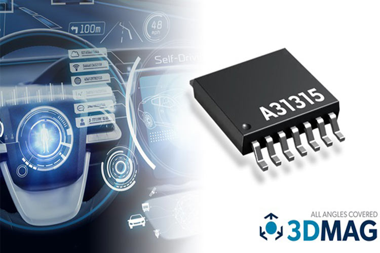
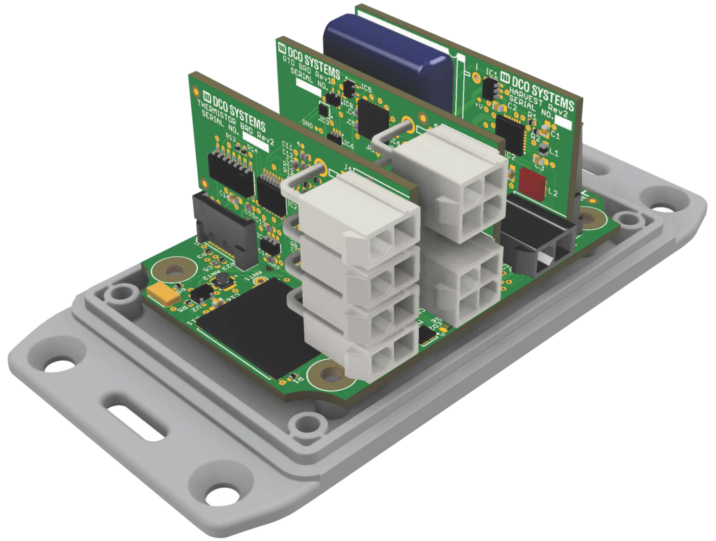
Allegro’s A31315 robust, fully integrated 3DMAG™ Hall effect magnetic position sensors are designed to support a wide range of non-contact rotary and linear position measurements in automotive, industrial, and consumer applications.
This family of sensors integrates vertical and planar Hall effect elements to detect two out of three magnetic field components (X, Y, and Z). Using configurable signal processing, linearization, and angle calculation allows the A31315 sensors to accurately resolve the absolute rotary (full 360° and short-stroke <360°) or linear position of a moving magnetic target.
These A31315 sensors feature ratiometric analog, PWM, or SENT (SAE J2716) interface options to output the angle between the two factory-selected axes or the field from a single axis. In addition, the SENT interface provides the option to output the field measurement from both channels.
Sample Application
Features
3D Hall effect magnetic sensor for absolute rotary and linear position sensing applications
On-chip angle calculation with configurable signal path and flexibility linearization enable customers to achieve the most stringent accuracy requirements while minimizing end of line programming time
Nixie tube is an electronic device for displaying numerals or other information using glow discharge. A potential difference is applied between two electrodes in a glass tube containing low-pressure gas. The flow of electric current through the gas makes plasma. This phenomenon is called glow discharge. First introduced in 1955, the Nixie displays are legendary. The retro nixie displays had a single anode, multiple cathodes that are electrodes shaped like numerals 0-9 stacked on top of one another. Applying the power to one cathode will make that numeral glow. The tube is filled with a low-pressure gas that creates an orange glow discharge. These legendary displays, however, are no longer mass-produced, and they need high-voltage drivers.
There are still some places on the Internet where one can get these retro nixie displays. The high-voltage display drivers are, however, hard to find. The high-voltage driver consists of a DC-DC step-up converter which will step up the voltage level from around 5V to 100-230V.
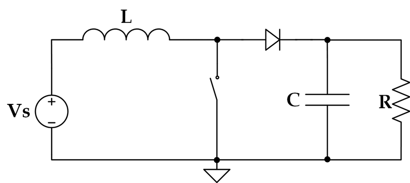
About Step-up Converters
DC-DC step-up converters or boost converters generally consist of a diode, a power MOSFET, and two energy storage elements: an inductor and a capacitor.
When the switch is open initially, there is not much resistance, so high current flows through the inductor. The energy in the inductor is due to the magnetic fields. When the switch is closed, the impedance in the circuit increases and the current will be reduced. The magnetic field previously created will be reduced in energy to maintain the current towards the load. The polarity of the inductor will therefore be reversed and will create another voltage source in series with the input voltage supply. If the rate of switching is fast enough, the voltage will be higher than the input voltage, and this boosted voltage can be controlled by controlling the duty cycle of the switch.
Nixie display drivers also sometimes use flyback converter topology. It provides galvanic isolation between the input and the output with the help of a transformer.
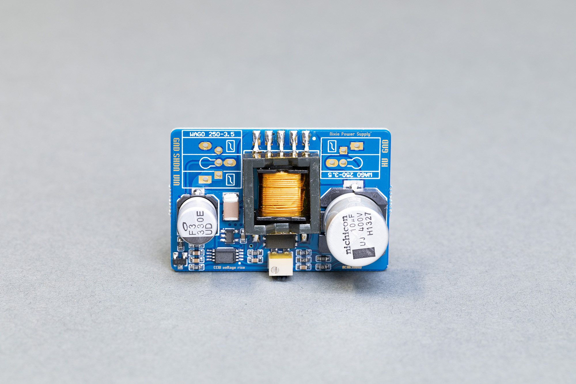
About NCH6300HV HV Power Booster
NCH6300HV high voltage DC-DC power booster is a compact step-up DC-DC converter. It is the updated version of the popular NCH6100HV by Omnixie. As it is a switching converter, its efficiency is high, and heat generation is low. This converter supports input voltage from 3.7V-15V DC and converts it into an output voltage of 100V-230V DC (100mA max @170V). The output voltage is adjustable by a precise potentiometer onboard. The board can be powered by a Lithium battery or by connecting to a USB port as it supports an input voltage of as low as 3.7V. The module can be completely turned off by controlling the SHDN pin for better safety and maximum energy conservation. The board’s output voltage and safety features are perfect for driving the retro nixie displays, as well as other displays like VFD tubes, Magic eye, etc.
The module comes with the PCB terminals and pin headers. Two connectors are present, a 3-pin connector for input and a two-pin connector for the DC output. The pin pitch is 0.1″, therefore compatible with standard perforated boards and breadboards.
The product was successfully funded on Kickstarter on Dec 6th, 2020, and is now on sale at the Omnixie store.
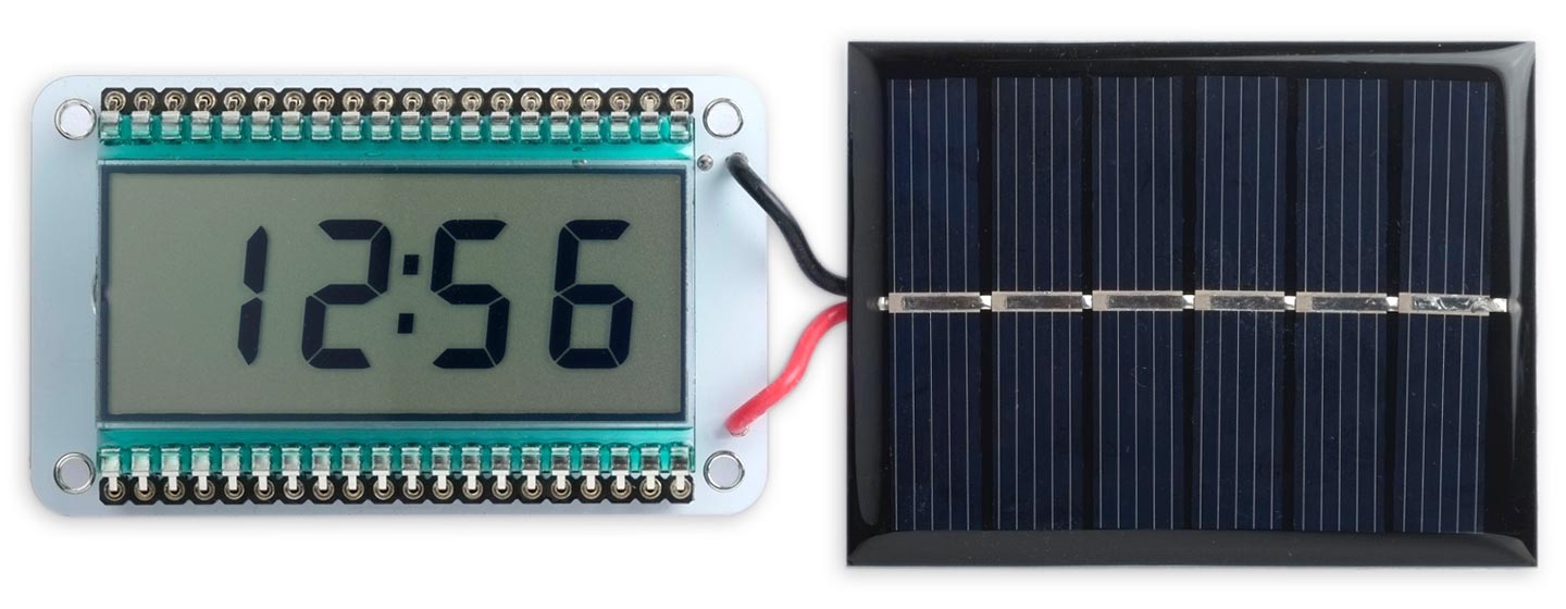
The Liquid Crystal Displays (LCDs) are a type of flat panel display that uses liquid crystals for operation. They are relatively old technology but can be seen in clocks, laptops, computers, calculators, dashboards, and other electronic projects and devices because of their advantages over newer types of displays, including low power, low cost, and readability. Digital LCD watches are quite popular and generally preferred due to their long battery life. David Johnson-Davies recently posted his Low Power LCD Clock in his blog post where he made a very low-power LCD clock, based on an AVR128DA48, capable of running for over three years from a CR2032 button cell or forever from a solar cell.
David used Densitron DG-201208-RP standard LCD for this project. He says,
“I recently bought some Densitron LCD displays on eBay for a few pounds/dollars, and I’d been wanting to try building a low-power clock around them, to see just how low I could get the power consumption.”
The ones used are static displays that can be implemented with independent electrodes for each segment. On the other hand, multiplexed displays are usually implemented with pixels arranged as a matrix consisting of electrically connected rows on one side of the liquid crystal layer and columns on the other side. Each pixel can be activated by intersection. The static display requires 28 individual segment I/O pins, three decimal points, one for colon, and one/two common pin totaling 33-34 pins; plus, there can be some extra display like a minus sign, etc.
“There’s one catch; you can’t use a DC voltage to turn on the segments, because this would cause electrolysis to occur which would slowly degrade the display. The solution is to use AC by switching the polarity across the segment at a low frequency; 32Hz is usually recommended. Fortunately, this is easy to do in software.”
The processor used is an AVR128DA48 in a TQFP-48 package, running at up to 24 MHz and with 128 KB Flash, 16 KB SRAM, and 512 bytes of EEPROM in 48-pin packages. One can also use the lower memory version of these devices as well as ATmega4809 and its lower memory versions which are pin-compatible. David says that the only restriction is that the pins he has used for I2C, PF2 and PF3, only support slave I2C on the ATmega4809. It spends most of its time in sleep mode, for power saving and is turned On by a 64Hz interrupt from the RTC peripheral. The RTC peripheral also keeps time that is controlled by the onboard 32.768kHz crystal oscillator.
The clock also briefly shows the temperature every minute, using the AVR128DA48’s on-chip temperature sensor, and the battery voltage, by using the ADC to read its supply voltage. There is an I2C connection for connection of any other external sensors like the humidity sensor and others.
The clock can run on CR2032 coin cell. Or if you want to power it with a 3V solar panel, there are holes to allow you to fit a 5V supercapacitor in place of the coin cell.
Talking about the power consumption, with a 24MHz clock, it consumes 7.3uA. The CR2032 coin cell of 255mAh would last for about 3.5 years!
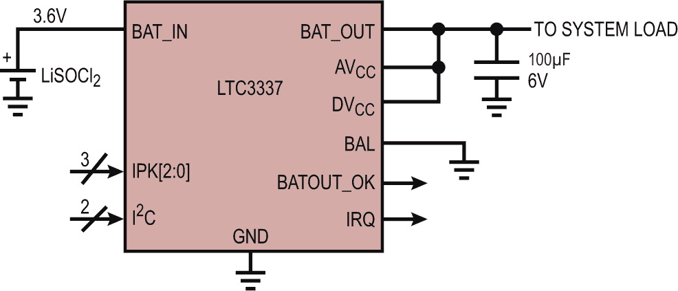
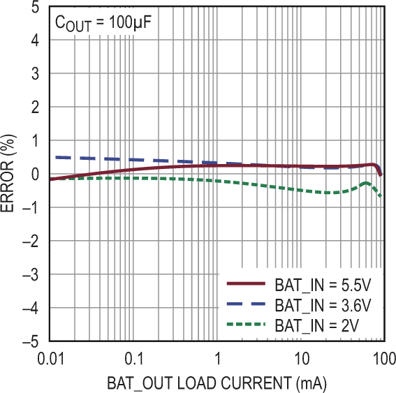
Analog Devices announced a new IC. The LTC3337 is a primary battery state of health (SOH) monitor with a built-in precision coulomb counter. It is designed to be placed in series with a primary battery with minimal associated series voltage drop. The patented infinite dynamic range coulomb counter tallies ALL accumulated battery discharge and stores it in an internal register accessible via an I2C interface. A discharge alarm threshold based on this state of charge (SOC) is programmable. When it is reached, an interrupt is generated at the IRQ pin. Coulomb counter accuracy is constant down to no load.
Additional Monitors for Battery Voltage (V), Battery Impedance (Z), and Temperature (T)
Primary Battery Current (BAT_IN) or Load Current (BAT_OUT) is Counted
Integrated ±10 mA Supercapacitor Balancer
Programmable Coulomb Counter Prescaler for Wide Range of Battery Sizes
Programmable Discharge Alarm Threshold with Interrupt Output
I2C Interface
Tiny 12-Lead 2 mm × 2 mm LFCSP
The LTC3337 also integrates additional SOH monitoring which measures and reports via I2C: battery voltage, battery impedance, and temperature.
To accommodate a wide range of primary battery inputs, the peak input current limit is pin selectable from 5 mA to 100 mA.
Coulombs can be calculated for either the BAT_IN or BAT_OUT pin, determined by the AVCC pin connection. A BAL pin is provided for applications utilizing a stack of two supercapacitors (optional) at the output.
The LTC3337 is offered in a 12-lead 2 mm × 2 mm LFCSP package.
Vishay’s new VCAN36A2 in the SOT-23 and SOT-323 package sizes, and VLIN3333 in the SOD-323 package size, are bidirectional ESD protection devices
Vishay’s new VCAN36A2 in the SOT-23 and SOT-323 package sizes, and VLIN3333 in the SOD-323 package size, are bidirectional ESD protection devices that clamp positive and negative overvoltage transients to the ground. Connected between the signal or data line and the ground, the ESD diodes offer high isolation with low leakage current and capacitance within the specified working range. The VCAN36A2 and VLIN3333 are also available in AEC-Q101 qualified versions.
Key features
VCAN36A2: 2-line ESD protection
VCAN36A2: Working range of ± 36 V
VLIN3333: Small SOD-323 package size
VLIN3333: Working range of ± 33 V
Features for VLIN3333:
For CAN and FLEX bus applications
Small SOT-23 / SOT-323 packages
2-line ESD protection
Working range of ± 36 V
Low leakage current IR of < 0.05 μA
Low load capacitance typical CD of < 10 pF
ESD protection according to IEC 61000-4-2
± 30 kV contact discharge
± 30 kV air discharge
ESD capability according to AEC-Q101:
Human body model: class H3B: > 8 kV
AEC-Q101 qualified versions available
Soldering can be checked by standard vision inspection (AOI = automated optical inspection)
Features for VLIN3333:
For LIN bus applications
Small SOD-323 package size
1-line ESD protection
Working range of ± 33 V
Low leakage current IR of < 0.05 μA
Low load capacitance typical CD of < 13 pF
ESD protection according to IEC 61000-4-2
± 30 kV contact discharge
± 30 kV air discharge
ESD capability according to AEC-Q101:
Human body model: class H3B: > 8 kV
AEC-Q101 qualified version available
Soldering can be checked by standard vision inspection (AOI = automated optical inspection)
FTDI Chip High-Speed USB Bridge ICs with Type-C/PD 3.0 Controllers fully support the latest USB Type-C and Power Delivery (PD) standards. This enables the support for power negotiation with the ability to sink or source current to USB host devices. These high-speed USB bridge devices feature up to two PD ports viz, PD1 port and PD2 port. The PD1 port shares the same Type-C connector with USB data and the PD2 port is the power port only without USB data. The high-speed USB bridge ICs support 5V, 9V, 12V, 15V, and 20V PDO profiles and these profiles are configurable through an external EEPROM at power-up/reset.
The high-speed USB bridges offer up to 40Mbytes/s data rates and multi-channel interfacing. The benefit of a multi-channel bridge is that the system BOM is reduced by removing the need for a USB hub chip. Additionally, each channel of the device appears to the host PC as a separate device. This enables each channel to be independently configured for different modes such as UART, MPSSE, or FIFO. Also, with different parameters such as 4 UARTS all operating with different baud rates.
Features
Supports PD specification Rev 3.0
2 USB PD 3.0 port support:
Port 1 mode configuration for Sink or Dual-role
Port 2 works as Sink, supporting charge through to Port 1
Support 5V 3A, 9V 3A, 12V 3A, 15V 3A, and 20V 3A PDOs as sink or source
Type-C/PD physical layer protocol
PD policy engine using 32-bit RISC controller with 8kB data RAM and 48kB code ROM
PD mode configuration through external EEPROM
Options to use external MCU controlling PD policy through I2C interface
USB 2.0 high speed (480Mbits/second) and full-speed (12Mbits/second) compatible
Adjustable receive buffer timeout
Multi-Protocol Synchronous Serial Engine (MPSSE) to simplify the synchronous serial protocol (USB to JTAG, I2C (MASTER), SPI (MASTER), or bit-bang) design
FTDI royalty-free Virtual Com Port (VCP) and Direct (D2XX) drivers eliminate the requirement for USB driver development in most cases
Highly integrated design includes 1.2V LDO regulator for VCORE and integrated POR function
Low operating and USB suspend current
USB Bulk data transfer mode (512-byte packets in high-speed mode)
Fully assisted hardware or X-On / X-Off software handshaking
Extended -40°C to 85°C industrial operating temperature range
Available in Pb-free QFN-56/QFN-46/QFN-76/QFN-68/LQDP-80 packages (RoHS compliant)
Arduino boards are highly manageable. They are equipped with various sets of digital and analog I/O pins that allow the user to interface with a variety of shields, modules, breadboard circuits, and other circuits. Arduino boards are the brains of many IoT-based projects. For IoT applications, Arduino has released numerous wireless development boards with capabilities like Bluetooth connectivity, WiFi, and RF. One can also interface WiFi, Bluetooth of RF module with standard Arduino boards like Arduino UNO. All these boards, their capabilities, and the Arduino IOT Cloud application make the Arduino environment suitable for major IoT applications. Arduino IoT cloud is an application that aids makers in building connected objects conveniently and securely. With this application, one can connect multiple devices and allow them to exchange real-time data. It has a simple user interface and allows the data to be monitored from anywhere.
“There’s never been an easier way to program your boards or implement device-to-device communication in IoT. Once your devices are hooked up to an IoT Cloud account, they can talk to each other, sync variables, share data, and be combined into powerful dashboards. You even get seamless smartphone control through the Arduino IoT Remote apps.”
Arduino team recently announced in their news article that the Arduino IoT cloud will now support ESP32 devices. ESP32 is series of development boards highlighting low-cost and low power consumption. They employ a Tensilica Xtensa LX6 microprocessor in both dual-core and single-core variations that features integrated Wi-Fi and Bluetooth connectivity for a wide range of applications. Further, ESP32 is highly integrated with in-built antenna switches, RF balun, power amplifier, low-noise receive amplifier, filters, and power management modules. Due to the low power consumption of these devices, they are preferred for mobile devices, wearable electronics, low-power wireless sensor networks, and other IoT applications. ESP32, like Arduino boards, can also interface with other devices through its SPI / SDIO or I2C / UART interfaces.
Thus, adding support for the ESP32 device on Arduino Cloud will aid the makers in their cloud-connected projects. Now, one can use the Arduino cloud taking advantage of the Arduino environment and the low-power consumption of the ESP32 devices.
Arduino team mentions in their news article:
“It’s a huge step forward in bringing IoT devices of all kinds together, and giving them a way to get connected, communicate with each other, and offer new levels of convenience and control.”
Support for the ESP8266 devices is already available in the free Arduino cloud tier. The team says that the addition of ESP32 support and along with various cloud-compatible Arduino devices adds some serious power to a cloud account.
For connecting your ESP32 board to the Arduino cloud, you can get started with the free plan. You will then need Arduino Create Agent that lets Arduino IoT Cloud detect and communicate with supported boards. It also allows uploading sketches from your web browser using the Arduino Web Editor IDE. For using ESP32, create a device and select “ESP32 device” and set up the device with the normal process.
The Arduino team says about the impact of this step,
“This is a great way to upgrade existing projects, home automation, or other applications. It makes it so easy to take advantage of IoT Cloud’s powerhouse features. With almost no code, you can have any combination of Arduino, ESP8266, and ESP32 boards communicating and working together seamlessly and wirelessly. It’ll cut the time it takes to build adventurous new projects while expanding the possibilities and significantly reducing the legwork.”
Supercapacitors, ultracapacitors, and electric double layer capacitors. No matter to which they are referred, this passive electronics component has some very desirable properties for the Internet of Things (IoT), smart wearables, and energy harvesting markets. Supercapacitors are ideal for providing efficient power pulses for transmitting data and rapidly collecting energy from intermittent sources, and to top it all off, allow for a near infinite cycle life, preventing the need to stress over battery management and replacement. However, traditional rigid, cylinder- and rectangular-shaped supercapacitors unnecessarily limit product design as they are restricted to use on a circuit board or are so large they need a dedicated storage space in which the component may reside. In IoT devices, they use about ~50% of the surface area (space) available on the printed circuit board (PCB).
A plethora of modern programmable chips, electronic components, and sensors are available in sizes comparable to as small as grain of sand to only as large as a dime. In relation, energy storage components, such as batteries and supercapacitors, are thousands of times larger and make up the bulk of design intent. This creates a “tail-wagging-the-dog” constraint. The active electronics should dictate the size of the PCB, not the passive energy storage devices and components. All too frequently the energy storage device prevents flexibility in the size and shape of the final product, inhibiting the opportunity for product miniaturization and/or product improvement.
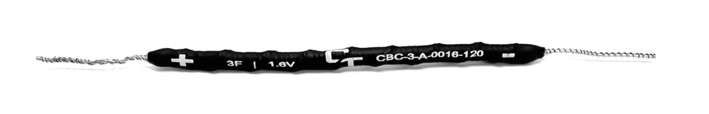
Capacitech’s Cable-Based Capacitor (CBC) innovation, which may be found on their website, dramatically improves the form factor of supercapacitors offering a thin, flexible, and wire-like shape, allowing the CBC’s to be used in cabling infrastructure and mechanical arrangements where the traditional cylinder, rectangular, or even flat supercapacitors are unable to fit. It can be used to streamline product design and offer features that are not possible with a traditional supercapacitors. It seems simple, but implementing CBC technology in the wiring harness of a product or around a PCB rather than on the face of a PCB will free quite a bit of “real estate,” so to speak.
The power pulses are a supercapacitors strongest asset and may be used for more than just transmitting bits of data or conspicuously collecting data. These power pulses are also ideal in robotics for movement and adjustment. In particular, actuators at joints require these intermittent bursts of power. This information is all related and useful as discussed on Capacitech’s website in their most recent blog post. Exoskeletons are making a surprise, but necessary, appearance in many industries which require a notable amount of physical labor. These robotic fixtures may have the CBC technology implemented around, across, and within the wiring infrastructure of many of the actuator devices, minimizing the size of them around joints and inadvertently, decreasing weight, all due to the ability to flex with the exoskeleton as it moves. Not to mention the improved stability and strength applications allowing those utilizing this technology to comfortably lift more, improve endurance, and prevent injury by increasing safety. This wearable technology has the potential to be the future standard issue equipment for warehouse workmen, first responders, and even military members, and the CBC has the potential to improve this technology even further.
The exoskeleton may even double has not just a wearable device that may be improved by the CBC, but also an energy harvesting device in and of itself. The use of piezoelectric energy harvesting could be utilized through the bending and movement of the joints where the actuators are housed, such as what is used by Bionic Power. The friction and movement will allow for charging capabilities, and the near infinite cycle life of supercapacitors only further amplifies the destined combination of these components.
Let’s take a biofeedback shoe as another example. MIT made a great demonstration, and posted on their Technology Learning Office website, of how energy harvesting in footwear could be leveraged, but their design features a large supercapacitor hanging off the boot. Traditional supercapacitor shapes and form factors would destroy the streamlined look of a shoe. On the other hand, a thin and flexible supercapacitor like the CBC can be distributed throughout the shoe where it can remain discrete and is comfortable to the user.
The accelerometer, processor and Bluetooth modules are tiny enough that you could easily hide them in the tongue of the shoe. Companies, like BeBop Sensors, have even integrated pressure sensors into soft textiles that the user can stand on. Unfortunately, a hard and rigid supercapacitor, which could be charged by biomechanical (kinetic) energy from electroactive polymers harvested from the user’s motion, is hard to fit anywhere without creating discomfort for the user or an unsightly bulge.
These CBC’s are flexible enough that they can be integrated into the structural elements of a design, rather than be in intimate contact with the rest of the electronics on a circuit board. As a further example, a helmet that detects dangerous blows to the head can have the CBCs worked into the lining of the helmet. This would allow for more even weight distribution and a thinner, more streamlined shape than is possible with traditional supercapacitors.
Other wearables, jewelry, or medical monitoring applications run into similar problems, as discussed by Capacitech here. The solution is a supercapacitor that is flexible and seamlessly integrated into alternative parts of the product or system where space is more abundant than on the circuit board. Not to mention, these applications may also invite the use of small, photovoltaic (solar) devices to be used to harvest energy for these supercapacitors, creating a dynamic duo of electronic components.
With the development of smart technology and improved monitoring systems, more and more distinct issues continue to arise. Reliable power sources may be unavailable or in difficult-to-reach places such as underground rail systems or attached to the highest rafters or near dangerous equipment in a manufacturing warehouse. As discussed in yet another blog post by Capacitech Energy here, batteries often do not last the life of sensors or other equipment and need regular maintenance. A technology being continuously developed to combat the issues of battery management and replacement is through photovoltaic and piezoelectric energy harvesting sources, as mentioned above.
The goal is to complement or remove batteries due to their short service life, which means an energy storage element is necessary to ensure proper application. The CBC is capable of long service life as a supercapacitor with flexible physical properties and can provide the peak-power needed to collect and/or transmit data.
When designing any product, consider what can be accomplished with flexible supercapacitors and the space they save on circuit boards. In using a supercapacitors that takes less surface area on PCBs, or offsetting supercapacitors from the PCB to the infrastructure of the system, design engineers can make their products smaller, offer new features, and increase performance to help set themselves apart from the competition. The CBC is optimized to use less surface area on PCBs than other supercapacitors. It can also be used off the circuit board entirely and inside another piece of infrastructure, such as a wiring harness or between cracks of foam in a protective helmet, among other places.
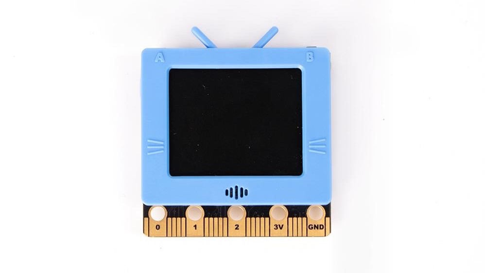
We have already seen hardware coming into the market that is specially designed for students and newcomers to develop IoT-based applications. Top embedded device manufacturer Arduino and BBC micro:bit have been in the space of inspiring children and making easy and practical learning. Continuing to curate exceptional learning materials through hardware and easy-to-use software, we have KittenBot releasing its new hardware based on the ESP32 microcontroller, enabling students to deploy AI and IoT-based applications effectively.
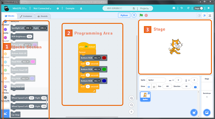
The all-new KittenBot Future board comes with a decently sized 160×128 full-colour TFT screen allowing users to explore the capabilities of the hardware through real-time visual feedback that can be sensor readings. Many students are fascinated by how smart home appliances work. To help them demonstrate simple projects, the KittenBot Future Board comes with support for Wi-Fi and Bluetooth wireless networks. Utilizing these, the newcomers can easily deploy working projects. To do so, we have already seen some block programming tools available in the market. Similarly, we have KittenBot’s Scratch3.0 graphical programming software to make it more interesting for students.
This doesn’t restrict the user to only IoT applications but also works on AI-based projects. Thanks to the onboard speech recognition module that can now work with the Chinese and English language. Along with this, the module also comes with a speaker and LED lights, giving it an aesthetic look with audio-visual feedback. You can now store multiple programs for different projects on the onboard storage that can be expanded with the optional SD card slot. The manufacturer has also provided a light and temperature sensor along with the buzzer that makes it very cost-efficient. Not only this, but if there are several KittenBot Future Boards working together, then they can easily communicate with each other through wireless radio.
The Kittenblock Graphical programming software
KittenBot has provided the board with a Type-C USB interface to power the board, but those who already own a rechargeable 3.7V Lithium battery can also use it. This light-weight, easy-to-use AIOT Python Education Kit is now sold for $29.99 on the official product page.
The light-emitting diode commonly referred to as LED is a special type of diode with characteristics similar to that of a normal diode. The LED is a device that converts electrical energy into light energy. The LED is a current-driven semiconductor device and when forward-biased emits light of narrow bandwidth depending on the construction of the LED. The emitted light may either be in the visible or non-visible spectrum. LEDs can be categorized as the most widely used semiconductor devices and are mostly used in televisions, colored displays and in road lights, etc.
The LEDs are fabricated to have thin layers of heavily doped semiconductor materials. The semiconductor material and its doping level characterize the emitted light when forward-biased. The different semiconductor materials and the doping levels emit light of different wavelengths. The emitted light in the form of photons is the energy released by the conduction electrons when they recombining with the holes of the valence band. Whilst recombining, a sufficient amount of energy is released to produce monochromatic light by photon.
Physical Construction
The physical appearance and construction of LEDs are different from that of the conventional diode. Normally, the PN junction of a LED is covered by strong transparent epoxy resin having a hemispherical shape. This construction not only helps in protecting the delicate construction of LED but also acts as a lens to concentrate/ focus the emitted light. The light emitted by the PN junction is not of significant strength and would reflect away unnoticeable. However, the construction of domed shaped cover helps the light to focus, strengthen, and to be more prominent.
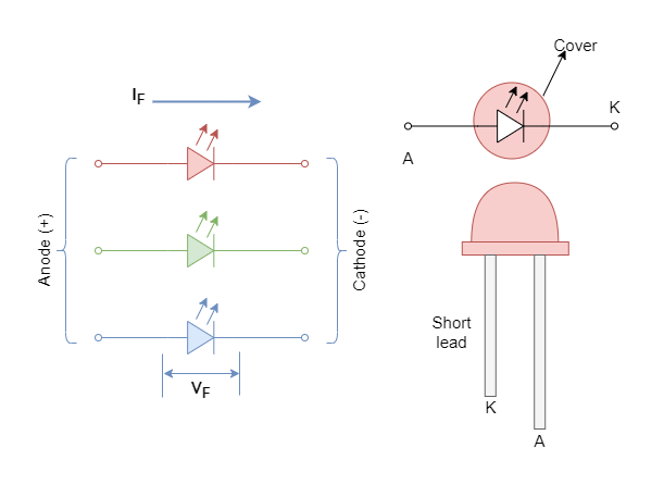
The LEDs with monochromatic light have two legs i.e. anode (+) and cathode (-). The cathode of an LED can be identified by either a flat surface/ notch or by shorter lead. The LEDs are replacing conventional light bulbs because of their efficiency and construction size. The conventional light sources dissipate heat and losses much of the energy whilst LEDs do not heat up producing minimum voltage drop across them. Being an electrostatic device, the LED can be constructed into very small sizes and shapes depending on the application requirements.
Figure 1: The LED symbol and typical shape
Composition of Light Emitting Diode
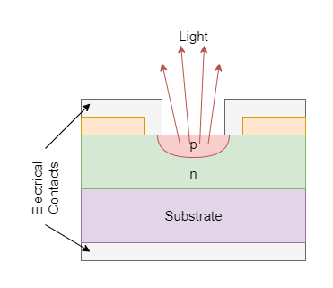
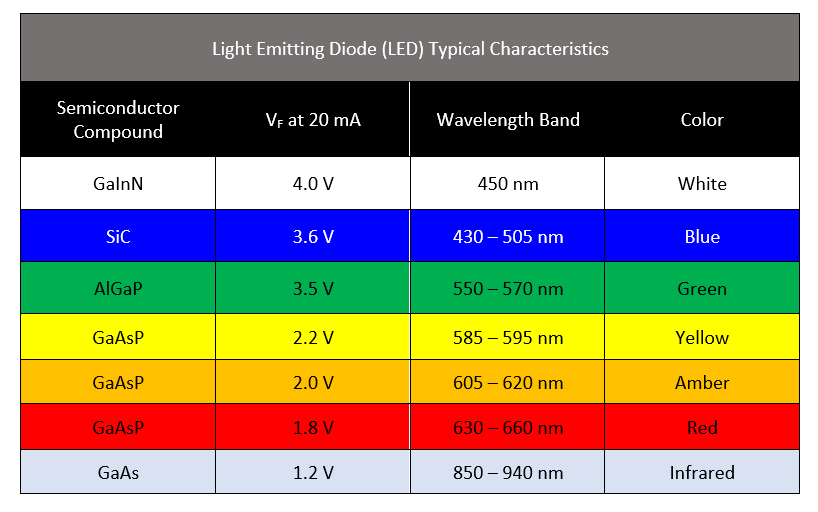
The composition of the PN junction is selected in a such way to emit a specific wavelength/ color and, as such, the semiconductor materials are deliberately chosen to attain this. The semiconductor materials used in conventional diodes are Silicon and Germanium, whereas, in LEDs, the semiconductor compounds are used such as Gallium Phosphide (GaP), Silicon Carbide (SiC), Gallium Arsenide Phosphide (GaAsP), Gallium Arsenide (GaAs), or Gallium Indium Nitride (GaInN), etc. These compound semiconductors are made by mixing semiconductors in certain ratios/ mixtures to strengthen a specific wavelength.
Figure 2: The LED Composition layers
The different compounds and mixing ratios produce light of specific bandwidth in the light spectrum and also characterize the intensity of light emitted.
From the above chart, it is clear that what color is emitted by which semiconductor compound and its wavelength. The LED’s cover is usually made of color belonging to emitted light by the PN junction. It is merely to indicate light the color of LED and, additionally, to enhance the output of emitted light.
The most common and cheaply available colors are Red, Green, and Blue which are the primary colors easily produced by semiconductor compounds. Other colors are expensive and are produced by mixing the primary colors.
Types of Light Emitting Diodes
Gallium Arsenide (GaAs): Infrared
Gallium Arsenide Phosphide (GaAsP): Red, Infra-red, and orange
Aluminium Gallium Arsenide Phosphide (AlGaAsP): Red (Bright), orange, and yellow
Gallium Phosphide (GaP): Red, yellow and green
Aluminium Gallium Phosphide (AlGaP): Green
Gallium Nitride (GaN): Emerald green
Gallium Indium Nitride (GaInN): Ultraviolet, green (bluish), and blue
Silicon Carbide (SiC): Blue (substrate)
Zinc Selenide (ZnSe): Blue
Aluminium Gallium Nitride (AlGaN): Ultraviolet
Voltage Drop and Series Resistance
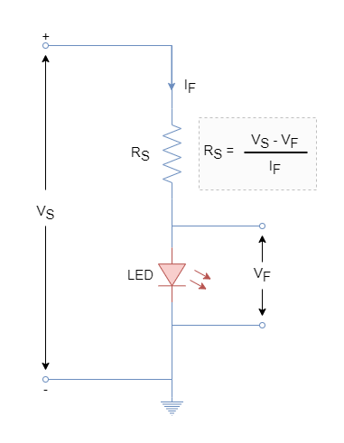
Similar to conventional diode, the LED is current driven and a certain voltage drop occurs when put in forward-biased mode. The forward voltage drop (VF) ranges from 1.2V to 4.0V and is dependent on the type of compound material is used in the LED. The LED emits a light when a voltage greater than the forward voltage drop is applied and the current flows through it. The excessive current flow can damage the sensitive PN junction of LED and as such requires that a proper series resistance be inserted in between the LED and voltage source. The value of series resistance should be such that it does not permit more than 80% of the rated current of the LED and should permit a sufficient amount of current to significantly brighten the LED.
Figure 3: Single LED in series with the resistance
A Single LED Example
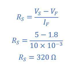
The value of series resistance can be determined using Ohm’s Law. For this purpose, the forward voltage drop (VF), forward current (IF), and supply voltage (VS) should be known. For example, for a red color LED: VF = 1.8 V, forward current limited to IF = 10 mA and voltage supply VS = 5 V. Then value of series resistance (RS) required for the red LED is:
The standard value resistance of 330 Ω is suitable for the selected red LED. The higher valued resistance is selected than the calculated one to remain under the safe limit of forward-current.
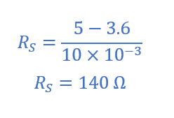
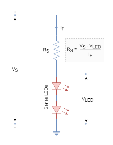
Multiple LEDs
The multiple LEDs can be connected in series and as such driving current will be the same for the LEDs in series. However, for the selection of series resistance, voltage drop (VF) for each LED must be considered. For example, a two red LED circuit will drop a voltage of 2 X 1.8 = 3.6 V and series resistance (RS) should be calculated as follow:
For two LEDs, a series resistance of 140 Ω is required to provide 10 mA of driving current.
Figure 4: Multiple LEDs in series with the resistance
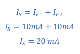
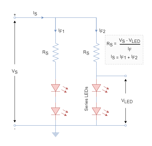
Similarly, a series and parallel combination of multiple LEDs can be made. Another branch of two red LEDs can be added in parallel to the previously constructed circuit to have a total of four LEDs driven by the same power source. The current in each branch will be same i.e., IF1 = IF2 = 10 mA. However, the source current (IS) will be doubled to drive the four LEDs.
Figure 5: Multiple LEDs in series and parallel configuration
Controlling LEDs
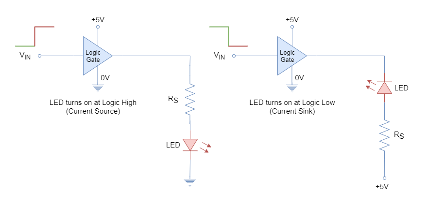
The LEDs can be controlled i.e. turning ON & OFF through a number of ways. Mostly, LEDs are used in low voltage digital circuits where they are driven by microcontrollers or logic gates. The logic gate or microcontroller pin can act as input or output. When the pin is set as output it acts as a current source and as a sink in input type. The capability of current handling as source or sink varies and may range from 20 mA to 50 mA. This also indicates that a series resistor is mandatory for the digital circuit to avoid damaging the LED.
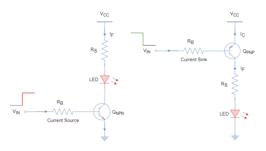
In the following figure, a TTL or CMOS logic is used to drive a LED. The value of the series resistor can be calculated in the same way described earlier. The logic gate is connected to LED as a source as well as a sink in the figure.
Figure 6: Driving LEDs through digital circuits
When the cathode of LED is connected to the ground and anode to the logic circuit through a resistor. Then a logic high will turn ON the LED and vice versa. The logic gate is acting as a source in this configuration. On the other hand, when an anode is connected to logic high voltage through a resistor and cathode to the logic circuit then a logic low will turn ON the LED and vice versa. Digital gate acting as a sink in this configuration.
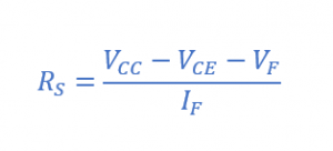
However, due to the power and current handling limitations of logic circuits, a few of the LEDs can be connected directly to them. The external/ isolated circuitry is required to drive a large number of LEDs such as those used in bigger LED displays. A discrete component such as a transistor is used to drive fast-switching LEDs. The rating of the transistor can be carefully selected depending on the LEDs to be driven.
In the following figure, the NPN and PNP transistors are used to drive the LED from a microcontroller or a logic circuit. The series resistor is to be calculated using the following formula:
Figure 7: Driving LEDs through digital circuits isolated by transistors
The logic high and low driving circuits using transistors are shown. The logic source is connected to the base of the transistor and switches ON & OFF the transistor depending on the logic and circuit. The switching ON of the transistor in active mode will complete the LED circuit and turns ON the LED.
Multi-colored LEDs
The single-color LEDs are most commonly used for indications purposes or in seven-segment displays. They are low cost due to simple construction and are available in different sizes & shapes. Besides single-color LEDs, the bi-color and tri-color LEDs are also most commonly used to display different states such as power or battery level, etc.
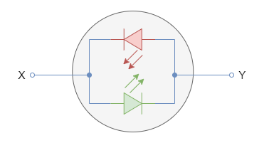
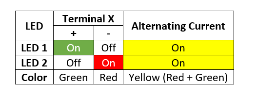
A bi-color LED has two different color LEDs connected in inverse-parallel configuration. The bi-color LED has two terminals and supply from either side produces a color. The reversal of polarity changes the color produced by the LED. These are used for checking battery polarity terminals or other indications etc.
The alternating or bidirectional current applied to it turns ON & OFF both LEDs at a considerably high rate. The switching is undetectable by the naked eye and hence a mixture of both colors is observed.
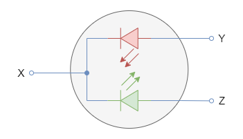
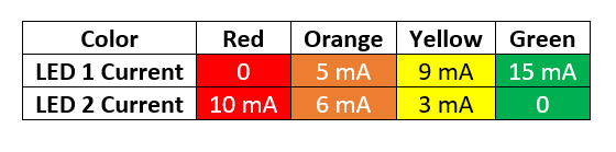
A multi-colored LED comprises red and green LEDs which are connected in parallel to each other. The color emitted by the compound LED is dependent on the driving current of both individual LEDs. The emitted color is the combination of both individual LEDs and their driving current source. The following figure shows a multi-colored LED and its driving current color table.
Applications
Indication purposes.
Seven segment displays for displaying numbering data.
Handheld devices, flat-screen LED televisions, and large-screen displays for advertisement.
Infrared-driven devices such as remote controls.
Opto-couplers
Conclusion
A light-emitting diode converts electrical energy into light energy.
A light-emitting diode is a type of special diode whose PN junction is made from a compound semiconductor.
The LED comprises of heavily doped semiconductor and has a very thin layer of PN junction.
The forward-biased LED enables the electrons in the conduction band to recombine with the holes in the valence band. In doing so the electrons release the energy in form of photons/ light.
The color emitted by the photons is dependent on the semiconductor compound used in the LED and its intensity is dependent on the forward biasing current.
The wavelength of the emitted color lies in the visible or invisible light spectrum.
The series resistance is used essentially to avoid damaging the LED(s) and the value of series resistance requires to be calculated depending on the LED type, number of LEDs, and their series/ parallel configuration.
The LEDs are available in a variety of colors. The monochromatic colors are widely used and cheap. Whereas, bi-color and multi-color LEDs are also available but comparatively costly.
The LED applications include, but not limited to, indication purposes, displays, televisions and large advertisement displays, etc.