DC-DC converters are needed in almost every commercial product, whether it is industrial, medical, defensive, automotive, or any other application. These converters are electronic circuits that can convert the DC voltage from one level to another. There are two types of DC-DC converters: linear and switching converters. Linear converters are resistive which means that they use resistive voltage drop to create a regulated output voltage. This also means that the input voltage should always be higher than the input voltage, and linear converters can only step down a voltage level. On the other hand, switching converters perform the conversion by storing the energy periodically in the energy storage elements like capacitors and inductors. The stored energy is then provided to the load at the desired voltage level.
There are several benefits of switching converters. Firstly, switching converters are highly efficient. They have an efficiency in the range of 80-90%. Moreover, the buck-boost converters can step up and down the voltage levels to maintain the output voltage. Additionally, thermal management is simplified due to lower losses.
SEPIC
SEPIC (Single Ended Primary Inductor Converter) type of converter is very similar to the traditional buck-boost converters. SEPIC can step up as well as step down the voltages accordingly. The simple buck-boost converters consist of two MOSFETs used as switches. SEPIC converters, however, are characterized using two inductors, one of them is at the input that is for coupling, and another one is connected to the ground.
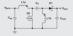
The SEPIC topology consists of an input capacitor, an output capacitor, coupled inductors, a diode, and a power MOSFET. To understand the working of the SEPIC, let’s assume that the switch is first open. In this state, it can be easily seen that the input capacitor Cin is charged at the input voltage. The voltage across the inductor L1b must be the same as Vout and therefore, the voltage across the switch must be Vout+Vin.
When the switch is closed, the capacitor Cp is charged to the input voltage which then charges L1b. Energy is also stored in the inductor L1a from the input during this state. When the switch is opened again, the inductor L1a discharges to the output capacitor via diode and power the load.
The converter’s output voltage can be controlled by adjusting the duty cycle of the MOSFET. SEPICs are mostly controlled by PWM regulator ICs and a microcontroller that drives the gate of the MOSFET according to the sensed voltages. But for compact devices, DC-DC converter ICs are widely used. They consist of integrated MOSFETs, an internal voltage reference for feedback, and are highly efficient.
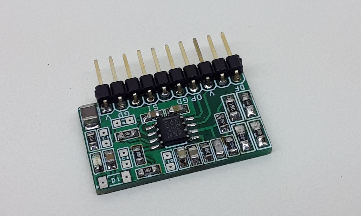
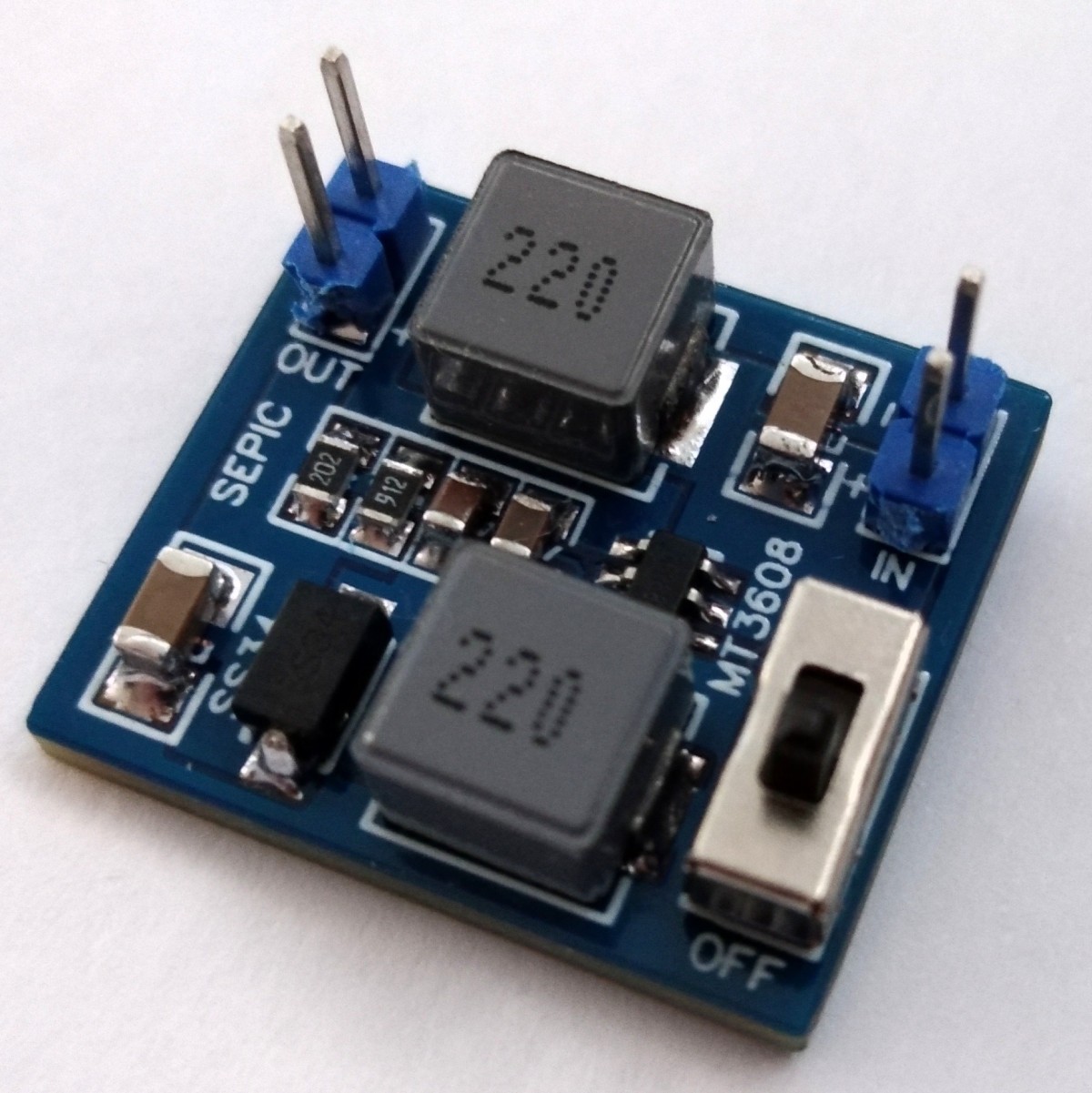
SEPIC PCB based on MT3608
Stefan Wagner from Germany designed a SEPIC PCB based on MT3608 DC-DC converter IC. MT3608 is a very compact boost converter IC that provides up to 97% efficiency and also allows a wide input voltage range. In addition, MT3608 includes under-voltage lockout, current limiting, and thermal overload protection to prevent damage in the event of an output overload. The schematic of the SEPIC design is as follows:
-
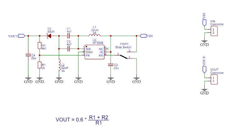
Source: https://github.com/wagiminator/Power-Boards/blob/master/SEPIC_MT3608/SEPIC_MT3608_schematic.pdf The output voltage is divided by a resistive voltage divider to the FB pin of the IC. The voltage at the FB pin is compared to an internal reference voltage of 0.6V, and the PWM is controlled accordingly.
The complete project including the Gerber files, performance results and BOM can be found at https://github.com/wagiminator/Power-Boards/tree/master/SEPIC_MT3608