Programming TPI AVRs using USBASP Programmer

AVR microcontrollers are RISC architecture-based microcontroller series that have on-chip flash memory for data storage. The popularity of ARM microcontrollers can be seen by the range of applications it has. They are used in home automation, touch screen, automobiles, medical devices, and defense. They are also quite popular among hobbyists and makers. Most AVR microcontrollers use the In-System Programming (ISP) feature. ISP is a feature of microcontrollers that allows uploading of a program while the chip is on the system. This aids the end-users as they can program the hardware device according to their needs. Three pins are dedicated for the programming which are Serial Clock (SCK), Master-In-Slave-Out (MISO), and Master-Out-Slave-In (MOSI). All types of memory on the micro-controller can be accessed using the SCK, MISO, and MOSI pins while holding the RESET pin LOW.

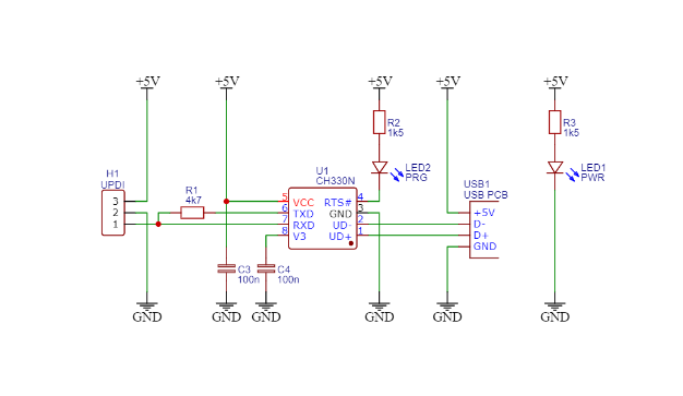
USBASP is an open-source ISP (In-System Programming) programmer for AVR devices. If someone wants to develop programs that use the UART of Atmega32, you need to upload code using ISP. USBASP can be used for programming other AVR micro-controllers also. It can be used for burning the boot loader. The LED on the board indicates power. It goes off while uploading code, giving an additional indication. Newer AVRs use much faster programming techniques like TPI and UPDI. But someone may want to flash newer TPI-based AVR microcontrollers with an old USBASP board. Kevin Cuzner documented how to program TPI-only AVR microcontrollers using a USBASP device.

TPI Programming: A summary

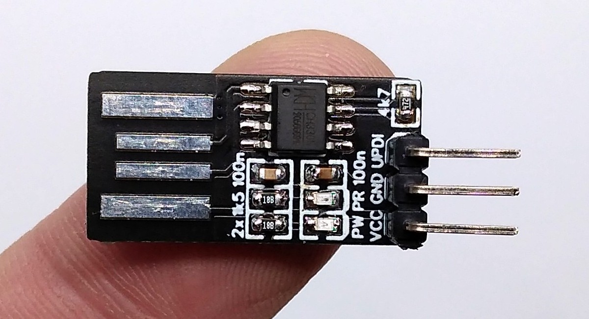
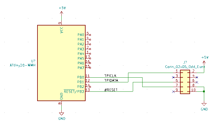
Before going into the steps involved in the programming process, let’s first get an overview of TPI programming. The Tiny Programming Interface (TPI) is the only programming interface available in some newer AVR microcontrollers. TPI interface method consists of two layers Physical layer and the Access layer. The physical layer consists of two operations: transmit and receive. The TPI Access layer controls the mode of operation. TPI interface method needs only 3 pins for usage which are Reset, TPIDATA, and TPICLK. TPIDATA is a bidirectional data line unlike in the SPI method, where 2 data lines are used for transmission and reception of data.

Steps to program TPI based AVR MCUs using USBASP programmer

Kevin listed the following steps that are involved in programming TPI-only AVR MCUs using USBASP:

  1. Buy another USBASP programmer as one of them will be the programmer and another one would be the target that is going to become TPI capable.
  2. Download the latest firmware from Thomas Fischl’s website: https://www.fischl.de/usbasp/
  3. Switch the programming jumper on the target by shorting the appropriate header (sometimes labeled JP1, sometimes labeled JP2). It’s a two-pin jumper and is NOT the target voltage jumper, nor the “slow clock” jumper.
  4. Connect the programmer USB to the PC. Don’t connect the target to the PC.
  5. Connect the two USBASPs using the 10-pin ISP ribbon cable.
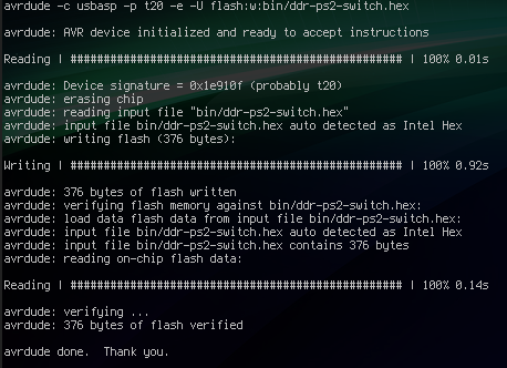
  6. Use avrdude to program the downloaded firmware (be sure to choose the correct hex file for the ATmega used on the target programmer).

For interfacing, connect the TPIDATA pin of the TPI header to the MOSI pin of MCU, TPICLK to ISP CLK, and RESET to the corresponding RESET pin. Further, it is necessary to ensure that the AVR is running at 5V.

Source: http://kevincuzner.com/2020/11/08/avr-tpi-programming-with-usbasp-for-dummies/

Complete documentation can be found at http://kevincuzner.com/2020/11/08/avr-tpi-programming-with-usbasp-for-dummies/

MAX17227A is a 2 A nanoPower boost converter

Maxim’s MAX17227A is a 400 mV to 5.5 V input, 2 A nanoPower boost converter with short-circuit protection and True Shutdown™

Maxim’s MAX17227A is a nanoPower boost converter, capable of delivering a load up to 2 A peak inductor current and providing True Shutdown, cycle-by-cycle inductor current limit, short-circuit, and thermal protection. During shutdown, current drawn from the input pin is 1 nA. The MAX17227A offers ultra-low quiescent current, small total solution size, and high efficiency throughout the load and line range. These features make it ideal for battery-powered applications where extended battery life is required and high efficiency is necessary at all power levels.

Features

  • 350 nA quiescent supply current from output
  • Output short-circuit protection
  • True shutdown mode: 1 nA shutdown current
  • 96% peak efficiency, 90% or higher at 500 µA

more information: https://www.maximintegrated.com/en/products/power/switching-regulators/MAX17227A.html

MP6540H/MP6540HA are three-phase brushless DC motor drivers

MPS’ 50 V, 5 A and 6 A, three-phase power stage drivers offer PWM and enable inputs

The MP6540H and MP6540HA from Monolithic Power Systems are three-phase brushless DC motor drivers. These devices integrate three half-bridges consisting of six N-channel power MOSFETs, pre-drivers, gate drive power supplies, and current-sense amplifiers. The MP6540H has enable (EN) and PWM inputs for each half-bridge, while the MP6540HA has separate high-side (HS) and low-side (LS) inputs, otherwise they are identical. The MP6540H can deliver up to 6 A of peak current and 5 A of continuous output current, based on thermal and PCB conditions. The MP6540H uses an internal charge pump to generate the gate drive supply voltage for the high-side MOSFETs, and a trickle charge circuit that maintains sufficient gate drive voltage to operate at 100% duty cycle. Internal safety features include thermal shutdown, undervoltage lockout (UVLO), and overcurrent protection (OCP). The device is available in a QFN-26 (5 mm x 5 mm) package.

Features:

  • 5.5 V to 50 V operating supply voltage
  • Three integrated half-bridge drivers
  • Maximum 5 A output current, 6 A peak current
  • MOSFET ON resistance: HS + LS 45 mΩ
  • MP6540H: PWM and EN inputs; MP6540HA: HS and LS inputs
  • Internal charge pump supports 100% duty cycle operation
  • Automatic synchronous rectification
  • UVLO and thermal shutdown protection
  • OCP
  • Integrated bidirectional current-sense amplifiers
  • Available in a QFN-26 (5 mm x 5 mm) package

more information: https://www.monolithicpower.com/en/mp6540h.html

Vishay VEML6031X00 high accuracy ambient light sensor supports I2C BUS

The Vishay Semiconductors’ VEML6031X00 high accuracy ambient light sensor supports an easy-to-use I2C bus communication interface

The Vishay Semiconductors’ VEML6031X00 high accuracy ambient light sensor supports an easy-to-use I2C bus communication interface and additional interrupt feature. The ambient light result is available as digital value. The VEML6031X00 is ideal for automotive applications, including display backlight controls, infotainment systems, rearview mirror dimming, interior lighting control systems, and head-up displays.

Key features

  • High accuracy ambient light sensor supports an easy-to-use I2C bus communication interface
  • 16-bit resolution sensor in a small opaque 2.67 mm x 2.45 mm package
  • Incorporates a high sensitive photodiode, a low noise amplifier and a 16-bit A/D converter
  • Surface-mount package type

Additional features

  • Ambient light sensor (ALS) integrated modules
  • 2.5 V to 3.6 V supply voltage range (VDD)
  • Communication via I2C interface
  • Multiple I2C Slave address options available:
    • VEML6031X00: 7-bit I2C Slave address 0x29
    • VEML60311X00: 7-bit I2C Slave address 0x10
  • 1.7 V to 3.6 V I2C bus H-level range
  • Floor life of 4 weeks, MSL 2a, according to J-STD-020
  • Low shut down current consumption of typ. 0.5 μA
  • Compact dimensions (L x W x H):
    • 2.67 mm x 2.45 mm x 0.6 mm
  • AEC-Q100 qualified

more information: https://www.vishay.com/ppg?80007&designtools-ppg

Fibocom to Accelerate Digital Transformation in IIoT with 5G Connectivity

World Telecommunication and Information Society Day (WTISD) takes place on May 17th every year, to connect the world and promote digital technologies. This year, the theme is to Accelerate Digital Transformation in challenging times. As time goes by, people started to realize the inconvenience of conservative manufacturing as well as the urgency of digital transformation, especially after the COVID-19 crisis. Thus, both governments and the private industrial sectors have turned to IIoT as a better solution for smart manufacturing in this changing time.

How Can IIoT Help?

IIoT (Industrial Internet of Things) offers innovative ways to boost operational efficiency and introduce a new wave of industrial services. IIoT, also known as Industry 4.0, brings together Connectivity, Data & Computational Power, Analytics & Intelligence, and Human-Machine Interaction. It is the network of a variety of industrial devices connected by telecommunication technologies, enabling the systems to monitor, collect, exchange, analyze as well as deliver data.

Connectivity, Data & Computational Power

Connectivity is the foundation of Industry 4.0 and part of the foundational technologies applied along the value chain. This is achievable with the help of the high capacity, high speed, low latency and reliable 5G network. 5G ensures the delivery of IIoT technologies and helps keep all machines and robots perfectly in sync in real-time.

Analytics & Intelligence

IIoT achieves incredible levels of efficiency, productivity, and performance by integrating machine-to-machine communication with industrial data analytics. For example, industrial AI inside a refinery pipe can detect corrosion to provide real-time production data, allowing a factory to reveal extra capacity. Another example of IIoT intelligence is digital twin. It allows computers to “tell” operators how to maximize productivity or predict a malfunction before it happens, potentially saving billions of costs.

Human-Machine Interaction

To transform form traditional, labor-intensive manufacturing processes to modern, autonomous ones, the adoption of smart manufacturing fits in the future roadmaps of hyperautomation. For instance, AGV (Automated Guided Vehicle) is indispensable for smart warehousing and smart factories, fully utilizing space and labor resources. When human operates at the ordering systems, AGVs will receive signals and carry required items to the picking workstations. HD video of the factory floor from a camera attached to an AGV can also be streamed with the help of 5G. AGV helps to realizes human-machine interaction and is the best choice for manufacturers to save energy, reduce costs, and increase productivities.

Fibocom Wireless Solutions

IIoT requires stable wireless communication network coverage and fast inter-AP roaming switching to ensure efficiency and stability in various industrial scenarios. Fibocom has been an active player in the sector of IIoT, helping to accelerate digital transformation around the world. Fibocom provides one-stop IoT (Internet of Things) services including wireless communication modules and IoT application solutions. Whether it is to improve production efficiency or to reduce management costs, Fibocom is capable for offering 5G connectivity with faster transmission speed, better carrying capacity, and lower network latency, demonstrating the huge application potential of 5G in IIoT.

Fibocom’s 5G wireless communication modules are designed to offer eMBB (enhanced Mobile Broadband), URLLC (Ultra Reliable and Low Latency Communications), as well as mMTC (massive Machine Type Communications). Supporting 5G standalone network (SA) and non-standalone (NSA) network architectures, Fibocom 5G wireless module series supports the Sub-6GHz and mmwave bands, and is compatible with 5G NR, LTE and WCDMA standards. It eliminates customers’ investment concerns at the initial stage of 5G construction, responding to the commercial demand for rapid landing. Meanwhile, Fibocom 5G modules come with a rich set of interfaces including USB3.1 (3.0), USB2.0, PCIe3.0 (2.0), SPI, SDIO, GPIO, UART, etc. It has been certified by various regional operators, industry associations and local regulation, satisfying different deployment requirements for customers worldwide.

Industrial digital inputs with the MAX22191

App note from Maxim Integrated on their parasitically powered digital input interface chip which is used favorably on industrial applications. [via]

A digital input (DI) is a circuit designed to receive a binary signal transmitted from an industrial sensor and translate that input into a reliable logic signal for a programmable logic controller (PLC) or industrial controller. Common examples of industrial binary signals are pushbuttons and/or temperature or proximity threshold indicators. The MAX22191 parasitically powered DI circuit can monitor Type 1 and Type 3 sink and source binary input signals for PLC and industrial circuits.

Industrial digital inputs with the MAX22191 – [Link]

ZED-F9R High-Precision Sensor Fusion GNSS Solution

u-blox’s F9R dual-band GNSS module is a fully integrated solution for fast time-to-market

u-blox’s ZED-F9R positioning module features the u-blox F9 receiver platform providing a reliable multi-band GNSS sensor fusion solution for industrial applications in a compact form factor. The wide bandwidth allows receiving of many satellite signals in parallel, resulting in the high availability of RTK solutions and quick convergence time. The module operates under an open sky, in the wooded countryside, in difficult multipath environments, and even in covered areas. Designed for autonomous industrial applications like agricultural machinery or heavy trucks, the ZED-F9R is the ultimate solution for applications where control and position availability are critical.

The ZED-F9R module has an integrated inertial measurement unit (IMU) for RTK positioning in obstructed environments. The sophisticated built-in algorithms fuse the IMU data, GNSS measurements, wheel ticks, correction data, and a vehicle dynamics model to provide optimal positioning accuracy where GNSS alone would fail.

The device is a turnkey self-contained solution, which provides the best possible performance: no latencies or similar system considerations to worry about. This eliminates the technical risk and effort of selecting and integrating RF components and third-party libraries such as precise positioning engines.

The C102-F9R application board with a field-configurable CAN converter allows efficient evaluation of ZED-F9R without porting host libraries.

Features

  • Centimeter-level accuracy in the most challenging conditions
  • Continuous navigation when GNSS is obstructed
  • Multi-band, multi-constellation enables fast convergence: BeiDou, Galileo, GLONASS, GPS
  • Easy integration of RTK for fast time-to-market
  • Wide bandwidth receives L1/L2/L5 signals simultaneously for improved RTK performance
  • Turnkey solution includes dead reckoning, RTK, and position engine

more information: https://www.u-blox.com/en/product/zed-f9r-module

BQ25171-Q1 – 800-mA linear battery charger for 1- to 2-cell Li-ion, LiFePO4, and 1- to 6-cell NiMH

Texas Instruments bq25171-Q1 Linear Battery Charger is an automotive rated 800mA linear charger for 1-cell and 2-cell Li-Ion, Li-Polymer, and LiFePO4, in addition to 1-cell up to 6-cell NiMH battery applications. The device has a single power output that charges the battery. The system load can be placed in parallel with the battery as long as the average system load does not prevent the battery from charging fully within the safety timer duration. When the system load is placed in parallel with the battery, the charge current is shared between the system and the battery.

The Texas Instruments bq25171-Q1 has three phases for charging a Li-Ion battery: precharge to recover a fully discharged battery, fast-charge constant current to supply the bulk of the charge, and voltage regulation to reach full capacity. The device charges a NiMH in constant current mode only and terminates the charge cycle when the programmable timer expires or the battery voltage exceeds the VOUT_OVP threshold. In all charge phases, an internal control loop monitors the IC junction temperature and reduces the charge current if an internal temperature threshold, TREG, is exceeded.

Block Diagram

Features

  • AEC-Q100 qualified for automotive applications
    • –40°C ≤ TA ≤ 125°C temperature grade 1
    • HBM ESD classification level 2
    • CDM ESD classification level C4B
  • 40V load-dump tolerant to support charging back-up battery directly from the main battery, 3V to 18V operating
  • Automatic Sleep Mode for low power consumption
    • 350nA battery leakage current
    • 2µA input leakage current when charging disabled
  • Support multi-chemistry battery
    • 1- to 2-cell Li-Ion, Li-Poly, and LiFePO4
    • 1- to 6-cell NiMH with intermittent-charging support
  • External resistor programmable operation
    • VSET to set battery regulation voltage from 3.5V to 8.4V for Li-Ion, or 1- to 6-cell for NiMH
    • ISET to set charge current from 10mA to 800mA
    • CHM_TMR to set battery chemistry as Li+ or NiMH, and charge timer duration
  • High accuracy
    • ±0.5% charge voltage accuracy
    • ±10% charge current accuracy
  • Charging features
    • Precharge current 20% of ISET
    • Termination current 10% of ISET
    • NTC thermistor input to monitor battery temperature
    • CE pin for charging function control
    • Two Open-drain output for status and fault indication
  • Integrated fault protection
    • 18V IN overvoltage protection
    • VSET based OUT overvoltage protection
    • 1000mA overcurrent protection
    • 125°C thermal regulation; 150°C thermal shutdown protection
    • OUT short-circuit protection
    • VSET, ISET, CHM_TMR pins short/open protection

more information: https://www.ti.com/product/BQ25171-Q1

DR8072A embedded router board offers dual 2.5 GbE, WiFi 6 connectivity

Known best for router boards like the DR6018-V3, Suzhou-based embedded wireless solutions manufacturer, Wallys Communication, recently added a new router board; the DR8072A, to their impressive list of wireless solutions.

Wallys has in recent times been developing a growing number of router boards based on several Qualcomm SOCs and this latest board is no different. Designed based on the Qualcomm AP-HK09 reference design, the board features Qualcomm’s recent IPQ8072A SOC, a member of the Qualcomm networking Pro 1200 family which delivers more 802.11b/g/n/ax bandwidth and offers a faster clock rate (2.2HGZ) than is obtainable in earlier Qualcomm IPQ6000 series SOCs like the IPQ6010 used in the DR-6018-S router released not too long ago.

Most of the standout features of  DR8072A  can be attributed to the IPQ8072A SOC and the willingness of the Wallys team to break them out to users. Also referred to as the hawkeye, the SOC supports 4×4 dual-band concurrent operation for up to 8x spatial 802.11b/g/n/ax streams (4×4 MU-MIMO 5GHz and 4×4 MU-MIMO 2.4GHz) and also features TX Beamforming with around 17dBm per chain.

The IPQ8072A is responsible for the incredible data speed obtainable 0n the DR8072A, facilitating 1147 Mbps data transfer rates at 2.4GHz and up to 2475 Mbps at 5GHz. This according to Wallys, enables the DR8072A to provide:

“mobile access to high-bandwidth video streaming, voice, and data transmission for office and challenging RF environment in factories, warehouses establishment,”.

Designed for use in rugged applications, the DR8072A supports operating temperatures as extreme as -20ºC to +70ºC and a working humidity range of -5% to +95% (non-condensing), making it the perfect solution for most industrial and outdoor applications.

Some highlight features and specifications of the DR8072A include:

  • Qualcomm Atheros Quad Core ARM Cortex 64-bit A53 Processor IPQ8072A
  • 1x 512MB, DDR4 2400MHz 16-bit interface
  • 2.412~2.472GHz / 5.150~5.825GHz
  • Support 11ax TX Beamforming
  • Support 11ac/ax MU-MIMO DL and UL
  • Support OFDMA DL and UL.  OFDMA: BPSK, QPSK, 16-QAM, 64-QAM, 256-QAM, 1024-QAM
  • Supports Dynamic Frequency Selection (DFS)
  • Tri-band support with 5G SBS
  • On-board 4×4 2.4GHz MU-MIMO OFDMA 802.11b/g/n/ax, max 17dBm per chain
  • On-board 4×4 5GHz MU-MIMO OFDMA 802.11a/n/ac/ax, max 17dBm per chain
  • 1x MiniPCIe Slot with PCIe 3.0
  • NOR Flash: 8 MB
  • NAND Flash: 256MB
  • 8x U.FL Connectors
  • 1x S/W Reset Button
  • 1x DC Jack Connector: 12V
  • 4x 1Gbps Ethernet Port,
  • 2x 2.5Gbps Ethernet Port
  • 2x USB 3.0 Port
  • 1x JTAG 20 Pin Connector
  • 1x Serial Port 4 Pin Connector
  • Operating: -20ºC to 70ºC,
  • Storage: -40ºC to 90ºC

No price information is currently available for the DR8072A  but the project page on Wally’s website shows availability.

More information on features, specifications, availability of the …. can be obtained from the product’s page on Wally’s Website.

USB UPDI Programmer PCB for AVR Micrcontrollers

AVR is a microcontroller family developed in 1996 by Atmel, now acquired by Microchip Technology since 2016. AVR generally refers to the 8-bit RISC architecture line of ATMEL AVR microcontrollers. They are very popular in embedded systems. They are very common in maker and hobbyist embedded applications and they are also included in Arduino boards. AVR is based on the modified Harvard architecture in which the program and data are stored in separate physical memories. They allow reading data items by special commands. In AVR architecture, Flash memory, EEPROM, and SRAM are all integrated on a single chip. This eliminates the need for external memory.

AVR Programming Methods

In-system programming uses the SPI (Serial Peripheral Interface) which is a full-duplex master-slave-based interfacing technique. The synchronization is done by the rising or falling edge of the clock applied. The disadvantages of the SPI interface are that the speed depends on the target clock and four pins are utilized in the interface. SPI is a very simple type of programming interface. Then comes JTAG which was introduced in 40 pin AVRs. In JTAG, the speed is faster and does not depend on the target clock. But it also needs four port pins for usage.

The TPI Interface was introduced in low-end microcontrollers like some selective microcontrollers in the ATtiny family. It is a 2-wire interface that uses reset as clock and another dedicated data pin. PDI interface is very similar to the TPI interface. It is fast and can cope up with a baud rate of 230,400. UPDI interface is the latest interface by Microchip technologies. It is used in almost all new AVR microcontrollers like tinyAVR, megaAVR, and AVR-Dx. This programming interface is a cross between Debug-Wire and PDI but, it only uses a single line like Debug-wire. However, it is a serial interface without a clock so, the speed is not as fast as PDI.

UPDI Programmer PCB

Stefan Wagner from Germany designed a simple programmer which can program new AVR microcontrollers. The USB-to-serial chip used here is CH330N. It comes in an easy SOIC-8 package and only needs few components to work. In addition, it works fine with both 3.3V and 5V. UPDI interface only needs 3 pins: VCC, GND, and UPDI. First of all, USB to serial conversion is done by the CH330N IC. Then the serial pins RX and TX are tied together with a 4k7 resistor or any suitable resistor and that node is connected to the UPDI pin of the AVR device. The schematic of the board is as follows.

Source: https://github.com/wagiminator/AVR-Programmer/blob/master/PyUPDI_Programmer/PyUPDI_Programmer_schematic.pdf

The programmer works with pyupdi and Arduino IDE. pyupdi is a Python utility for programming AVR devices with the UPDI interface using a standard TTL serial port. This allows makers and designers to program AVR microcontrollers from their favorite environments and languages like Arduino IDE which uses C/C++ or Raspberry Pi environment which uses Python.

The complete project including the Gerber file can be found here: https://github.com/wagiminator/AVR-Programmer/tree/master/PyUPDI_Programmer

TOP PCB Companies