Quicklogic QuickFeather Alexa Close-Talk Reference design

While voice/speech-controlled embedded devices and systems are more popular thanks to the success of devices like the Amazon Alexa, their design is still quite a hassle due to the complexity of the engineering and algorithms involved. Since Alexa Skills became a thing, and Amazon opened up device APIs and SDKs that allow the integration of Alexa into devices, the hassle on the software side has reduced, but the hardware challenge still existed as there were no plug-and-play, easy-to-use, optimized audio modules in the market.

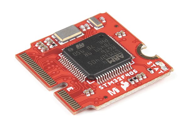
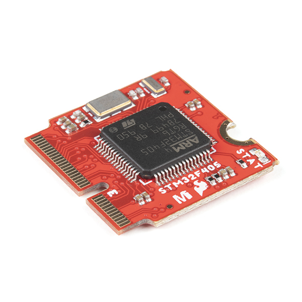
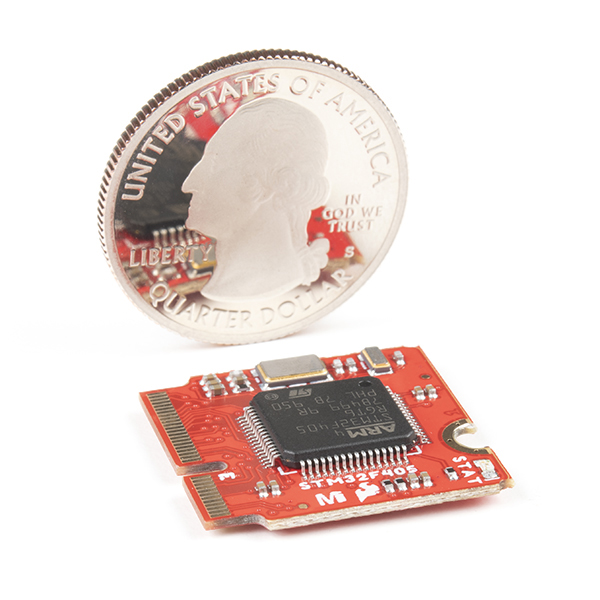
All of these reasons put together was why fabless semiconductor manufacturer, Quicklogic, developed the EOS S3 ultra-low-power multicore MCU which featured best-in-class audio front-end and powers Quicklogic’s Quickfeather platform, which was developed to make building voice-based embedded solutions easier.

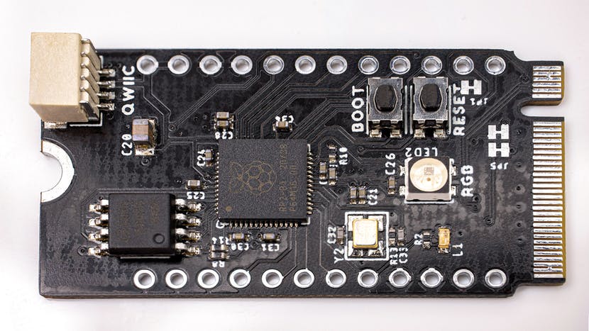
Based on (and compatible with) Adafruit’s open-source Feather Board, the Quickfeather was designed to enable the next generation of low-power Machine Learning (ML) capable IoT devices, and this combined with the QuickLogic’s Open Reconfigurable Computing (QORC) Initiative, and the EOS™ S3 Voice Processor, could be used to create superior user experience and long battery life voice-based system.

To shorten time to market for designers using the platform and make leveraging the potentials in these combinations easier, Quicklogics recently released the QuickFeather Alexa Close-Talk Reference design; created for Voice-Initiated, Hands-Free, Alexa Built-In Devices with Close-Talk Support.

According to Quicklogics,

“This is the first available always-listening, Close-Talk qualified smart hearable reference design based on QuickLogic’s ultra-low-power Arm® Cortex®- M4 Microcontroller”

and it can be used by designers and manufacturers to “evaluate the “Alexa” Built-In Close-Talk experience, optimized for battery-powered products” and build Proofs-of-Concept.

The EOS S3 integrates Sensory’s Low Power Sound Detection (LPSD) technology and runs DSP Concepts’ TalkTo noise suppression and beamforming technology that helps create an intuitive voice-based system, but beyond the reference design also shows how can integrate motion, and other Artificial Intelligence (AI) and Machine Learning (ML) use cases based SensiML’s AI Software Platform that already supports QuickLogic’s QuickFeather development kit.

Some highlight features of the Reference Design include:

  • Alexa Wake Word Engine (WWE) running in the EOS S3 voice processor
  • Hardware-optimized Low Power Sound Detection (LPSD) technology from Sensory™
  • Support for one or two microphone use cases with DSP Concepts’ TalkTo noise suppression and beam forming technology
  • Connectivity to Alexa Voice Service via Wi-Fi
  • Built on top of 100% open-source hardware QuickFeather dev kit and QORC open-source software tools
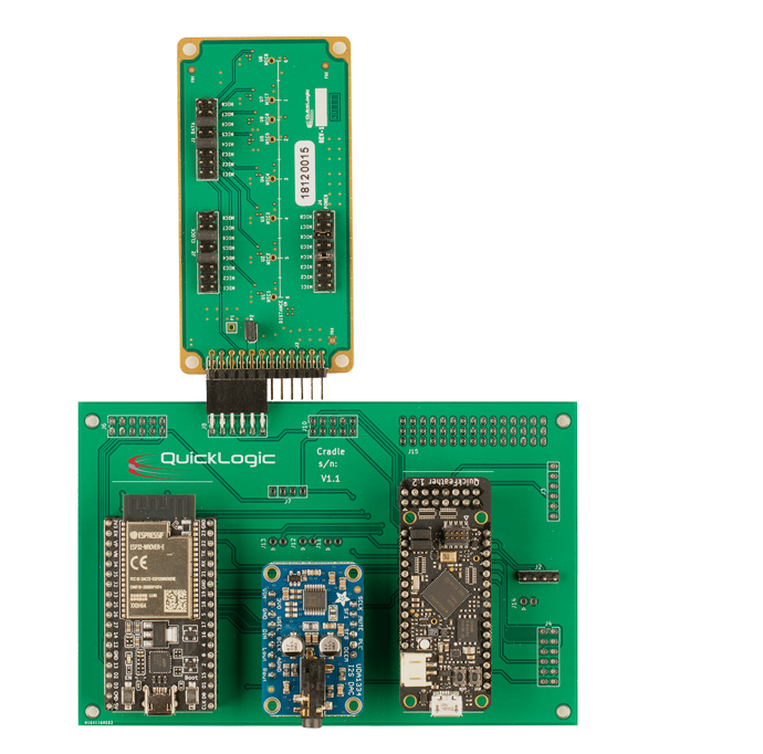
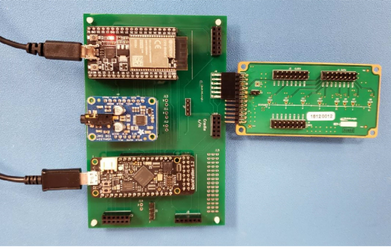
  • Comes with a QuickLogic QuickFeather Development Kit including the EOS S3 Low Power Voice Processor – Supported by 100% Open Source Hardware Development Kit and Software Tools
  • Espressif ESP32-WROVER-E WiFi Development Kit for WiFi connectivity
  • Adafruit I2S Audio Decoder for supporting playback from Alexa Voice Service directly to a standalone speaker
  • QuickLogic microphone daughtercard that supports variable microphone spacing
  • QuickLogic sturdy PCB cradle to reliably connect all components together

The reference design board is available for sale on the Quicklogics website for $149.

More information on the features of the board and its purchase, along with a manual showing how to use it can be found on the products page on Quicklogic’s Website.

RP2040 M.2 Card with M.2 Connectivity Form Factor

RP2040 M.2 card

There has been a lot of discussion about the Raspberry Pi’s RP2040 SoC in the past few months after the release of the Raspberry Pi Pico. The RP2040 SoC is also popular for its high-frequency clock covering a large range of applications at a very low cost. Timonsku a hardware designer has come up with a design for the M.2 interfacing of the SoC. This allows the miniaturization of the hardware at low power requirements. The edge connector of the design has a size of M.2 B key.

Timonsku’s design is an RP2040 M.2 card consisting of an RP2040 SoC, a WS2812 intelligent control LED, and a Qwiic connector. WS2812, an intelligent control LED light source in which the control circuit and RGB chip are combined in a package of 5050 components. It is a “simple, scalable and affordable full-color LED”. The board also comes with external GPIO pins allowing the input for the program from outside the CPU or providing the output to the user. The board also has reset and boot buttons on it.

Twitter Thread of RP2040 M.2 Card

Additionally, M.2 form factor is popular in SSDs. It is also called the Next Generation Form Factor (NGFF) due to its internal mounting capacity. This allows compatibility with the computer expansion cards and similar connectors. It is a good alternative to the mSATA standard, which uses the “PCI Express Mini Card physical card layout and connectors”.

There has been a discussion on the interfacing of the board with Desktops or Laptops as they come with M.2 slots. However, according to Timonsku, the M.2 slot of the RP2040 M.2 card may not be used with USB signals. As the M.2 specification does not compulsorily require them. Also, it would be difficult to automate the board while it is present on the laptop or computer. Hence, GPIO-level access would be necessary to work on the boot and reset signals.

Piunora Carrier Board

The Twitter thread of Timonsku shows the compatibility of the RP2040 M.2 card with the Piunora carrier board. This carrier board is also compatible with the popular Raspberry Pi CM 4 and transits it to Arduino R3 like form factor. Piunora carrier board has completed its goal of funding on the Crowd Supply at this point time.

The RP2040 M.2 card is still in the design phase and it is probable that the design would be soon open-source. For more information and updates on the card, you can keep checking Timonsku’s Twitter thread.

via Hackster

Electromagnetic near-field PCB Probes are open source

In modern compact electronic circuits, there are several components on a confined PCB area, and so, the electromagnetic effects induced from one component may affect the surrounding components. This disturbance is known as Electromagnetic Interference (EMI). The source of the radiation must be identified in PCBs to predict the EMC of electronic circuits. Electromagnetic compatibility (EMC) is the ability of electrical equipment and systems to function acceptably in their electromagnetic environment, by limiting the unintentional generation, propagation, and reception of electromagnetic energy which may cause unwanted effects such as EMI. Near-field scanning is the general method for identifying radiation sources in PCBs.

Electromagnetic near-field scanning

Near-field scanning is used for estimating localized electromagnetic emissions. The far-field is a region in which the field acts as normal electromagnetic radiation. But in the near-field region, electric and magnetic fields can exist independently. Additionally, in the near-field region, one type of field can dominate the other. E-field and H-field probes are used for electromagnetic near-field scanning. E-field probe measures point-to-point the electric field strengths locally. On the other hand, the H-field probe measures the magnetic field strengths locally.

E-field and H-field probes: An overview

The E-field probe consists of a short dipole antenna, a detector diode, a non-perturbing transmission line, and a readout device. Three orthogonal dipoles are generally used in an E -field probe to provide a response that is nearly isotropic for all polarizations of the incident field. Optical fibers, together with a suitably modulated light source, may be used to form a wide-band non-perturbing data link from the dipole and detector to a remote readout [1].

The H-field probe consists of a printed circuit magnetic loop and a transmission line. The magnetic flux from the loop will induce a high-frequency waveform that travels through a transmission line to the receiver. The transmission line is mostly a microstrip line.

Source: https://charleslabs.fr/en/project-Electromagnetic+interference+mapping

Implementing near field E-field and H-field probes on a printed circuit board is difficult mainly because it involves designing and implementation of non-perturbing transmission lines.

The below shown near-field probes are designed by Ketan Desai. He is a student of Electrical Engineering at the University of British Columbia.

The complete project including Gerber files can be found at: https://github.com/ketszim97/NearField_PCB_Probes#readme

Reference:

[1] H. Bassen and G. Smith, “Electric field probes–A review,” in IEEE Transactions on Antennas and Propagation, vol. 31, no. 5, pp. 710-718, September 1983, doi: 10.1109/TAP.1983.1143126.

JLCPCB & EasyEDA Finally Show UP Together

Design & Order on EasyEDA to Get $10 Voucher!

The Cheapest PCB prototype supplier and the first FREE online EDA tool show up together actually is not a piece of “new” news for many fans of JLCPCB or EasyEDA, but today i would like to give a brief introduction to those friends who did not know us. JLCPCB & EasyEDA,these two companies which sounds irrelevant while belong to the same group named JLC group.

Only $2, you can get 5 pcs PCB boards in JLCPCB

Make the PCB prototype much Easier and Cheaper.

JLCPCB is reputed as one of the most popular and powerful PCB Suppliers in china. Situated at the silicon of China, Shenzhen, JLCPCB has been in the PCB manufacturing and assembly industry for over 15 years, with assembly technologies of the highest quality standards, fastest delivery turnaround (as fast as 24hours), lowest manufacturer direct prices, and support via dedicated customer service. JLCPCB provide Free online price calculator,which make the PCB price automatically and transparently showed. And the Gerber Viewer give all the details of PCB design, helps much customers avoid the potential fault during manufacture.

EasyEDA, An Easier& Powerful Online PCB Design Tool

Make the Free EDA Tool into Reality

EasyEDA as a free, zero-install, Web and cloud-based EDA tool suite that integrates powerful schematic capture, hybrid mode circuit emulation, and PCB layout in a seamless cross-platform browser environment for electronics engineers, educators, students, and hobbyists.

As a totally free online EDA tool, EasyEDA has more than one million real-time updated components created on its parts library and users can create or import their own common libraries. And Benefit from China’s leading electronic components distributor – LCSC ,

EasyEDA supports direct links to more than 200,000 real-time, in-stock components at LCSC .

Designers can refer to stocks, prices, and order at any time during design.

The Combination of JLCPCB &EasyEDA

Makes the PCB &SMT Manufacture Easier

As far as we know,PCB prototype is an essential part of the development of any electronics product ,while the efficient EDA tool ensures reliable design.So the joint of JLCPCB the qualify PCB supplier and EasyEDA make the whole process from design to manufacture much more efficient than ever before.

From EasyEDA to JLCPCB, there is no need to generate the Gerber file into the manufacture system in JLCPCB. There is an interface where you can get your design directly manufactured through this button. There are few tips for how to place PCB or SMT orders directly from EasyEDA.

1 When you get PCB Design in EasyEDA; Use parts in JLCPCB Assembled library to design PCB, make better decisions with real-time visibility into parts availability and pricing. Confirm parts selection with confidence.

2 One click to order at JLCPCB;Once finishing your PCB design, click “Generate PCB Fabrication File(Gerber)” to preview your board, then order your design at JLCPCB with one click, and the Gerber files will be automatically uploaded on JLCPCB. Get $10 Voucher Now!

3 Simply generate the BOM and Pick&place files from EasyEDA, and upload them directly into our platform. Our system is compatible with EasyEDA formats.

4 Parts Confirmation; Since you’ve used parts from JLCPCB library, our system identifies all parts your need directly from the BOM and all parts can be confirmed automatically.

5 Quote & Order;Review the parts placement and check the component orientation, to know how we will assemble your board and see the instant price for SMT assembly service.

6 Order Delivering; Track the production process in real-time, and receive professionally assembled PCBs in One Week.

The Joint Activity of JLCPCB&EasyEDA is in Process

Get $10 off for your PCB +SMT Order Now!

New EDC Series Supercapacitors Offer Capacitance Values from 0.047 to 1.5 Farad

High Power Density, Coin Cell Supercapacitors from Cornell Dubilier in Stock at TTI

TTI, Inc., a leading specialty distributor of electronic components, has stock for immediate shipment of multiple values of the Type EDC series Stacked Coin Cell Package Supercapacitors from Cornell Dubilier (CDE).

The EDC series offers capacitance values from 0.047 to 1.5 Farad with voltages from 5.5VDC up to 6.3VDC. Supercapacitors can replace or extend battery life in onboard memory backup. With quick-response and recharge times, these supercapacitors offer higher power than batteries and greater energy than typical aluminum electrolytic capacitors without degradation over millions of charge-discharge cycles.

Three different case configurations are available including horizontal, vertical and radial-lead PCB mounting. The operating temperature for the EDC series is -25°C to +70°C. Applications include real-time clock (RTC) backup, power failure backup and battery assist.

To learn more, visit CDE Type EDC Coin Cell Supercapacitors at TTI.

MicroMod STM32 Processor improves MicroMod applications

SparkFun’s processor board improves MicroMod applications with its Arm® Cortex®-M4 32-bit RISC core

The SparkFun MicroMod STM32 processor board improves MicroMod applications with its Arm Cortex-M4 32-bit RISC core. This little processor board provides an economical and easy-to-use development platform for situations that require more power with minimal working space. With the M.2 MicroMod connector, connecting the STM32 processor is a breeze. Simply match up the key on the processor’s beveled edge connector to the key on the M.2 connector and secure it with a screw (included with all carrier boards). The STM32 is one of the most powerful and economical microcontrollers available, so to be able to add it to MicroMod carrier boards is a huge advantage for any project.

The STM32F405 processor is based on the high-performance Arm Cortex-M4 32-bit RISC core and can operate at a frequency of up to 168 MHz. This core features a floating point unit (FPU) single precision that supports all Arm single-precision data-processing instructions and data types. It also implements a full set of DSP instructions and a memory protection unit (MPU), which enhances application security. This processor board utilizes the DFU bootloader for uploading code and incorporates an extensive range of enhanced I/Os and peripherals. To complement the STM32F405 processor, SparkFun has also added an additional 128 Mb (16 MB) serial Flash memory chip to the underside of the board.

Features

  • Arm 32-bit Cortex-M4 CPU with FPU
    • Adaptive real-time accelerator (ART Accelerator™) allowing 0-wait state execution from Flash memory
    • Frequency up to 168 MHz
    • Memory protection unit
    • 210 DMIPS / 1.25 DMIPS/MHz (Dhrystone 2.1)
    • DSP instructions
  • 1 Mbyte of Flash memory
  • 192 Kbytes of SRAM including 64 Kbytes of core coupled memory (CCM) data RAM
  • Flexible static memory controller supporting compact Flash, SRAM, PSRAM, NOR, and NAND memories
  • Clock, reset, and supply management
    • 1.8 V to 3.6 V application supply and I/Os
    • 32 kHz oscillator for RTC with calibration
    • Internal 32 kHz RC with calibration
  • Low-power operation
    • Sleep, stop, and standby modes
    • VBAT supply for RTC, 20×32 bit backup registers + optional 4 KB backup SRAM
  • Debug mode
    • Serial wire debug (SWD) and JTAG interfaces
    • Cortex-M4 Embedded Trace Macrocell™
  • Advanced connectivity
    • USB 2.0 full-speed device/host/OTG controller with on-chip PHY
    • USB 2.0 high-speed/full-speed device/host/OTG controller with dedicated DMA, on-chip full-speed PHY and ULPI
    • 10/100 Ethernet MAC with dedicated DMA: supports IEEE 1588v2 hardware, MII/RMII

more information: https://www.sparkfun.com/products/17713

Meet the MeLE Quieter2; An Ultra-Thin, Ultra-Quiet, Fanless Mini PC

Guangdong-based electronics manufacturer, MeLe has been in the news a couple of times over the years for a number of their tiny but powerful intel mini processors-based desktop PCs. The company recently shared the beginning of sales of one of their latest creations; the MeLe Quieter 2, a fanless, small-sized PC based on an Intel Celeron J4125 processor.

Built on its proprietary passive cooling technology perfected in previous mini-PCs like the MeLe USB Stick, the Quieter, even with intensive computations, runs at 0dB silence, with no fan, and no vibration making it the best in class for application where smooth and quiet operations are a priority.

Featuring the Intel Celeron J4125 processor, the quieter2 brings the 2.0~2.7 GHz processing speed of the quadcore processor along with the Intel UHD Graphics 600, an 8GB LPDDR4 RAM, and a 128GB/256GB onboard storage (with support for up to 3TB Extension), all wrapped in a 131 x 81 x 18.3mm palm-sized rugged enclosure, giving it a size, cost, and power combo that’s one of the rarest in the league of minicomputers.

The Quieter2 was designed for use in applications ranging from home and office use to industrial applications and standalone systems like digital signage and IoT solutions. To make it effective for this broad range of applications, the Quieter2 comes with a good number of amazing features like the Kensington Lock Slot for security, and its support for Wake on LAN / PXE /BIOS One-Step Reset/ Auto Power on / RTC wake up, which provides the ideal solution for both home entertainment and commercial usage.

For connectivity, the Quieter2 features a 2.4G/5G dual-band Wi-Fi module, with a Gigabit LAN port which provides 1000Mbps fast and stable data transmission speed, and Bluetooth 4.2 through which users can connect with wireless peripherals like keyboard and mouse.

The Quieter comes with two HDMI ports both of which support 4K video outputs at 60Hz, with a maximum resolution of 4096×2160 that can transform any TV into an eye-catching digital signage screen and open up a world of computing possibilities to your home, office, or anywhere else you need it.

While it supports Linux and Ubuntu-based operating systems, the Quieter2 also supports windows and comes preloaded with a full version of Windows 10 Pro.

Highlight features and specification of the quieter2 are provided in the list below;

  • Intel Celeron Quad Core Processor: J4125 (2.0~2.7 GHz)
  • Intel UHD Graphics 600
  • Operating System: Pre-installed Windows 10 Pro (64-bit) ; Support Linux, Ubuntu
  • Language: pre-installed English, Spanish, Russian, French, German, Italian, Portuguese, Polish, Dutch, Swedish, Japanese, Korean, Arabic, Hebrew, etc.; Support 100+ languages
  • BIOS: Support Wake on LAN / PXE/ BIOS One-Step Reset/ Auto Power on/ RTC wake up
  • Memory: 8GB LPDDR4
  • Storage: 128GB/256GB on-board Storage
  • Storage expansion: Support Mirco SD card, M.2 SATA 2280 x1 / M.2 NVMe 2280 x1,
  • 4x USB 3.0
  • 2x HDMI 2.0 port
  • support 4K@60Hz
  • 1x 3.5mm Audio combo jack
  • 1x Micro-SD Card Slot
  • 1x Gigabit LAN Port
  • 1x Kensington Lock Slot
  • 1x USB Type-C (Only for power input: 12V2A)
  • 802.11a/b/g/n/ac Dual Band Wi-Fi (2.4Ghz/5.8Ghz)
  • Bluetooth 4.2
  • 1x Gigabit LAN Port
  • 131 x 81 x 18.3mm
  • Weight 203g

The Quieter2 is currently available for sale on MeLe Store on Alibaba for $246 with modifications to the basic offering that can take cost up to $258.

The package comes with a 1x Mini PC 1x Power Supply with EU/US/UK/AU Type Adapter (Adapters are optional depend on the sales regions) 1x Silicone cooling pad for SSD heat dissipation, and 1x User Manual.

When bought through their store, MeLe offers a 12-month warranty for the hardware of each product under normal usage excluding deliberate damage, accidents, misuse of the product, or damage caused by repairs or upgrades.

More information on the Mini PC and MeLe’s Offerings is available on the product page on Aliexpress.

Researchers develop MEMS vibrational energy harvesters for IoT Systems

IoT systems are very well known these days as they allow connection and exchange of data through the internet. The Internet of Things (IoT) systems consist of a network of sensors, actuators, software, and other technologies connected. Due to increasing design specifications and the need for compactness, dependence on energy sources like solar is not feasible. We need compact solutions which can deliver enough power to our IoT circuits. IoT wireless sensors consume a peak power of around tens of milliwatt. But if we schedule the transmission and reception in some intervals, we can bring it in the order of a few hundred microwatts.

Microelectromechanical systems (MEMS) is the most suitable technology to realize IoT-sensing nodes because it enables integrated fabrication of sensors/actuators, electronic circuits for information processing and radio frequency communication, antennas, and energy harvesters on a single chip or in a package. Low power transmitter and receiver networks with onboard MEMs energy harvesting systems can independently generate power for themselves. In this way, the level of connection can be further developed without having to worry about power requirements. MEMS refers to Microelectromechanical systems. It is a technology that consists of micro-electro-mechanical devices and structures that are made using microfabrication. MEMS energy harvesting means taking advantage of vibrations and other mechanical effects and converting them into electrical power.

Hiroshi Toshiyoshi from the University of Tokyo and his colleagues recently published their study on MEMS vibrational energy harvesters. In this paper, researchers look into the fundamental mechanism to retrieve the power from physical vibrations by using microelectromechanical systems (MEMS) energy harvesters. They discuss the deliverable power they recorded and the mechano-electric power conversion techniques like electrostatic induction, electromagnetic induction, and piezoelectric effect.

Vibrational Energy Harvester

The vibrational energy harvesting method takes advantage of the mechanical energy present in the surroundings. The surrounding mechanical vibrations in the environment have a particular dominant frequency. When we tune an electrical oscillator (which is fabricated on-board) at this dominant frequency, we can expect to see power generated. This concept is similar to the impedance-matching concept in which for maximum power transfer, we match the load with the output resistance of the circuit. Such a mechanism is usually referred to as the velocity-damped resonance generator (VDRG), as the velocity of a physically exciting mass is mechano-electrically coupled to deliver electrical power to the external load.

This phenomenon is explained in the study with the help of a two-mass model. Here an inertial mass m is suspended with spring constant k and cin represents the inertial loss. In our circuit, the Cin represents the internal loss that consumes power within the energy harvester. The power that can be harvested is denoted by Cex.

Now we turn our attention to harvester devices used to harvest the above-mentioned vibrational energy.

Electrostatic device:

Electrostatic device harvests energy from the so-called ‘electrets’ or permanent electrical charges. They can generate internal and external electric fields and are equivalent to a permanent magnet that can store electrical charges for a prolonged period (as long as 100 years). The researchers used silicon oxide as the electret material. Silicon oxide is known to be negatively charged when it contains potassium ions driven out by electrostatic force. Researchers used the silicon oxide on the surface of MEMS electrodes as an electret skin to induce electrostatic displacement current.

The electrostatic displacement current is generated when a conductor is doing a mechanical motion in the presence of electric fields. The below figure shows the electrostatic current generated by the comb-shaped electrodes.

Instead of electrodes, piezoelectric material can also be used for the generation of electricity. Piezoelectric generators built around Quartz crystal are very popular and they generate electrical energy when subjected to mechanical strain. Although thin-film piezoelectric materials are available for microfabrication, piezoelectric constants of these materials are typically lower than those of the bulk PZT.

Electromagnetic device:

The relative motion of permanent magnets and coils dictates the amount of electrical power generated. It follows from faraday’s law that the changes in magnetic field induce an electric field and thus, here the mechanical motion of permanent magnets and coils induces electric power. One of the unique features of the electromagnetic energy harvester is the flexibility in magnetic circuit design. Even the single-coil and a magnet pair can be operated in two different configurations depending on the direction of the relative displacement of the two components.

Thus, as this study focuses on on-chip electricity generation from surrounding vibrations, it will aid in the growth of advanced and more sophisticated IoT systems that will be developed in the future.

Full Article: https://www.tandfonline.com/doi/full/10.1080/14686996.2019.1569828

Buck converter PCB design replaces TO-220 regulators

Linear voltage regulators are used to maintaining a steady output voltage. They are step-down converters where the input voltage is always higher than the output voltage. The output voltage can be adjusted by external resistors. 78xx series is a very popular linear voltage regulator series. 78xx series, however, do not require external components for setting the output voltage. The regulators have some dropout voltage which can be defined as the input voltage minus the desired output voltage. It should be noted that if the desired output voltage is higher than Vin-Vdropout, then the linear regulator can’t regulate the output at the desired output voltage. In LM1117, the dropout voltage is around 1.25V which is very small compared to 78xx and so it is called a Low-Dropout (LDO) regulator.

Linear Voltage Regulator Design

Source: http://www.mosaic-industries.com/embedded-systems/microcontroller-projects/electronic-circuits/program-regulator-voltage

The voltage regulator ICs consists of a high-gain operational amplifier, a feedback network, and a pass transistor. The gate of the pass transistor is controlled by the output of the operational amplifier. The output voltage is sensed via a resistor divider network and is fed to the inverting pin of the OP-AMP. The sensed voltage is compared with the reference voltage and the high gain of the OP-AMP forces the reference voltage and the sensed voltage to be equal. In the 78xx series, the voltage divider ratio is fixed internally. On the other hand, in LM1117, the voltage divider ratio can be set via an external resistor. This gives the LM1117 IC flexibility in terms of output voltage.

Linear voltage regulators have a major issue. The input current required to the regulator is always the same as the output current. Additionally, the input voltage is always higher than the output voltage. Therefore, the input power is always higher than the output power. The difference is dissipated in the form of heat by the regulator. This means that the heatsink is necessary for many applications and sometimes, substantial power is wasted during regulation. To overcome these issues, buck converters can be preferred over linear regulators as they are more efficient and do not require heatsink.

Buck-converter design

Source: https://www.researchgate.net/figure/Circuit-Diagram-of-Buck-Converter_fig1_262632844

Buck-converter is a switching step-down converter. It consists of a switch (implemented by a MOSFET), energy storage elements like inductors and capacitors, and a diode. When the switch is open, in other words, when the MOSFET is not ON, the current in the circuit is zero. When the switch is closed, the current in the inductor begins to rise. The energy in the inductor is stored in the form of the magnetic field. When the switch is opened again, the inductor starts to discharge and powers the load. And, when we close the switch again while there is still energy left in the inductor, the output voltage is always greater than zero.

The output voltage depends on the input voltage and the duty cycle of the MOSFET. The relation between the input and voltage is given by Vout = D*Vin. If the duty cycle is 50%, then the output voltage would be half the input voltage.

Buck converter PCB 

Ketan Desai, a student at the University of British Columbia designed a buck converter PCB which can be used in replacement of 78xx and LM1117 voltage regulators. It is built around a very compact RPX-1.0 DC-DC converter IC which comes with an integrated inductor. The 78xx compatible version is as follows:

Source: https://github.com/ketszim97/TO_220_Buck/blob/78xx/TO_220_Buck.pdf

Below is the LM1117 compatible version. The only difference is in the pinout.

Source: https://github.com/ketszim97/TO_220_Buck/blob/LM1117/TO_220_Buck.pdf

Both the above designs are configured for 3.3V. Replacing R3 will allow the output voltage to be set.

Output Voltage R3 Value
1.5V 86k6
1.8V 60k4
2.5V 35k7
3.3V 24k3
5.0V 14k3
12V 5k36
24V 2k61

Complete project link: https://github.com/ketszim97/TO_220_Buck

RedRock TMR Low-Power Magnetic Switch Sensor

Coto Technology’s RedRock TMR ultra-low-power magnetic switch sensor features high sensitivity and miniature size

Coto Technology’s RedRock series of analog and digital TMR low-power magnetic switch sensors are ideally suited to the demands of next-generation security, metering, medical, automotive, instrumentation, industrial markets, and any application requiring a magnet and sensor. Due to their ultra-low-power (especially important in battery-powered applications), high sensitivity, miniature size, robustness, and availability, TMR sensors are a popular alternative to both Hall effect sensors and reed switches. Target applications include fluid level detection; door, window or lid open-close detection; water and gas meters; proximity sensing; rotary sensing; and any application where the device or product needs to wake up, turn on, and perform, thus providing a true out-of-the-box experience. These tiny sensors offer high magnetic sensitivity with high hysteresis, EMF resistance, and a small package size, all while consuming extremely low power.

Resources

Features

  • Low power consumption
  • High sensitivity
  • Stable temperature performance
  • Resistant to mechanical stress
  • Tiny size
  • Reach compliant
  • RoHS compliant

more information: https://www.cotorelay.com/product/redrock-rr111-series-tmr-analog-magnetic-sensor/

TOP PCB Companies