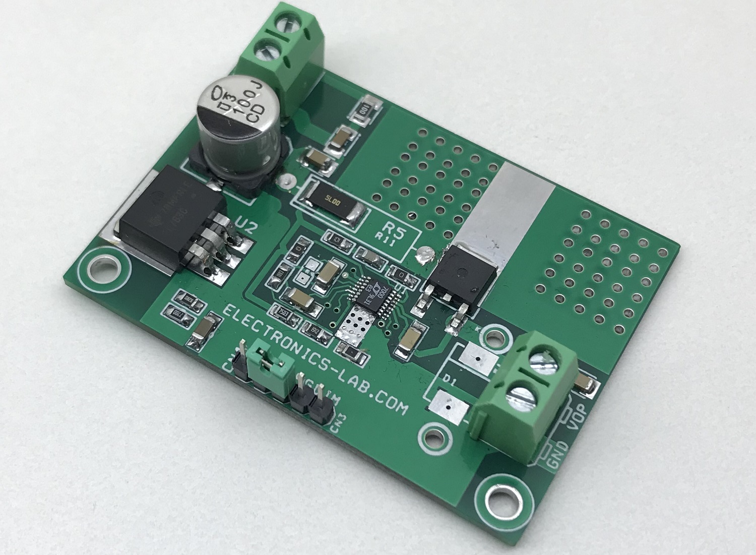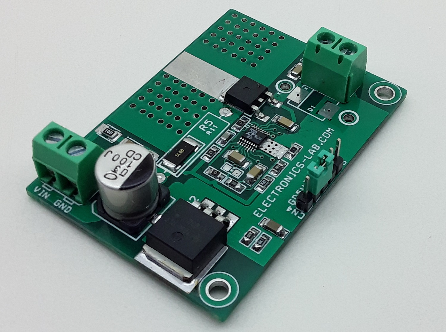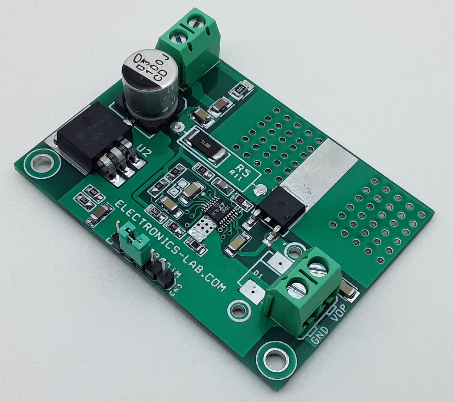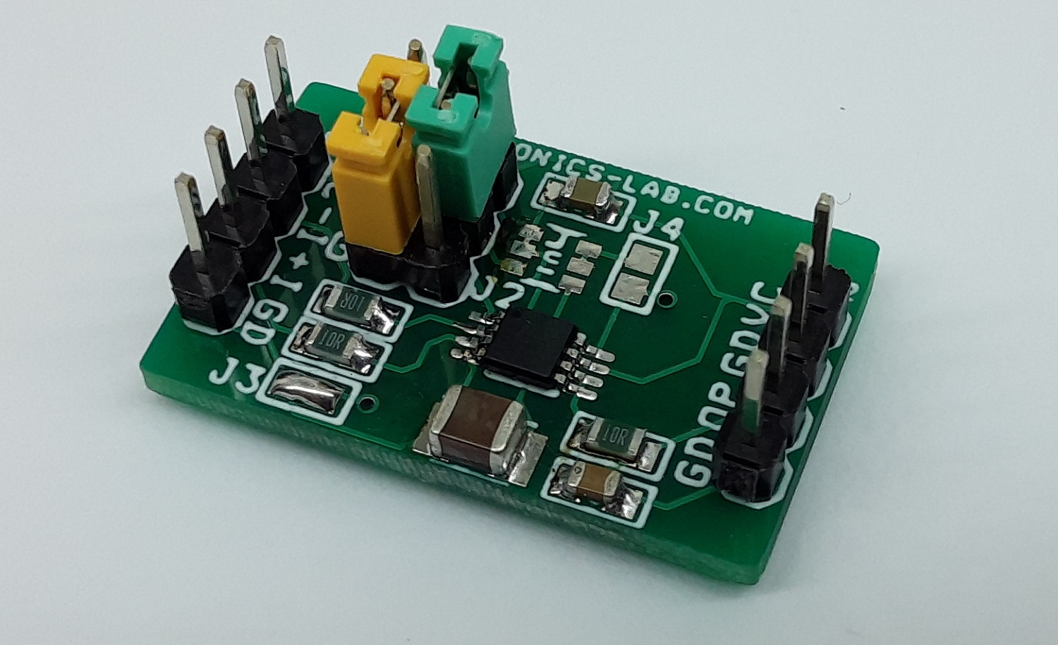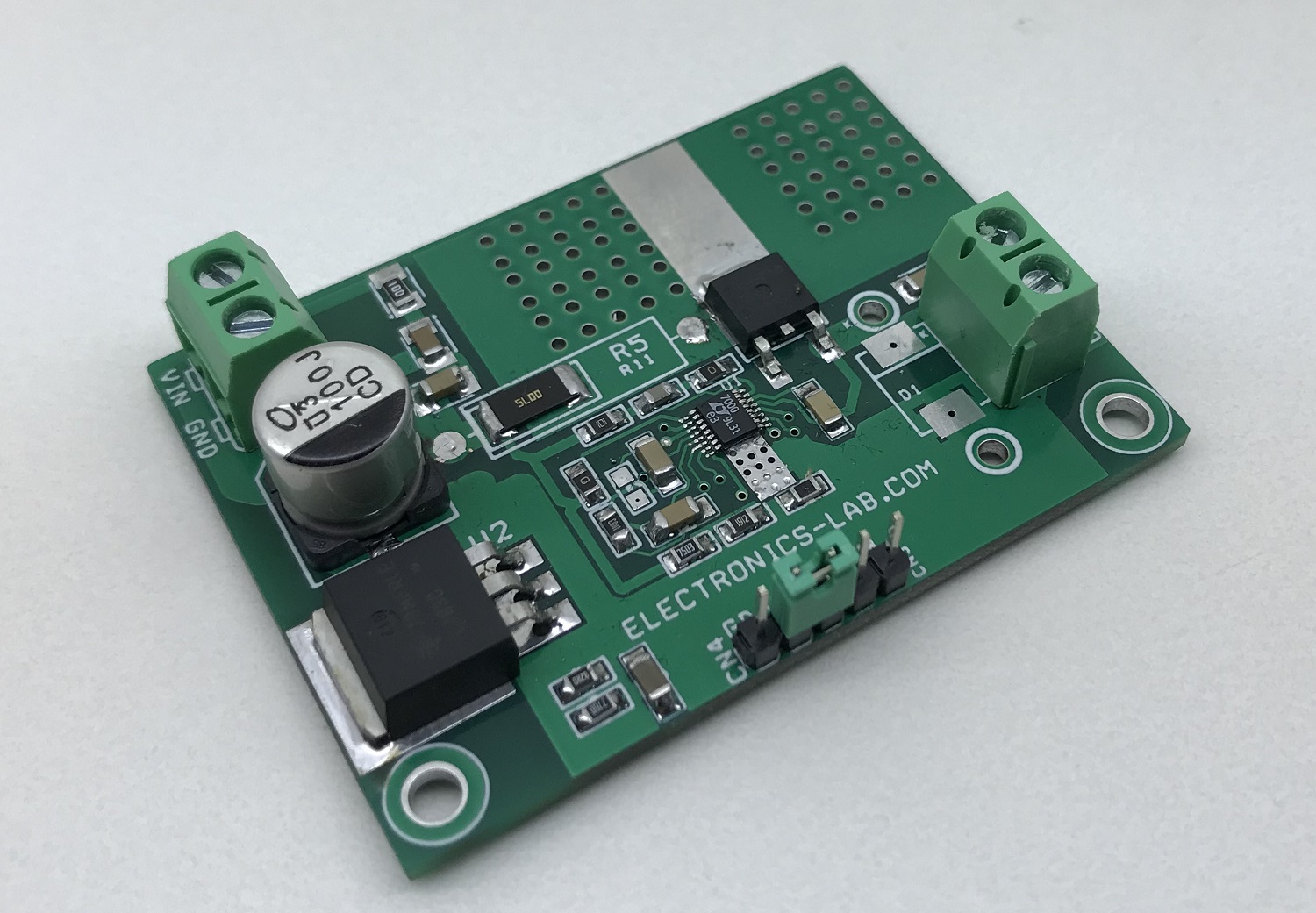
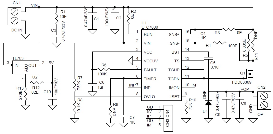
The project here is a 48V protected, high side switch designed to switch a 5A output load from input voltages from 8V to 48V. The circuit helps the user to easily ON/OFF the high current and voltage load with over-voltage lockout and over-current protection. The wide input range and low shutdown current (1μA typical) make it suitable for automotive, industrial, medical instruments, and telecom applications. This board offers a low 50ns (typical) propagation delay, fast switching times (<10ns), and 100% duty cycle operation. The project is based on LTC7000 which is a fast high voltage protected high side N-channel MOSFET driver. An internal charge pump fully enhances an external N-channel MOSFET switch, allowing it to remain on indefinitely. Its powerful gate driver can drive large gate capacitance MOSFETs with very short transition times, ideal for both high-frequency switching and static switch applications.
The circuit operates over an 8V to 48V input supply range. When an external current sense resistor and internal comparator sense that the switch current has exceeded a pre-set level, a fault flag is asserted and the switch is turned off after a period of time set by an external timing capacitor C7. After a cooldown period, it goes back on. The circuit is also configured to act when an overvoltage condition occurs. When voltage rise more than setpoint of 48V it switches off the output and remains off until input is cycled. Resistors R7, R8 are provided to set the overvoltage lockout, R10 sets the overcurrent limit, U2 5V is a regulator, Pin 3 (IMP) of CN3-CN4 provided to enable the output. This pin needs a High-level TTL-5V signal to enable the output, connect this pin to 5V to enable the output. When a fault condition occurs, disconnect the IMP pin from 5V and connect it to GND, pull up this pin to recycle the output.
Features
- Supply 8V to 48V DC
- Load Current 5Amps
- Over Voltage threshold 48V
- Easy On/OFF the high voltage and High Current Load
- Overvoltage Lockout
- Over Current Protection
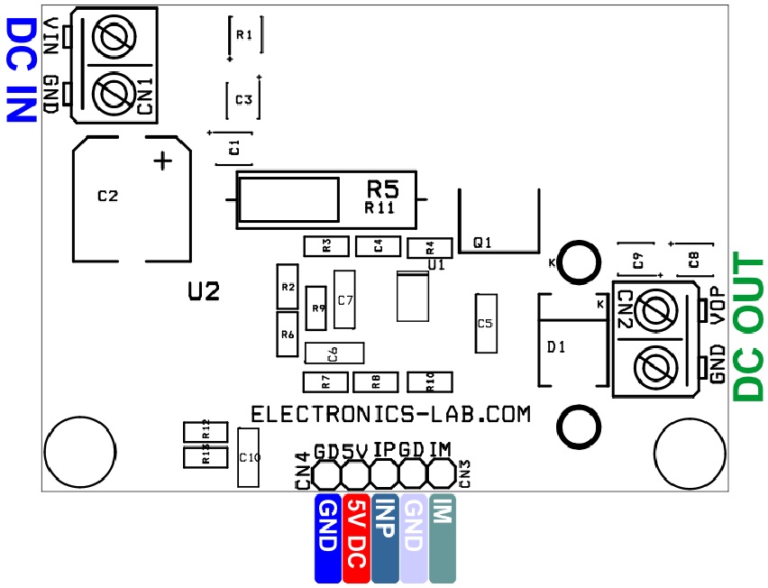
- PCB Dimensions 61.28 x 43.66 mm
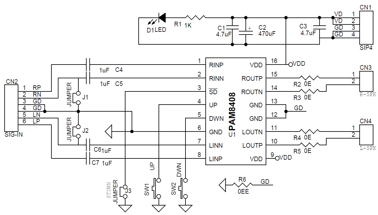
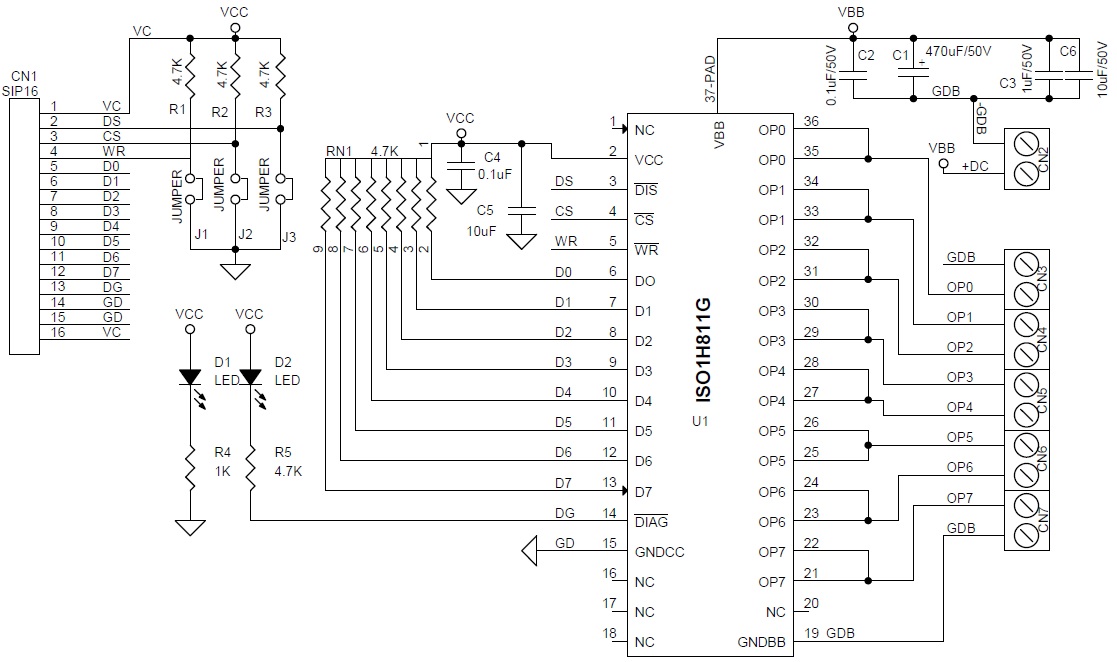
Schematic
Parts List
| NO. | QNTY. | REF. | DESC. | MANUFACTURER | SUPPLIER | SUPPLIER PART NO |
|---|---|---|---|---|---|---|
| 1 | 1 | CN1 | 2 PIN SCREW TERMINAL 5.08MM PITCH | PHOENIX | DIGIKEY | 277-1247-ND |
| 2 | 1 | CN2 | 2 PIN SCREW TERMINAL 5.08MM PITCH | PHOENIX | DIGIKEY | 277-1247-ND |
| 3 | 1 | CN3-CN4 | 5 PIN HEADER 2.54MM PITCH | WURTH | DIGIKEY | 732-5318-ND |
| 4 | 4 | C1,C3,C8,C9 | 0.47uF/63V SMD SIZE 1206 | MURATA/YAGEO | DIGIKEY | 399-C1206C474KMREC7210CT-ND |
| 5 | 1 | C2 | 100uF/63V ELECTROLYTIC | NICHICON | DIGIKEY | 493-6185-1-ND |
| 6 | 2 | C4,C7 | 1KPF/50V SMD SIZE 0805 | MURATA/YAGEO | DIGIKEY | |
| 7 | 1 | C5 | 0.1uF/50V SMD SIZE 0805 | MURATA/YAGEO | DIGIKEY | |
| 8 | 1 | C6 | 1uF/50V SMD SIZE 1206 | MURATA/YAGEO | DIGIKEY | |
| 9 | 3 | D1,R9,R11 | DNP | |||
| 10 | 1 | Q1 | FDD86369 | ON SEMI | DIGIKEY | FDD86369OSCT-ND |
| 11 | 1 | R1 | 10E 5% SMD SIZE 1206 | MURATA/YAGEO | DIGIKEY | |
| 12 | 2 | R2,R3 | 0E SMD SIZE 0805 | MURATA/YAGEO | DIGIKEY | |
| 13 | 1 | R4 | 100E 5% SMD SIZE 0805 | MURATA/YAGEO | DIGIKEY | |
| 14 | 1 | R5 | 0.005E 1% SMD SIZE 2512 | ROHM | DIGIKEY | RHM.005AUCT-ND |
| 15 | 1 | R6 | 100K 1% SMD SIZE 0805 | MURATA/YAGEO | DIGIKEY | |
| 16 | 1 | R7 | 750K 1% SMD SIZE 0805 | MURATA/YAGEO | DIGIKEY | |
| 17 | 1 | R8 | 19.1K 1% SMD SIZE 0805 | MURATA/YAGEO | DIGIKEY | |
| 18 | 1 | R10 | 75K 1% SMD SIZE 0805 | MURATA/YAGEO | DIGIKEY | |
| 19 | 1 | R12 | 82E 1% SMD SIZE 0805 | MURATA/YAGEO | DIGIKEY | |
| 20 | 1 | R13 | 270E 1% SMD SIZE 0805 | MURATA/YAGEO | DIGIKEY | |
| 21 | 1 | U1 | LTC7000 | ANALOG DEVICE | DIGIKEY | LTC7000IMSE#PBF-ND |
| 22 | 1 | U2 | LT783 | TI | DIGIKEY | 296-20778-1-ND |
| 23 | 1 | C10 | 10uF/10V SMD CAPACITOR SIZE 1206 | SAMSUNG | DIGIKEY | 1276-1137-1-ND |
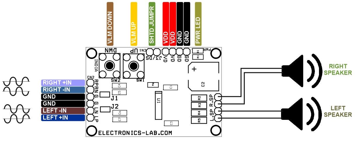
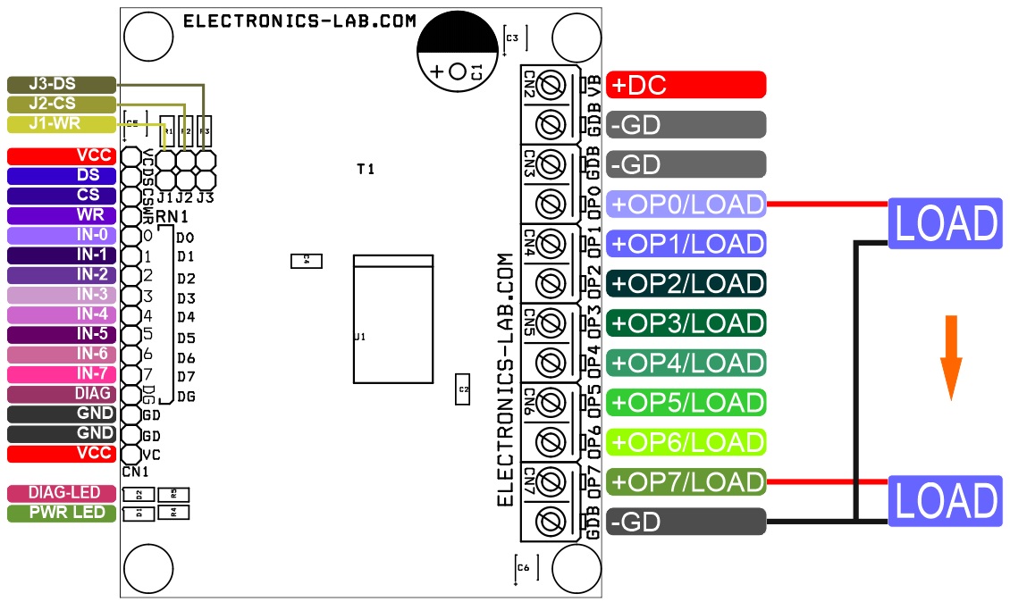
Connections
Gerber View
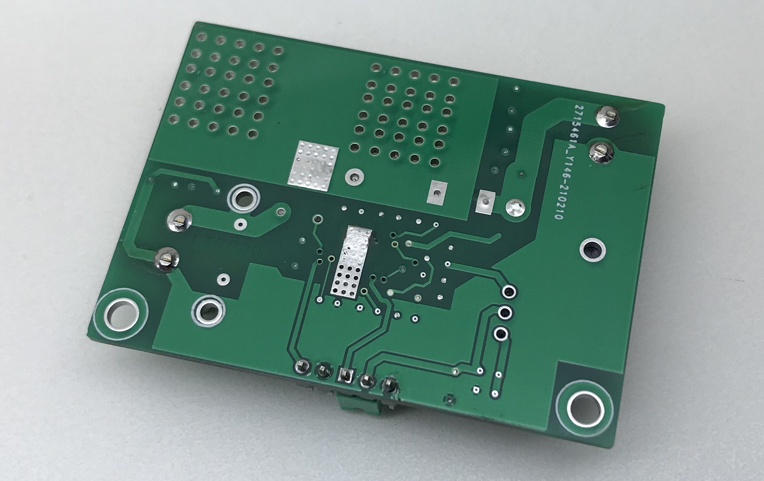
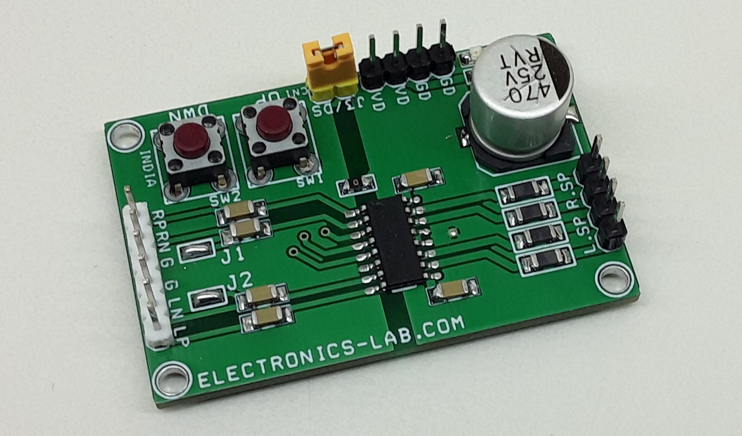
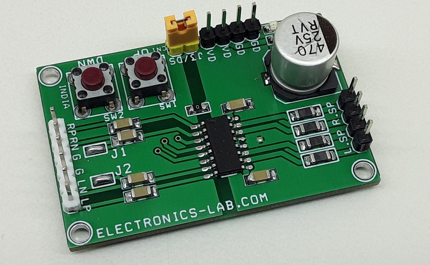
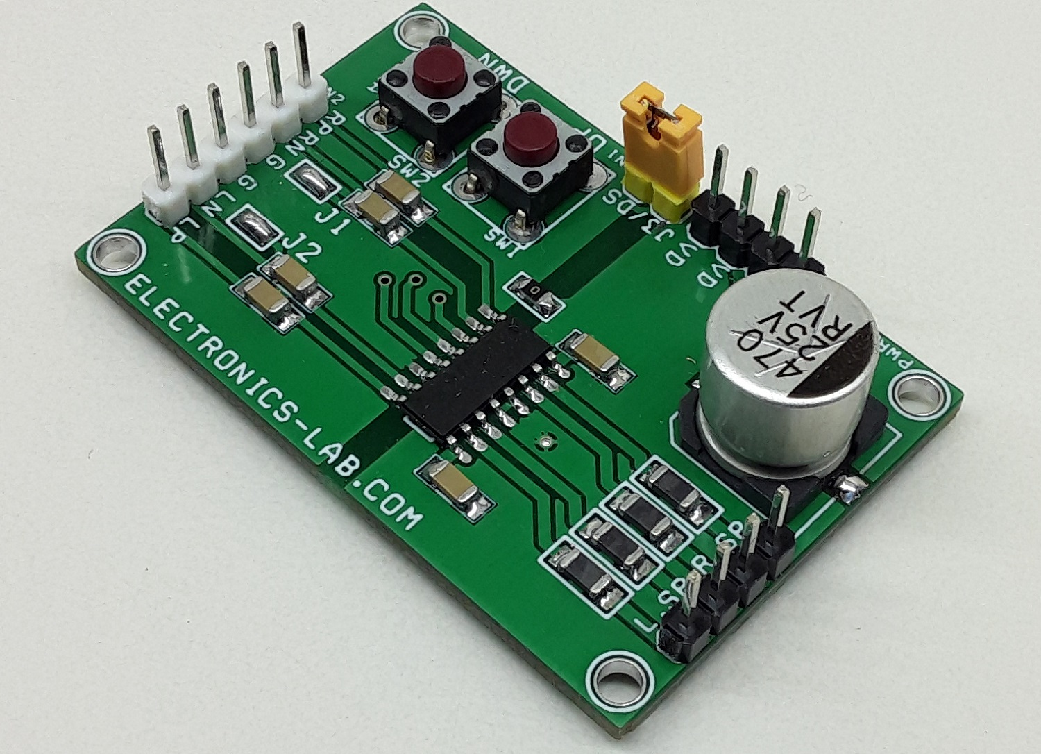
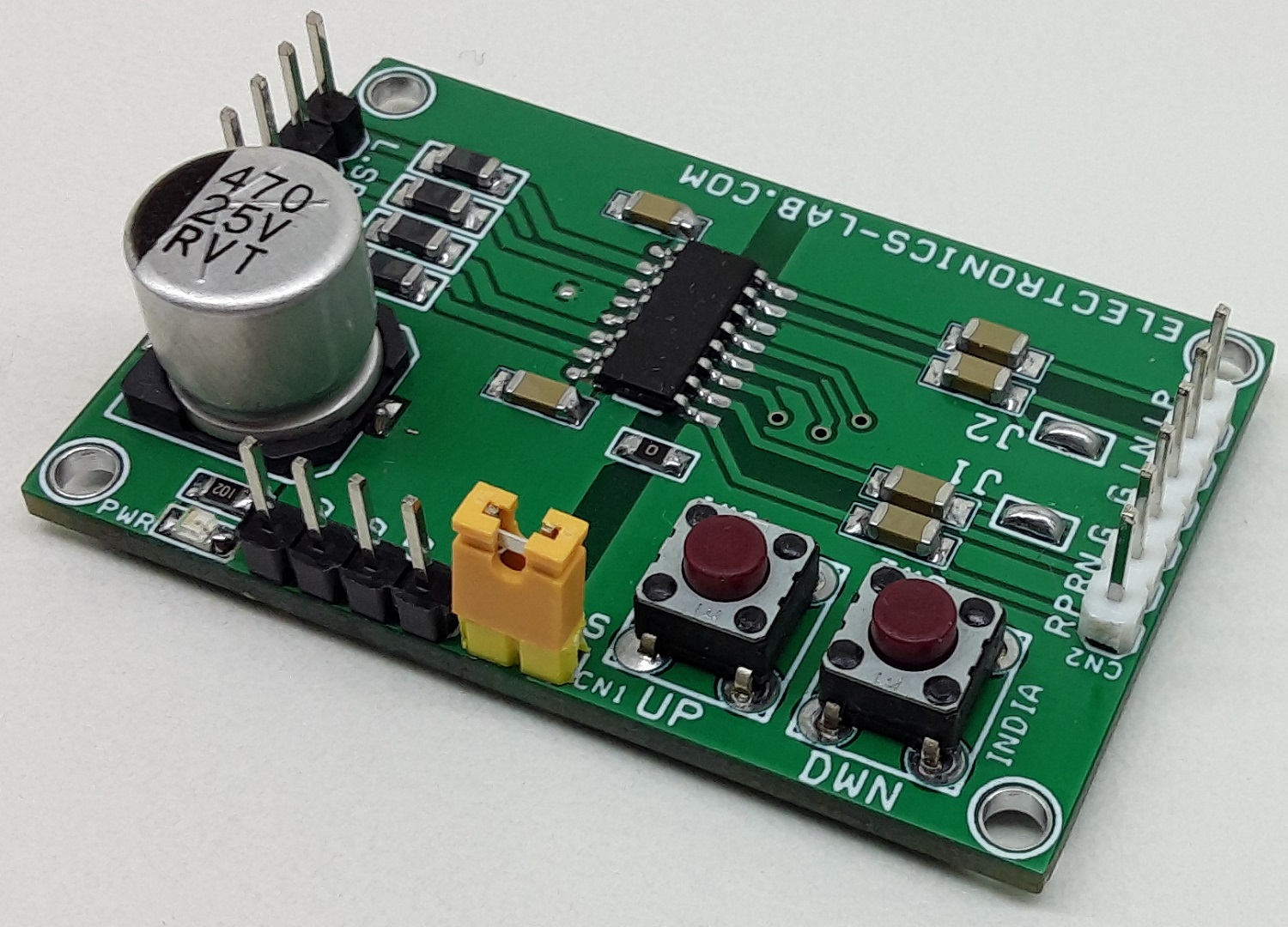
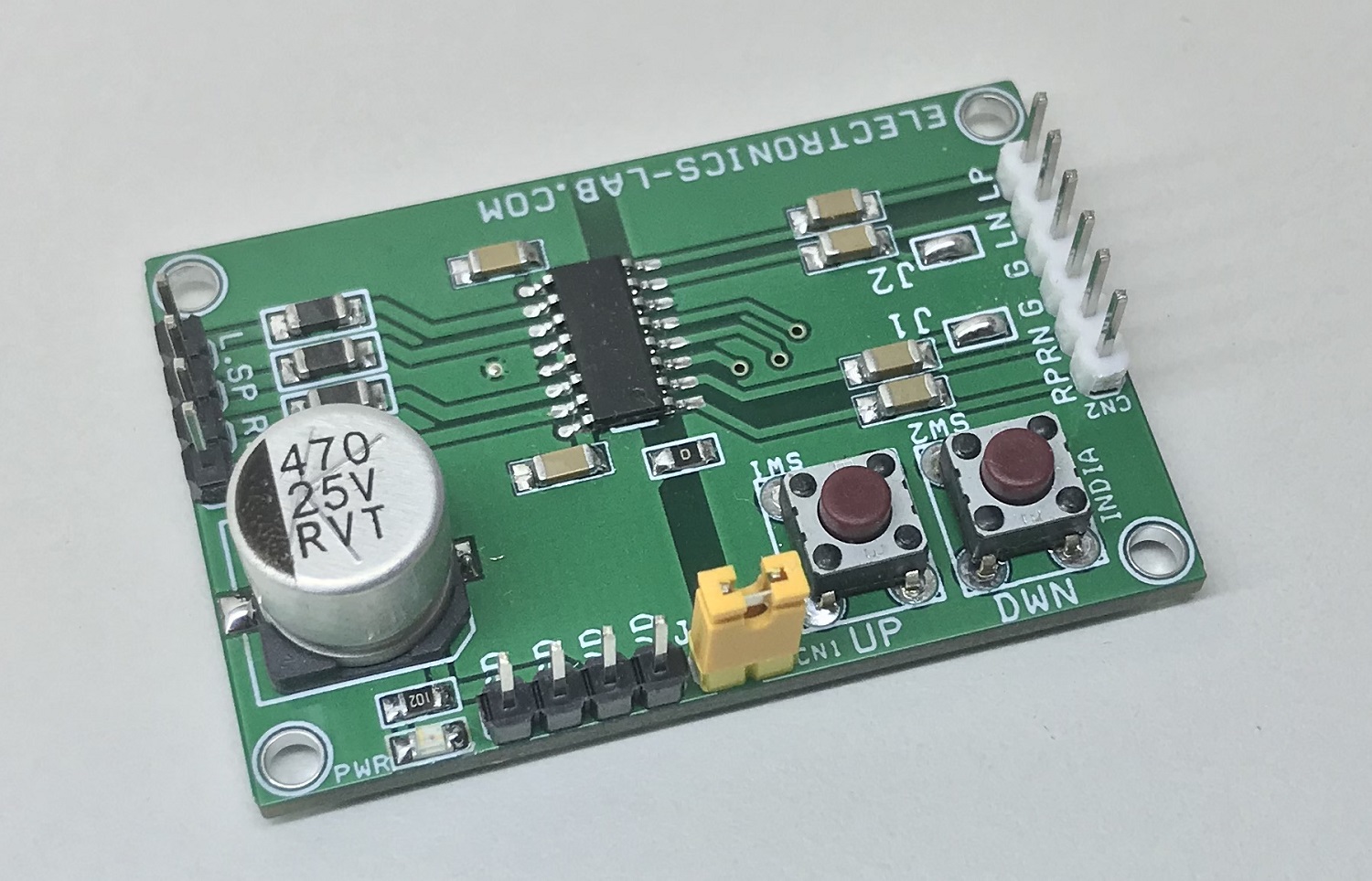
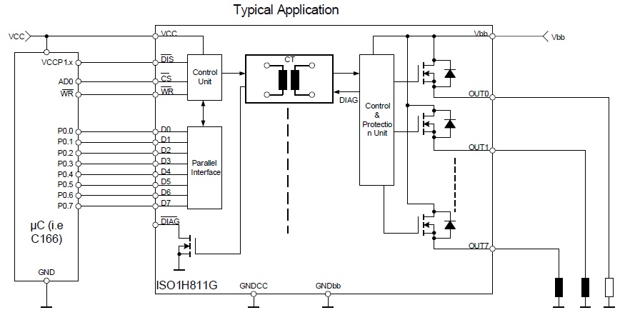
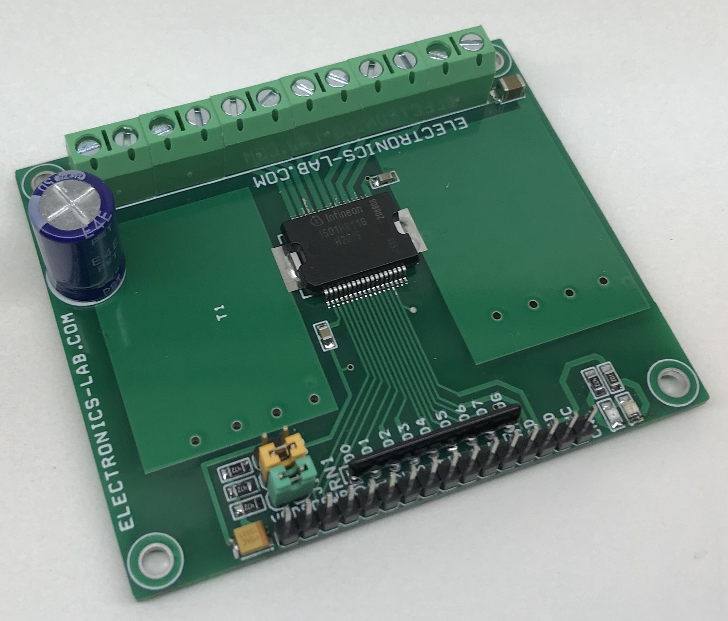
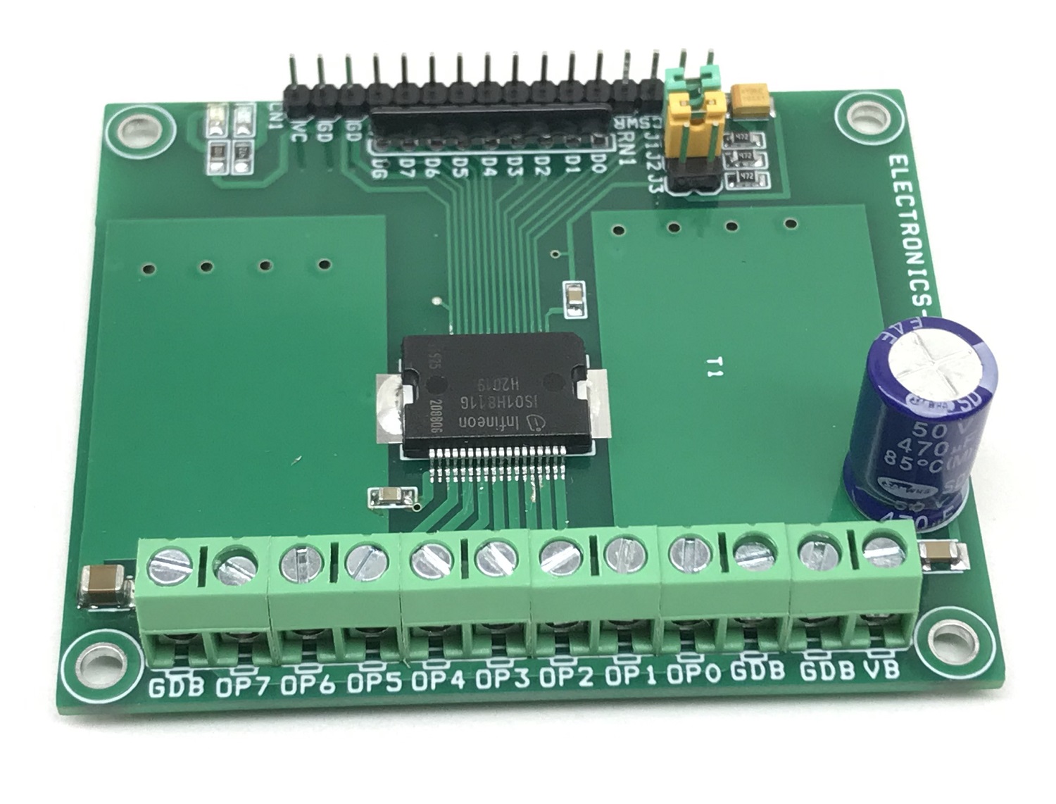
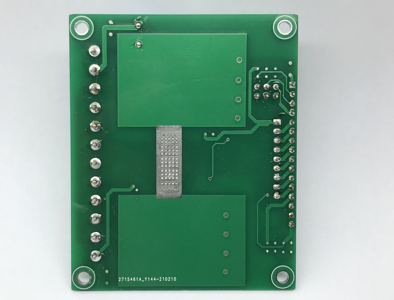
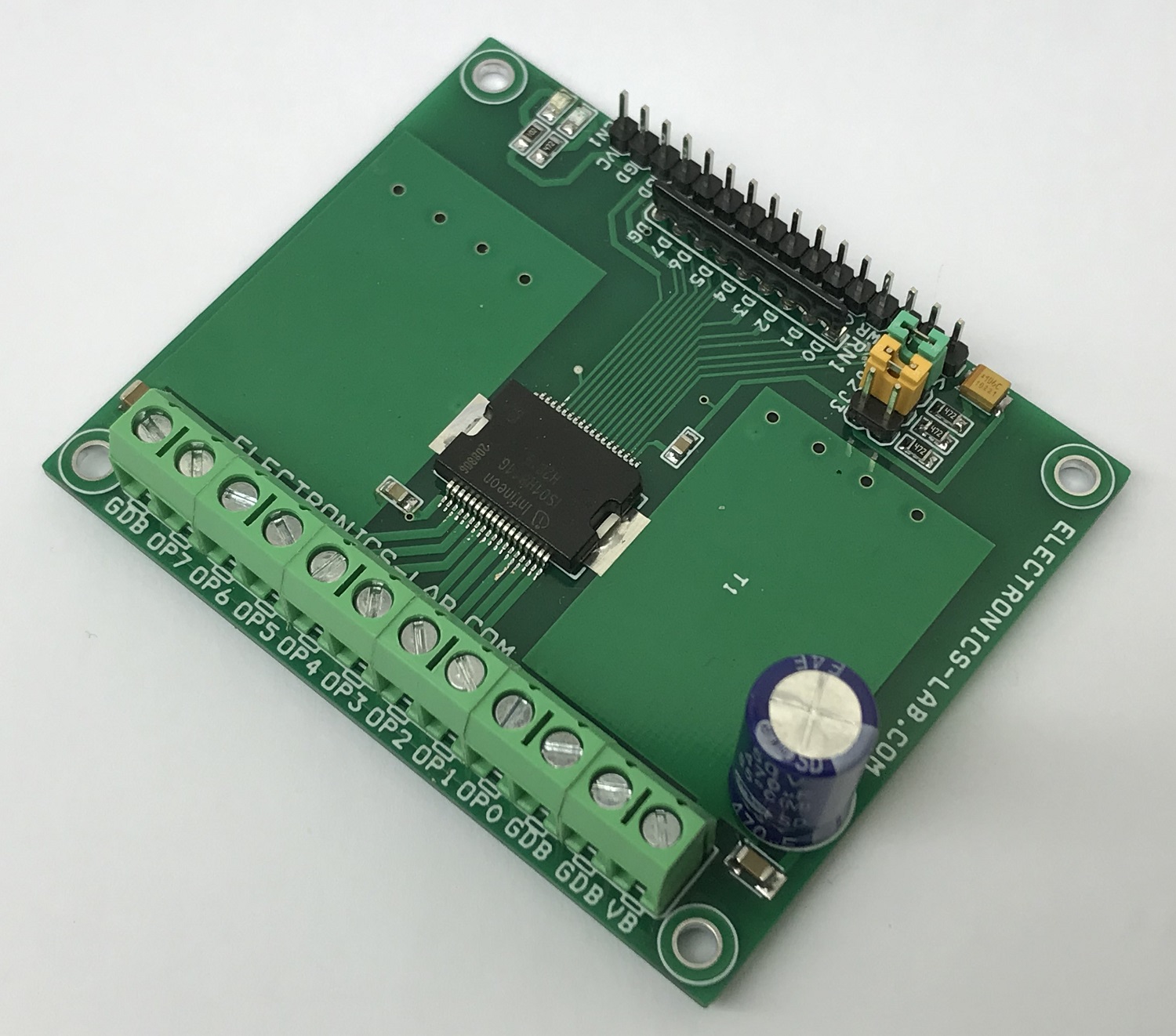
Photos