Switch debounce circuit uses only one gate

The circuit in Figure 1 produces a single debounced pulse each time you press S1. Moreover, the circuit uses only logic power from the remote pull-up resistor, R2. You can use the circuit to detect when a key is pressed in a non-energized device, such as a device in a system that’s just coming up from standby.

The circuit operates as follows: Assume that you have not yet pressed S1 and that C1 is in a charged state. Under these conditions, R1 drives IC1 toward VSS (ground), causing the IC to consume virtually no power. This action allows VOUT to remain near 5 V. However, when you press S1, C1 rapidly discharges and drives IC1 toward VDD. Under these circumstances, IC1 conducts heavily, pulling VOUT near 0 V until R1 charges C1 enough to again drive IC1 toward VSS. Once C1 charges sufficiently, IC1 goes to VSS and stops drawing power. This action unloads VDD and causes VOUT to return to a high state. D1 to D3, in conjunction with R3, shifts the level of VOUT for improved compatibility with CMOS logic.

[source: https://www.edn.com/switch-debouncer-uses-only-one-gate/]

AMS AG TMF8805 ToF 1D time-of-flight sensor

The TMF8805 is a time-of-flight (TOF) sensor in a single modular package with associated VCSEL

The TMF8805 is a time-of-flight (TOF) sensor in a single modular package with associated VCSEL. The TOF device is based on SPAD, TDC, and histogram technology. The device achieves a 2500 mm detection range.

Key features

  • Direct ToF technology with high sensitivity SPAD detection
  • 20…2500 mm distance sensing at 30 Hz
  • On-chip histogram processing
  • Industry’s smallest modular OLGA 2.2 x 3.6 x 1.0 mm package

Additional features

  • Fast Time-to-Digital Converter (TDC) architecture
  • Sub-nanosecond light pulse
  • 940nm VCSEL Class 1 Eye Safety
  • High-performance on-chip sunlight rejection filter and algorithm

Additional Benefits

  • Delivers high SNR, wide dynamic range, and no multi-path reflections
  • Enables dark and sunlight environment distance measurement within ±5%
  • Provides best-in-class resolution ranging mode detection sensing
  • Enables accurate distance measurements
  • Provides high accuracy, greater distance between cover glass, dynamic cover glass calibration, dirt or smudge removal and crosstalk compensation
  • Eye-safety circuitry stops VCSEL driver if VCSEL fault occurs
  • Optical filters with algorithm support enable high ambient light resilience
  • Reduce board space requirements, enables low-profile system designs in restricted space Industrial Designs

Internal Diagram

more information: https://ams.com/tmf8805

Texas Instruments TMUX6219 Single Channel 2:1 (SPDT) Switch

Texas Instruments TMUX6219 Single Channel 2:1 (SPDT) Switch is a complementary metal-oxide semiconductor (CMOS) switch in a single channel, 2:1 (SPDT) configuration. The device works with single supply (4.5V to 36V), dual supplies (±4.5V to ±18V), or asymmetric supplies (such as VDD = 8V, VSS = –12V). The TMUX6219 supports bidirectional analog and digital signals on the source (Sx) and drain (D) pins ranging from VSS to VDD.

The Texas Instruments TMUX6219 can be enabled or disabled by controlling the EN pin. When disabled, both signal path switches are off. When enabled, the SEL pin can be used to turn on signal path 1 (S1 to D) or signal path 2 (S2 to D). All logic control inputs support logic levels from 1.8V to VDD, ensuring both TTL and CMOS logic compatibility when operating in the valid supply voltage range. Fail-Safe Logic circuitry allows voltages on the control pins to be applied before the supply pin, protecting the device from potential damage.

The TMUX6219 is part of the precision switches and multiplexers family of devices. These devices have very low on and off leakage currents and low charge injection, allowing them to be used in high precision measurement applications.

Block Diagram

Features

  • ±4.5V to ±18V dual supply range
  • 4.5V to 36V single supply range
  • 2.1Ω low on-resistance
  • -10pC low charge injection
  • 330mA (maximum) high current support
  • –40°C to +125°C operating temperature
  • 1.8V logic compatible
  • Fail-safe logic
  • Rail-to-rail operation
  • Bidirectional signal path
  • Break-Before-Make switching

more information: https://www.ti.com/product/TMUX6219

Elektor Project: Wi-Fi for LoRa Switch

Clemens Valens @ Elektor Labs writes:

We published a remote-controlled switch in the March/April 2020 edition of Elektor magazine. It had state feedback and communicated using LoRa. Because it was housed in a waterproof IP66 enclosure, it was suitable for outdoor use. It was also a modular project with the relay and power circuitry on one board and the LoRa communication part on another.

This interested me, because I was looking for an outdoor switch that could be integrated easily into my home automation system. This system is based on Home Assistant and Wi-Fi, but not LoRa. I am sure it is possible to add LoRa to it, but I didn’t want to dive into that. Instead, I thought that by simply replacing the LoRa module with a Wi-Fi module, I could make it run ESPHome, which works great with Home Assistant (Figure 1).

Elektor Project: Wi-Fi for LoRa Switch – [Link]

Analog Devices Inc. ADPD188BI Integrated Optical Module

Analog Devices Inc. ADPD188BI Integrated Optical Module is a complete photometric system for smoke detection using optical dual wavelength technology. The module integrates a highly efficient photometric front end, two light emitting diodes (LEDs), and two photodiodes (PDs). The module is housed in a custom package to prevent light from going from the LED to the photodiode without entering the smoke detection chamber.

The front end of the application specific integrated circuit (ASIC) consists of a control block, a 14-bit analog-to-digital converter (ADC) with a 20-bit burst accumulator, and three flexible, independently configurable LED drivers. The control circuitry includes flexible LED signaling and synchronous detection. The analog front end (AFE) features best-in-class rejection of signal offset and corruption due to modulated interference commonly caused by ambient light. The data output and functional configuration occur over a 1.8V I2C interface or serial peripheral interface (SPI) port.

Features

  • 3.8mm x 5.0mm x 0.9mm module with integrated optical components
  • 1 blue LED, 1 IR LED, and 2 photodiodes
  • 2 external inputs for other sensors (for example, CO and temperature)
  • 20-bit burst accumulator enabling 20 bits per sample period
  • Three 370mA LED drivers
  • On-board sample to sample accumulator enabling up to 27 bits per data read
  • Optimized SNR for signal limited cases
  • I2C or SPI communications

Video

more information: https://www.analog.com/en/products/adpd188bi.html

Würth Elektronik WSEN-HIDS Humidity Sensor

Würth Elektronik WSEN-HIDS Humidity Sensor utilizes a calibrated and temperature-compensated digital output with low energy requirement to measure humidity and temperature with long-term stability. The WSEN-HIDS humidity sensor is based on advanced micro-electro-mechanical systems (MEMS) technology and is only 2mm x 2mm x 0.9mm in size. This sensor features an integrated analog-to-digital converter and temperature sensor, which can be connected to commonly used microcontrollers via an I2C or SPI interface. The software development kit offers a fast and easy way to individually set data rates and use the interrupt pin. The small size and minimized energy requirement of Würth Elektronik WSEN-HIDS Humidity Sensor make it suitable for data loggers, as well as stationary and portable Internet of Things (IoT) applications. For modern applications, Würth Elektronik offers developers an evaluation board.

Features

  • MEMS-based capacitive sensing principle
  • 0% to 100% relative humidity range
  • Embedded analog-to-digital converter
  • Fully calibrated 16-bit humidity and temperature output
  • I2C and SPI communication interface
  • Selectable output data rate up to 12.5Hz
  • -40°C to +120°C operating temperature range

more information: https://www.we-online.com/catalog/en/WSEN-HIDS

Analog Devices CN0537 Reference Design for UL-217 Smoke Detector

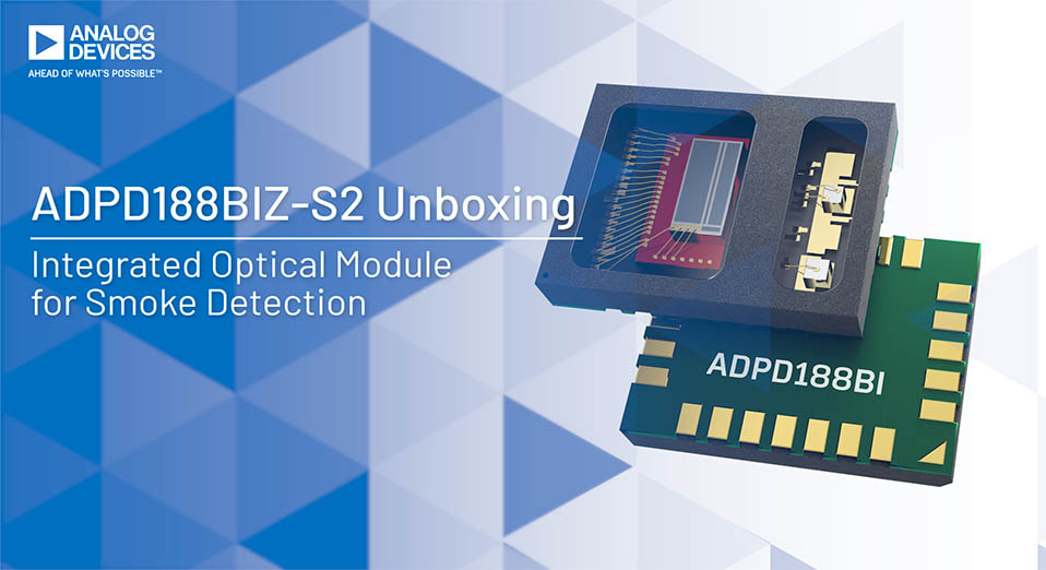
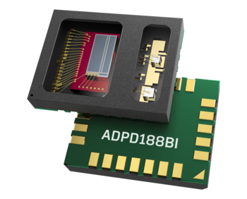
Analog Devices CN0537 Reference Design for UL-217 Smoke Detector is designed to demonstrate the use of the ADPD188BI Integrated Optical Module in a smoke/fire detection application. The ADPD188BI optical module is a complete photometric system specifically designed for smoke detection applications. Using the ADPD188BI in place of traditional, discrete smoke detector circuits greatly simplifies the design as the optoelectronics (consisting of two LEDs and two photodetectors) and the analog front end (AFE) are already integrated into the package.

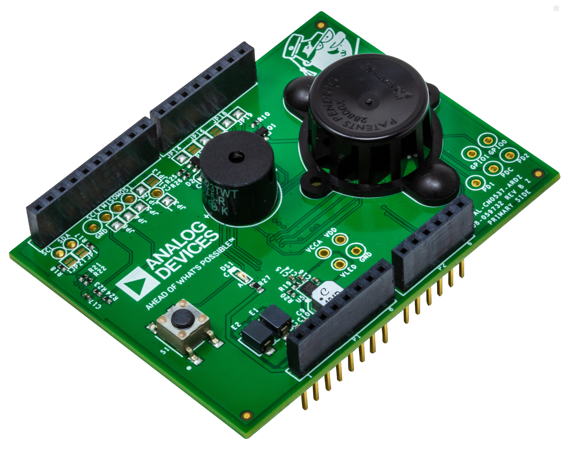
The Analog Devices Inc. CN0537 Reference Design for UL-217 Smoke Detector makes use of the EVAL-CN0537-ARDZ Evaluation Board. This Evaluation Board features a pre-mounted ADPD188BI Module, housed in a proprietary Smoke Chamber that is specifically designed to meet device and industry requirements. The internal geometry of this smoke chamber allows for the highest signal-to-noise ratio (SNR) readings and, therefore, optimal PTR values for the ADPD188BI.

When combined with the EVAL-ADICUP3029 Development Platform, the EVAL-CN0537-ARDZ Evaluation Board can be used to create a Reference Design for a smoke/fire detector circuit compliant with the ANSI/UL-217 Standard for Smoke Alarms. The UL 217 Standard includes criteria to reduce nuisance alarms and address smoke characteristics between fast-moving and smoldering fires, greatly increasing accuracy and safety.

As battery-powered devices are a common use case for smoke detectors, the Reference Design minimizes data required from the sensor and the number of computations per alarm determination. This design allows the ADPD188BI to output less data, thereby saving power and reducing consumption cycles in the microcontroller, yet still meeting the strict UL-217 specifications.

CN0537 Data & Algorithm

The Data and Algorithm Packages help complete the Reference Design. The Data Package (EVAL-CN0537-DATA) provides an extensive smoke dataset taken at UL-217 certified facilities for those who wish to develop their own algorithm and the CN0537 source code, excluding the detection algorithm. The Algorithm Package (EVAL-CN0537-ALGO) includes everything in the Data Package and a UL certified smoke detection algorithm with associated algorithm project files.

Solution Options

  • Hardware (EVAL-CN0537-ARDZEVAL-ADICUP3029) – Smoke detector reference design hardware for prototyping and solution evaluation. A tested and verified UL-217 smoke detection algorithm is embedded as part of the installer for evaluation.
    • Evaluation Board with ADPD188BI Module and Smoke Chamber
    • Microcontroller Development Board
    • UL-217 Embedded SW Executable (.hex)
    • ADPD188BI no-OS driver
  • Data (EVAL-CN0537-DATA) – CN0537 Source Code (excluding detection algorithm) plus over 1000+ sample fire/smoke datasets taken at certified UL-217 facilities for algorithm development.
    • UL-217 Test Datasets Files
    • CN0537 Source Code
    • UL-217 Test Datasets User Guide
  • Algorithm (EVAL-CN0537-ALGO) – Full source code and UL-217 8th edition tested and verified algorithm, associated project files, CN0537 source code and over 1000+ sample fire/smoke datasets to accelerate system development.
    • CN0537 Source Code including UL-217 8th Ed. Detection Algorithm (.c)
    • MATLAB and Python UL-217 Algorithm Projects
    • UL-217 Test Datasets File
    • UL-217 Algorithm Documentation
    • UL-217 Test Datasets User Guide
    • MATLAB/Python User Guide
    • 10 hours of phone support

Features

  • ADPD188BI Integrated Optical Module housed in a proprietary smoke chamber
  • Arduino Uno R3 compatible connectors
  • Selectable I2C and SPI interfaces
  • Reference Design lowers nuisance alarms using dual-wavelength detection with high SNR and dynamic range.
  • Low power circuit design for long battery life

more information: https://www.analog.com/en/design-center/reference-designs/circuits-from-the-lab/cn0537.html

LCDduino – Arduino Compatible 16X2 LCD module

The LCDduino board enables users to create many applications/projects that require a 16×2 LCD display and Arduino. The board has the exact size of 16×2 LCD and can be installed on the backside of the LCD. This is a low-cost solution that has onboard Arduino + LCD so no extra Arduino Nano or Arduino board is required. The Arduino compatible hardware includes onboard programming and boot-loader connectors, Atmega328 microcontroller, and 16×2 LCD interface. Each Arduino I/O Pin including the VCC and GND is exposed to the connectors for easy connection with sensors and other devices. The board enables the easy interface of many devices and sensors. The operating power supply is 7 to 15V DC.

LCDduino – Arduino Compatible 16X2 LCD module – [Link]

4 Channel Analog Video Distribution Amplifier

The project presented here is a low-cost video distribution amplifier capable of driving up to four video lines. The amplifier is configured with a non-inverting gain of 2. The input video source is terminated in 75 Ohms and is applied to the high impedance non-inverting input. Each output line is connected to the op-amp’s output via 75 Ohms series back termination resistor for proper cable termination. The termination resistor at the other end of the lines divides the output signal by 2, which is compensated by the gain of 2 of the op-amp. The project is built using AD8010 op-amp which is optimized for this specific function of providing excellent video performance in driving multiple video loads in parallel. Significant power is saved and heat sinking is greatly simplified because of the ability of the AD8010 to obtain this performance when running on ±5 V supply. Circuit provides 46dB of output-to-output isolation at 5Mhz driving back terminated 75 Ohms cable. Ferrite beads and high-value ceramic capacitors are used on the power supply input to reduce the noise.

4 Channel Analog Video Distribution Amplifier – [Link]

3 Channel Analog Video Splitter with Video Amplifier

If you need to drive multiple video gadgets or monitors from a single video signal source then this board is the right choice for you. This is a 3-channel video splitter with an amplifier and the circuit is built using discrete components. Q2 and Q1 act as a signal amplifier, Q3 act as output driver, trimmer potentiometer PR1 is provided to adjust the input signal swing, PR2 Trimmer is provided to set the gain of the amplifier, D1 is the power LED. The operating power supply is 12V DC and it draws 100mA current. RCA Connector J4 is the Video signal input, RCA Connector J1, J2, J3 provide the outputs. The default gain of the circuit is 4. The bandwidth is 5Mhz, input and outputs impendence are 75 Ohms. It is important to use all 3 channels at a time or change R11 to 150 Ohms if you will only use 1 x channel or 82 Ohms if 2 x channels are in use. Adjusting the board is very easy, just connect a voltmeter at the base of Q2 and adjust the PR1 so the voltage at the base of Q2 is 1V.

3 Channel Analog Video Splitter with Video Amplifier – [Link]

TOP PCB Companies