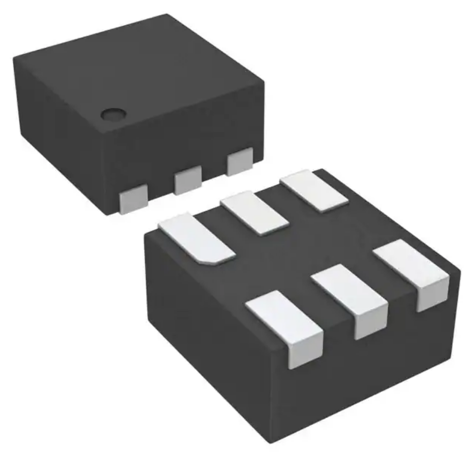
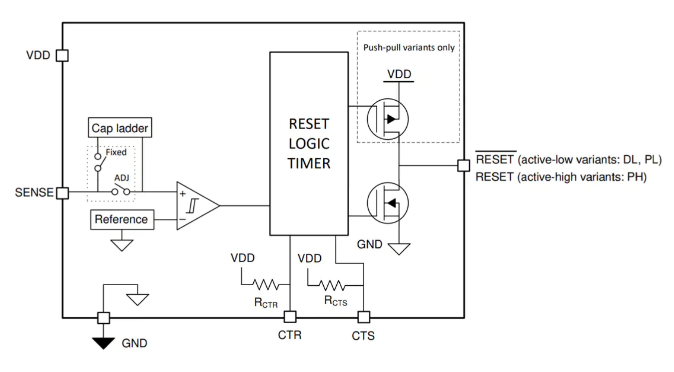
Texas Instruments TPS3899 Precision Voltage Supervisor is a nano power, precision voltage supervisor with ±0.5% threshold accuracy, programmable sense, and reset time delay in a 6-pin space-saving 1.5mm x 1.5mm WSON package. The TPS3899 is a feature-rich voltage supervisor that offers the smallest total solution size in its class. Built-in hysteresis, along with programmable delay, prevents false reset signals when monitoring a voltage rail or push-button signals.
The separate VDD and SENSE pins allow for the redundancy sought by high-reliability systems. SENSE is decoupled from VDD and can monitor rail voltages other than VDD. Optional use of external resistors is supported by the high impedance input of the SENSE pin. Both CTS and CTR provide delay adjustability on the rising and falling edges of the RESET signals. CTS also functions as a debouncer by ignoring voltage glitches on the monitored voltage rails and operates as a “manual reset” that can be used to force a system reset.
The precision performance, best-in-class features in a compact form factor makes the Texas Instruments TPS3899 an ideal solution for wide-ranging industrial and battery-powered applications such as Factory/Building Automation, Motor Drives, and consumer products. The device is fully specified over a temperature range of –40°C to +125°C (TA)
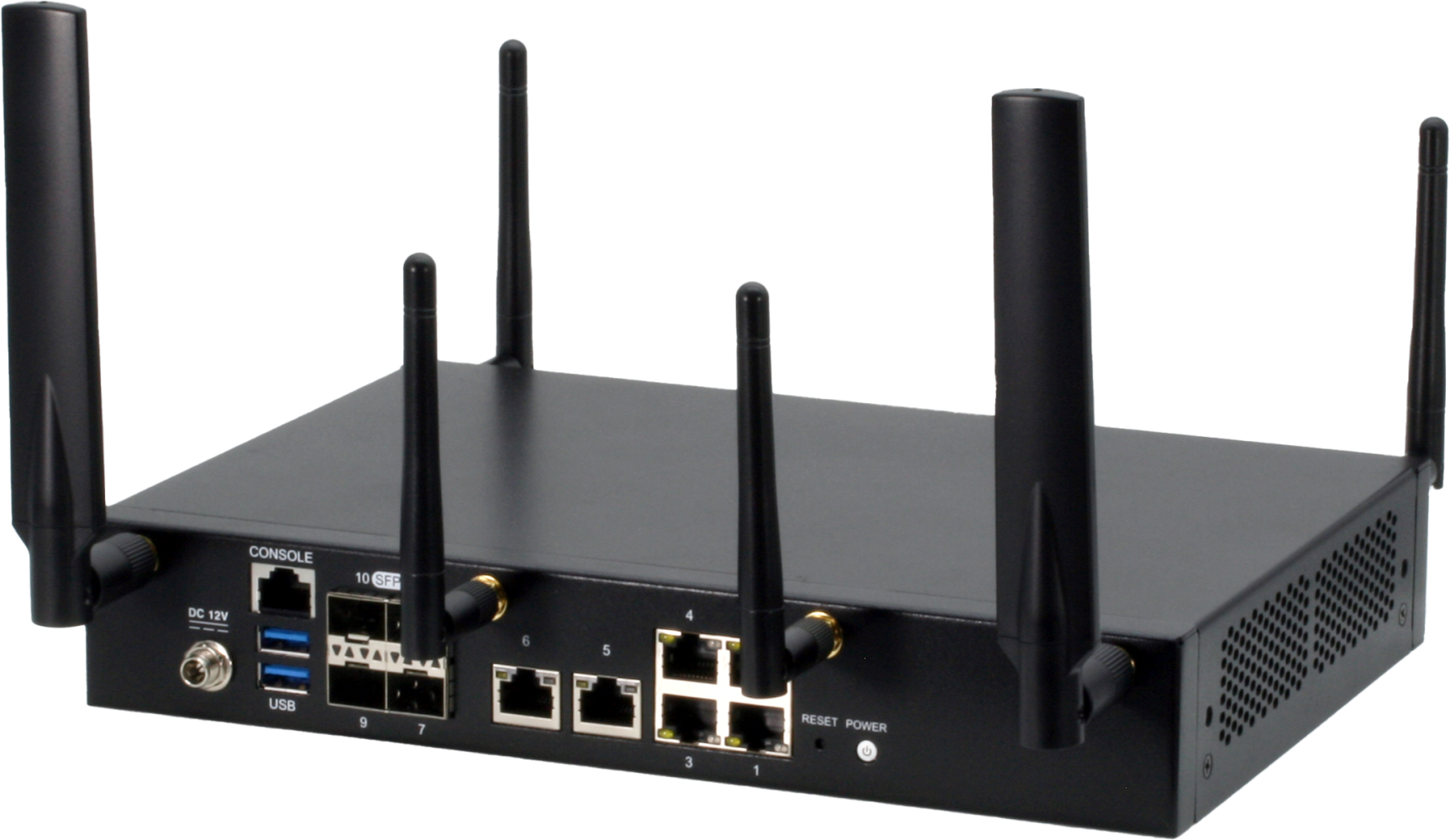
AAEON, a leading manufacturer of network appliances and white box solutions, has released the FWS-2365 desktop network appliance. Designed with a range of powerful features including 5G support and four SFP+ ports, the FWS-2365 powers faster, smarter networks for SD-WAN and uCPE applications.
The FWS-2365 is powered by Intel® Atom™ C3000 processors (formerly Denverton) with support for processors from four to sixteen cores, delivering performance to power more functions. With the Intel processors, the system supports vital performance acceleration tools including Intel QAT, SR-IOV, AES-NI, Virtualization Technology and DPDK. The FWS-2365 also supports TPM and Secure Boot to help maximize data and system security.
The FWS-2365 is built to deliver faster network speeds and higher throughput with up to four SFP+ Fiber 10 Gbps ports, and up to six copper Gigabit LAN ports, two of which can be upgraded to SFP. The FWS-2365 supports LAN Bypass functionality to provide uninterrupted connection and service.
The FWS-2365 is also built to maximize wireless performance, supporting up to three wireless expansion cards and six antennas. The FWS-2365 can support a combination of cards including Wi-Fi, 4G and 5G cellular communication. This allows for greater support for IoT connected devices and leverages the benefits of 5G to enable more flexible network structures.
Features
Intel® Atom® Processor C3000 series
10/100/1000Base-TX Ethernet x 6
Supports 1 pair bypass (LAN 3 ~ 4)
Up to 4 x 10G SFP+ Port (C3558 only supports 2 port)
DDR4 SODIMM socket x 2
SATA III Port x 2
On board 16GB eMMC, up to 128GB
Mini-card slot x 1 (Half-size, PCIe), Mini-card slot x 1 (Full-size, PCIe + USB2.0) with SIM slot
M.2 B key 3052 x 1 (USB3.0) with SIM slot
USB3.0 TypeA Port x 2 (1 Port only support USB2.0 signal)
The FWS-2365 is purpose built for white box uCPE and SD-WAN network applications. It is easy to setup and configure for a range of NFV functions such as firewall and router, as well as VPN. The FWS-2365 also supports Zero Touch Provision (ZTP) to make deployment, setup and network authorization even easier. The system also supports remote console connection for more flexible system management and monitoring.
AAEON provides industry leading service and support to ensure long lasting, reliable performance. AAEON also provides a range of manufacturer and OEM/ODM services, from software support to custom configurations and even full ground-up system design to ensure every requirement is met.
“With the combination of high core count Intel processors and focus on delivering greater speeds and throughput, the FWS-2365 is the perfect solution for white box uCPE and SD-WAN network applications,” said Fredy Hsu, Product Manager with AAEON’s Network Security Division. “With 5G connectivity and 10Gbps SFP+ support, it allows NFV, VNF vendors, and communications service providers (CSP) to accelerate deployment of SD-WAN, SD-security, QoS and other SDN/NFV applications.”
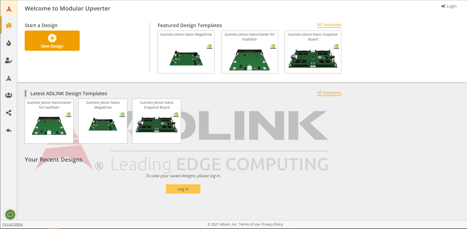
ADLINK Technology Inc., a global leader in edge computing, announces its partnership with Altium, a leader in PCB design software, to offer a fully automated SMARC carrier design process to its customers, leveraging Upverter — a web-based drag-and-drop designer tool. The Upverter tool requires minimal engineering skills, allowing customers to create their own SMARC based carrier board design within hours, and receive prototypes within weeks. Upverter generates the electrical design files of fully custom-defined carrier board designs on demand, as well as an instant Bill of Materials (BOM) complete with pricing, a customized device tree, documentation, and mechanical models.
The Upverter tool is a core component of Altium’s cloud technology platform. As Ted Pawela, Chief Ecosystem Officer, explains,
“Altium’s embeddable experiences can be added to partner websites using only a couple of lines of code. Upverter offers ADLINK’s customers a simple yet innovative way to bring new products to life.”
ADLINK’s design ecosystem called I-Pi SMARC accelerates industrial grade AIoT/IoT hardware development with standardized modular building blocks and up to 15 years longevity. The design service is available for SMARC modules based on NXP’s IMX8M and i.MX8M Plus and Rockchip’s PX30.
The ADLINK I-Pi SMARC modular approach to hardware and software addresses the aggressive timeline issue that customers face and has become the most challenging aspect of a professional engineer’s job. The I-Pi SMARC ecosystem combines industrial grade components, extreme software portability, and Raspberry Pi-like flexibility and expansion in a SMARC form factor. Fast prototyping and proof of concept are key milestones of a successful project.
“The Upverter tool is an innovative improvement of handling the proof-of-concept and prototyping phase for custom products. It will reduce the needed time to almost 50% in comparison to current approaches,” said Carsten Rebmann, Modules Product Manager at ADLINK.
Upverter is available through ADLINK’s I-Pi SMARC website starting on March 1st 2021 as a trial for interested adopters. ADLINK will release the tool for production later in 2021.
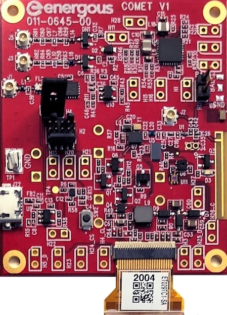
Energous and e-peas will develop an evaluation board to support at-a-distance wireless charging applications for smart buildings, industrial IoT sensors, retail electronic displays and more. (Photo: Business Wire)
Energous Corporation, the developer of WattUp®, a revolutionary wireless charging 2.0 technology, announced a partnership with e-peas S.A. (“e-peas”), a leading semiconductor company developing energy harvesting PMICs and extremely low-power microcontrollers, to develop an evaluation board combining e-peas’ power management IC technology with Energous’ radio frequency (RF) solution to support at-a-distance wireless charging applications for smart buildings, industrial IoT sensors, retail electronic displays and more.
“Our WattUp technology is designed for the growing retail, smart building and industrial IoT markets to address concerns around battery life and maintenance logistics.”
Tweet this“As a leader in at-a-distance wireless charging, we are excited to work closely with e-peas, the leading supplier of IoT energy harvesting power management and extremely low-power microcontrollers at the edge, to offer integrated solutions like this board to allow for faster evaluation of distance-based wireless charging,” said Stephen R. Rizzone, president and CEO of Energous Corporation. “Our WattUp technology is designed for the growing retail, smart building and industrial IoT markets to address concerns around battery life and maintenance logistics.”
“The results of this joint effort between Energous and e-peas will be to introduce the capabilities and advantages of a small form factor, highly integrated solution that will enable charging distances greater than one meter, eventually extending out to several meters,” said Cesar Johnston, COO and executive vice president of Energous Corporation. “The core WattUp technology supporting this evaluation board is an outgrowth of the common architecture we have developed, which emphasizes scalability for all chip, hardware, software and antenna elements of the technical solution. “
Belgium-based e-peas provides energy harvesting and processing solutions to give infinite battery life to wireless devices by increasing the amount of harvested energy and by drastically reducing the energy consumption. Key applications for e-peas solutions include smart buildings, industrial IoT sensors and retail. This evaluation board will allow companies to integrate this technology for testing and evaluation in the smart buildings, wireless sensors market and electronic displays. The wireless sensors market alone is projected to grow nearly 3x in the next four years, from $5B in 2019 to $14.6B by 2025.
“As the wireless sensors market grows, so too is the need for avoiding battery maintenance costs. That is why at-a-distance solutions capable of charging more than a meter away are critical,” said Geoffroy Gosset, CEO and co-founder of e-peas. “We believe that the combination of both Energous’ WattUp and e-peas AEM technologies on a single evaluation board will ease the deployment of zero-maintenance solutions on multiple markets.”
The evaluation board functionality is expected to include:
DA2210 WPT rectifier
E-peas AEM30940 harvesting PMIC
Supercap or rechargeable lithium battery support
Smartbond DA14531-based BLE SoC
Ambient light and temperature/humidity sensors
Support for E-Ink display charging (optional)
Support for external harvesting antenna
Energous’ WattUp wireless charging technology is based on radio frequency, which provides a number of benefits for wireless charging including the ability to be designed into small form factor products and devices without flat surfaces.
It is better to briefly revise the basic semiconductor theory before starting the PN junction theory. As we know, the N-type semiconductor has electrons as majority carrier and holes as minority carrier. The impurity in N-type semiconductor is a donor and has a bound positive charge which neutralizes majority electrons as a whole. In the same way, the P-type semiconductor has holes as a majority carrier and electrons as a minority carrier. The impurity in P-type semiconductor is acceptor and has a bound negative charge which neutralizes majority holes.
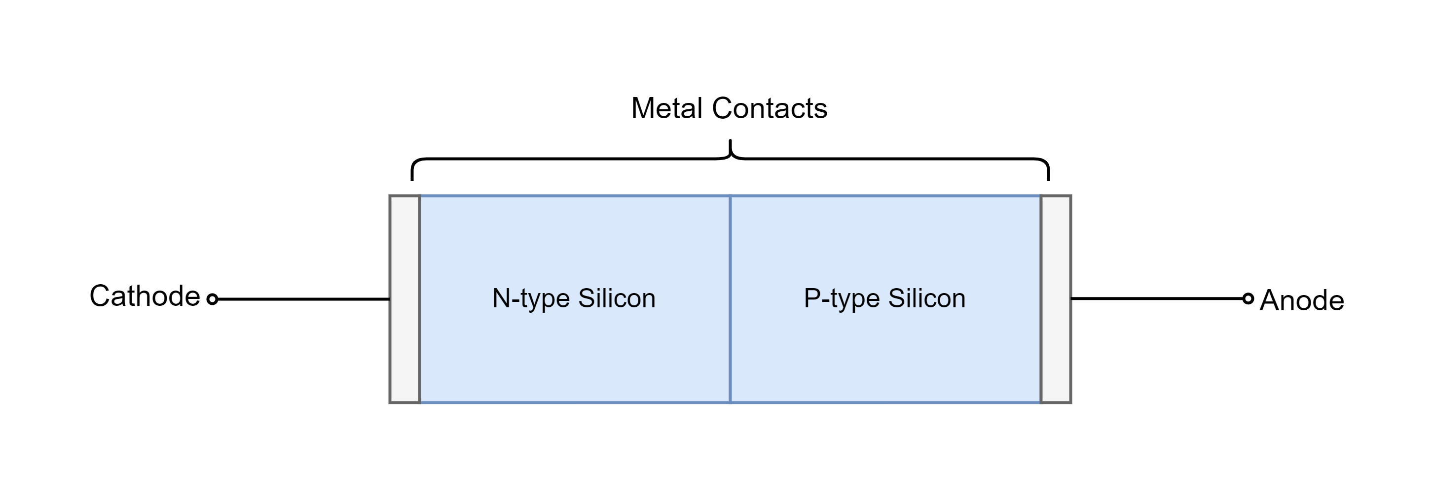
In the following figure, a physical structure of the PN junction is shown. Both P-type and N-type semiconductors are in contact with each other. Actually, both regions are made of the same silicon crystal structure/ part and this, silicon crystal, is further doped to form P-type and N-type regions. These regions are further connected to external wires through aluminum contacts. The terminals are named “anode” and “cathode” as per diode naming terminology.
Figure 1: Physical structure of PN junction with terminals “Anode” and “Cathode”.
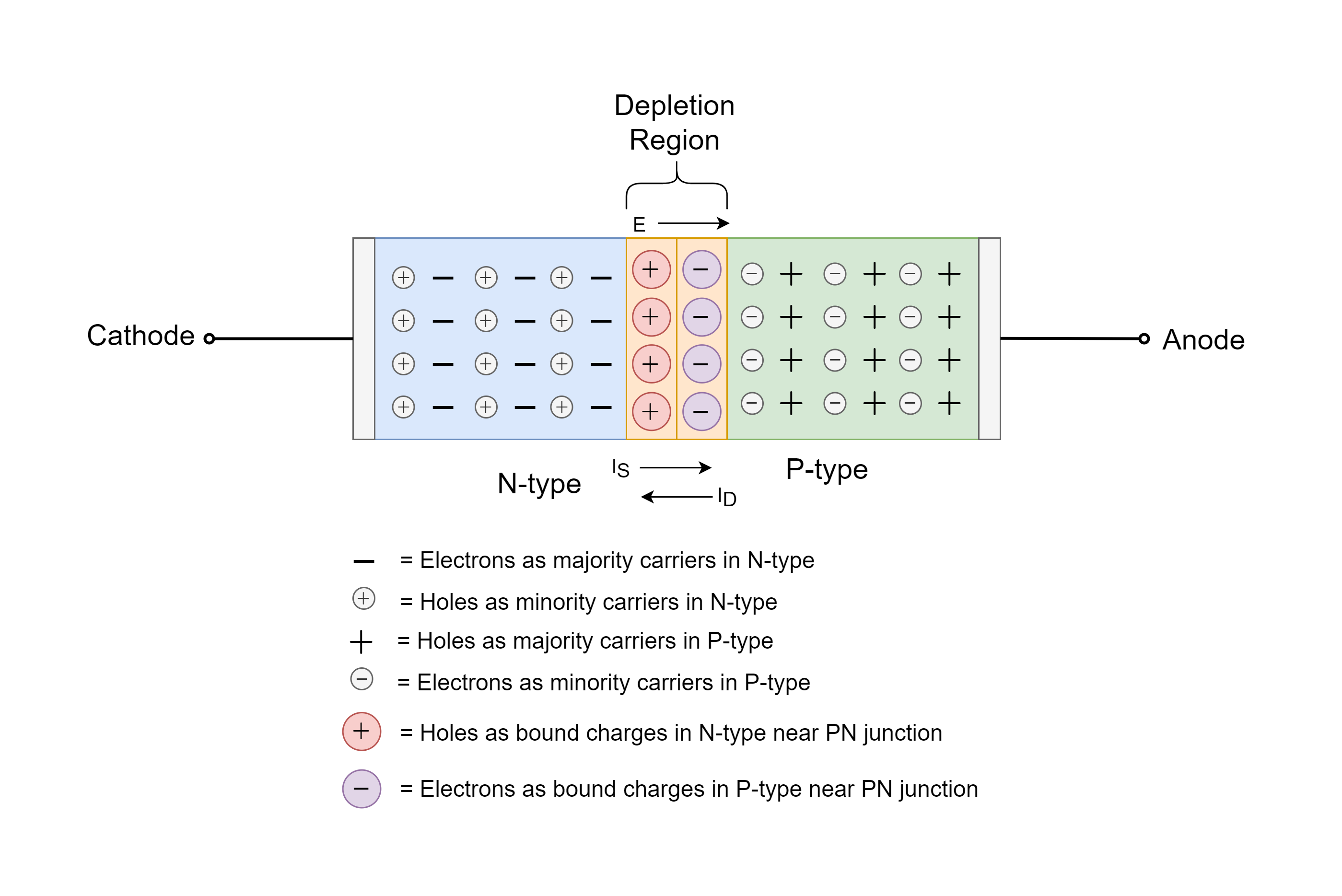
In the following figure, a PN junction is shown under the open-circuit condition which means terminals are not connected to an external voltage. Here, in the P-type region, plus “+” sign indicates holes as the majority carriers, and the circled negative “-” sign indicates the bound charge of impurity. In the N-type region, the negative “-“ sign indicates electrons which are the majority carriers, and the circled plus “+” sign indicates the bound positive charge of impurity. In the figure, thermally generated minority carriers i.e. holes and electrons in N-type and P-type regions respectively, are not shown.
Figure 2: A PN junction showing major, minor, and bound charges under open-terminal conditions.
The Diffusion Current (ID)
When the silicon crystal is doped into P-type and N-type regions then some of the majority holes and electrons diffuse in other regions due to concentration difference. The concentration of holes is high in the P-type region compared to the concentration of holes in the N-type. Similarly, the concentration of electrons is high in the N-type region compared to the concentration of electrons in the P-type. Due to this, some of the majority of electrons diffuse into P-type regions, and, similarly, some of the majority holes diffuse into the N-type region. These both diffusions constitute a diffusion current (ID) from the P-type to N-type region.
The Depletion Region
Some of the majority electrons diffusing across the PN junction to P-type region, recombine with some of the majority holes. Due to this recombination process, some of the holes disappear in the P-type region and uncover the negative bound charges of impurity. This disappearance of holes in P-type, near the PN junction, causes depletion of positive charges, and as such negative charge appears.
The majority of holes diffusing into the N-type region recombine with some of the majority electrons of the N-type and make them disappear as well. This disappearance of electrons in N-type, near the PN junction, depletes the region from electrons. This depletion uncovers the bound positive charges of impurity atoms and positive charges appear in the N-type region close to the PN- junction.
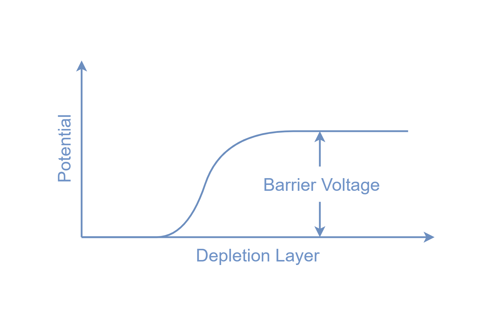
So, there is a carrier-depletion region on each side of the PN junction, the P-type will be negatively charged and the N-type will be positively charged. The formation of charges causes an electric field (E) across the depletion and a voltage appears to have N-type as positive voltage relative to P-type having negative voltage. This electric field, actually, opposes the diffusion of majority carriers into other regions and the voltage developed, due to this field, acts as a barrier. The voltage barrier has to be overcome to diffuse majority carriers into other regions. The larger the barrier voltage, the smaller the number of carriers that will be able to diffuse to constitute the diffusion current. Thus, the magnitude of diffusion current (ID) depends on the barrier voltage.
Figure 3: Barrier voltage relationship with the depletion layer.
The Drift Current (IS)
Besides, diffusion of majority carriers into other regions there is the diffusion of minority carriers into other regions as well. These minority carriers are due to thermal generation and their concentration depends on temperature. The minority holes in the N-type region, near the PN junction, experiences the electric field and diffuse into the P-type region. Similarly, the minority electrons of P-type are swept into the N-type region due to the electric field. This flow of holes from N-type to P-type and of electrons from P-type to N-type constitutes a drift current (IS). The direction of this drift current (IS) is from N-type to P-type. As the concentration of minority carriers is dependent on temperature, the drift current (IS) magnitude changes with the temperature and is independent of barrier voltage.
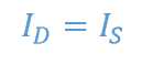
Equilibrium (ID = IS)
When this PN junction is not connected to an external voltage then under this open-circuit condition:
The diffusion current due to the depletion layer will be equal to the drift current due to thermal generation. This means that hole currents will be equal i.e. due to diffusion and drift of holes. On the other hand, electron currents will be equal i.e. due to diffusion and drift of electrons. This equilibrium condition is maintained by the depletion voltage. For example, if there is an increase in ID then the more majority carriers will diffuse into other regions which will uncover more bound charges, ultimately, widening the depletion layer. The barrier voltage will increase due to PN junction widening which will reduce ID until an equilibrium is achieved.
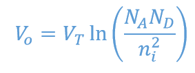
Junction Voltage
Under the open-terminal condition, the voltage across the depletion layer or the barrier voltage will be:
The above equation shows that the barrier voltage is dependent on the doping concentrations as well as on the temperature. It is worth mentioning here that for silicon, the PN-junction voltage barrier is between 0.6 V to 0.9 V, at room temperature.
Conclusion
When P-type and N-type silicon regions are combined then the majority carriers of each region diffuse into other regions.
Electrons of the N-type region diffuse into the P-type and holes from the P-type diffuse into the N-type region.
Diffusion of these majority carriers into other regions constitutes a diffusion current (ID).
The majority carriers diffusing into other regions recombine with opposite majority charges and make them disappear. Which uncovers the bound charges.
Electrons diffusing from N-type to P-type recombine with holes (which make holes disappear) uncovering bound negative charges of impurity atoms.
Holes diffusing from P-type to N-type recombine with electrons (which make electrons disappear) uncovering bound positive charges of impurity atoms.
Adjacent to the PN junction, positive charges appear in N-type and negative charges in P-type regions.
The appearance of these bound charges establishes an electric field (E) and barrier voltage (VO).
Barrier voltage (VO) opposes diffusion of majority charges only.
Thermally generated minority carriers diffuse into other regions as well but in opposite direction to the majority carriers, giving rise to drift current (IS).
In equilibrium (open-terminal condition)
ID = IS
The magnitude of drift current (IS) depends on temperature.
In open-terminal condition, barrier voltage establishes equilibrium by either increasing or decreasing the diffusion current (ID).
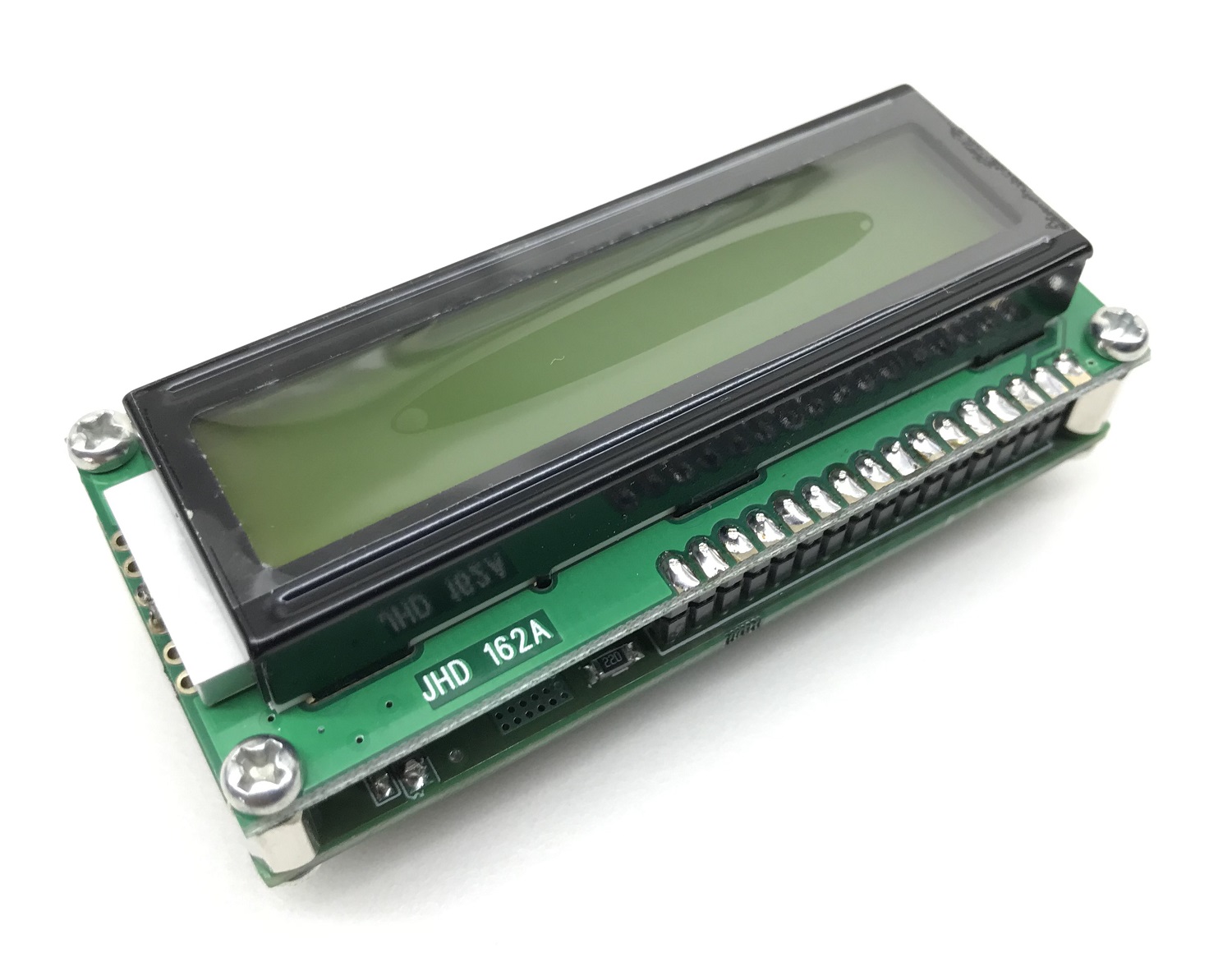
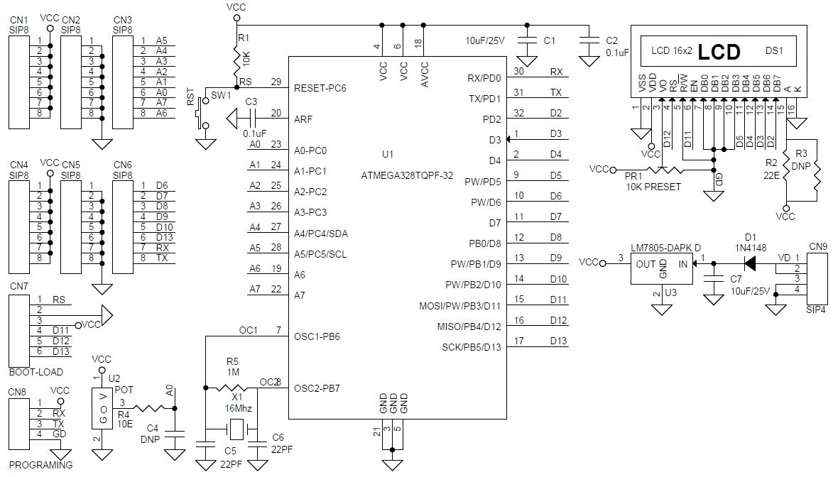
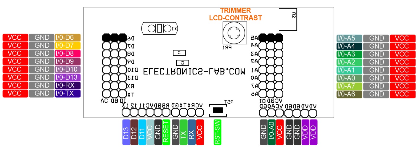
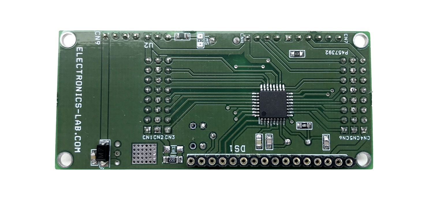
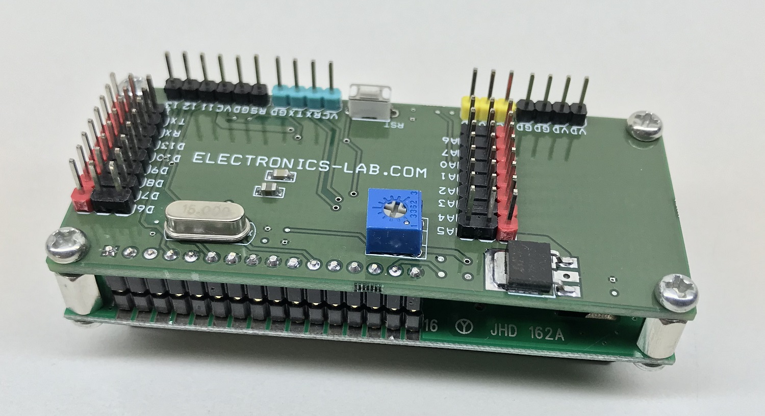
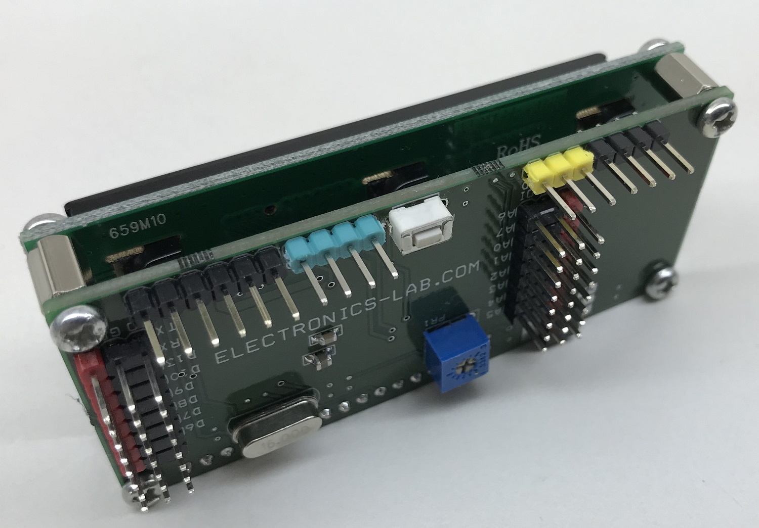
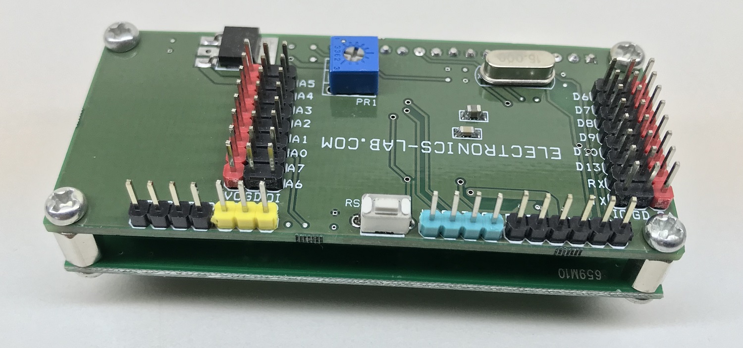
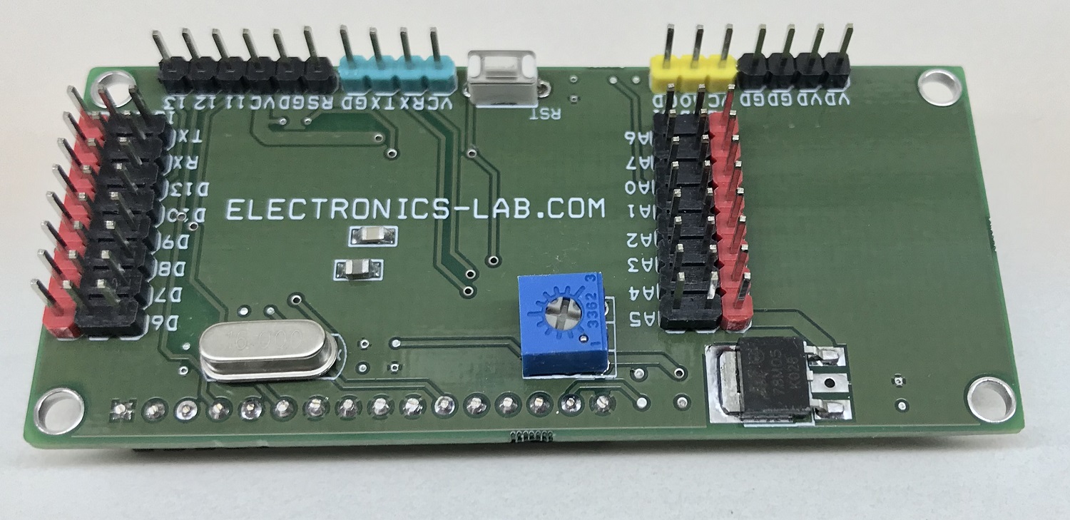
The LCDduino board enables users to create many applications/projects that require a 16×2 LCD display and Arduino. The board has the exact size of 16×2 LCD and can be installed on the backside of the LCD. This is a low-cost solution that has onboard Arduino + LCD so no extra Arduino Nano or Arduino board is required. The Arduino compatible hardware includes onboard programming and boot-loader connectors, Atmega328 microcontroller, and 16×2 LCD interface. Each Arduino I/O Pin including the VCC and GND is exposed to the connectors for easy connection with sensors and other devices. The board enables the easy interface of many devices and sensors. The operating power supply is 7 to 15V DC.
Key features:
Arduino Compatible Hardware
Operating Power Supply 7 to 15V DC (VDD-GND Pins) or 5V DC (VCC-GND Pins)
Arduino Digital Pin D2, D3, D4, D5, D11, D12 connected to 16×2 LCD
Arduino Digital Pin D6, D7, D8, D9, D10, D13, D0, D1 I/O Pins are available for external Interface
Arduino Analog Pin A0, A1, A2, A3, A4, A5, A6, A7 Pins are available for external interface
Each Digital and Analog Pin includes VCC and GND for easy interface to external sensor and device
On-Board 5V Regulator
On-Board Trimmer Potentiometer to set the Contrast of LCD
On-Board Current Limiting Resistor R2/R3 for LCD Back Light
On-Board Reset Switch
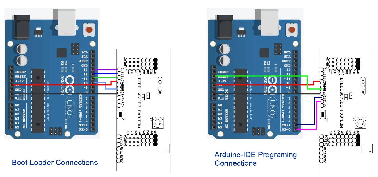
On-Board Bootloader Burning Connector for New ATmega328 Micro-controller (D10, D11, D12, D13, VCC and GND Pins)
On-Board Arduino IDE Programming Connector (RX, TX, Reset, VCC and GND Pins)
4 x Mounting Holes 3.2mm Diameters
PCB Dimensions 80 x 35.72 mm
Programming the Atmega328
After the board assembly, the brand new Atmega328 microcontroller requires burning the bootloader before it can be programmed using Arduino IDE. Refer to the connection diagram and follow the links below to learn more about bootloader and Arduino IDE programming.
Arduino example code is provided below to test the project. This code will help you to convert this board into a 0 to 5V Voltmeter. Just connect the DC source at analog in A0 to measure the DC voltage.
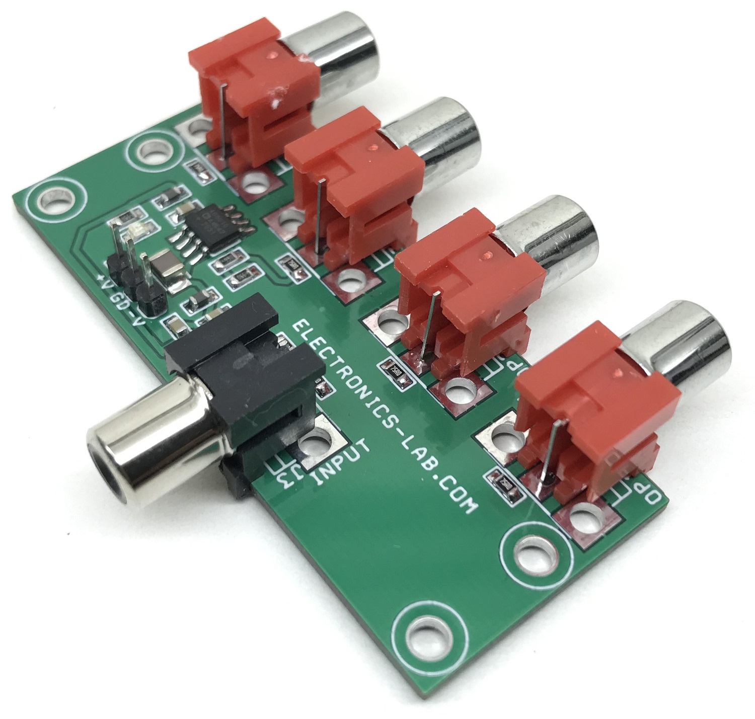
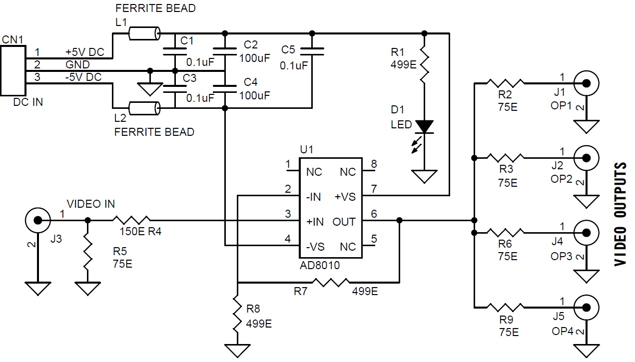
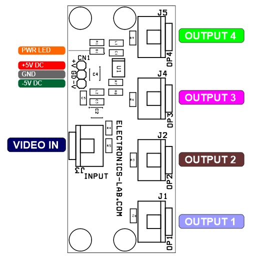
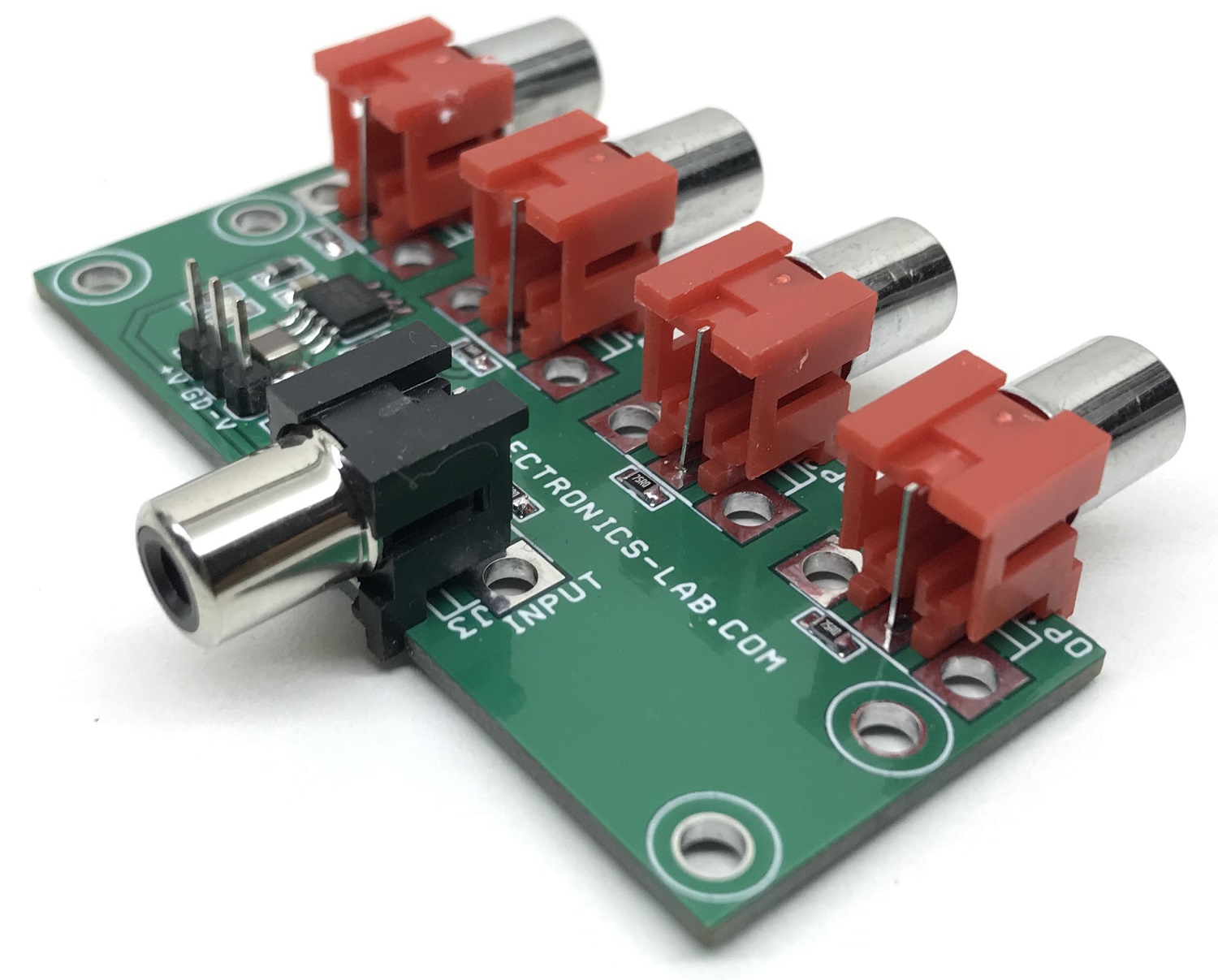
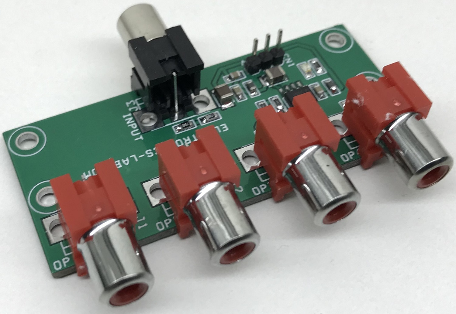
The project presented here is a low-cost video distribution amplifier capable of driving up to four video lines. The amplifier is configured with a non-inverting gain of 2. The input video source is terminated in 75 Ohms and is applied to the high impedance non-inverting input. Each output line is connected to the op-amp’s output via 75 Ohms series back termination resistor for proper cable termination. The termination resistor at the other end of the lines divides the output signal by 2, which is compensated by the gain of 2 of the op-amp. The project is built using AD8010 op-amp which is optimized for this specific function of providing excellent video performance in driving multiple video loads in parallel. Significant power is saved and heat sinking is greatly simplified because of the ability of the AD8010 to obtain this performance when running on ±5 V supply. Circuit provides 46dB of output-to-output isolation at 5Mhz driving back terminated 75 Ohms cable. Ferrite beads and high-value ceramic capacitors are used on the power supply input to reduce the noise.
Features
Power Supply +/-5V DC (Dual 5V Symmetrical Power Supply) @ 20mA
RCA Connector for Video In
4 x RCA Connector for Video Output
Power LED
PCB Dimensions 69.06 x 29.69 mm
The AD8010 is a low-power, high current amplifier capable of delivering a minimum load drive of 175 mA. Signal performance such as 0.02% and 0.03° differential gain and phase error is maintained while driving eight 75 Ω back terminated video lines. The current feedback amplifier features gain flatness to 60 MHz and –3 dB (G = +1) signal bandwidth of 230 MHz and only requires a typical 15.5 mA supply current from ±5 V supplies. These features make the AD8010 an ideal component for Video Distribution Amplifiers.
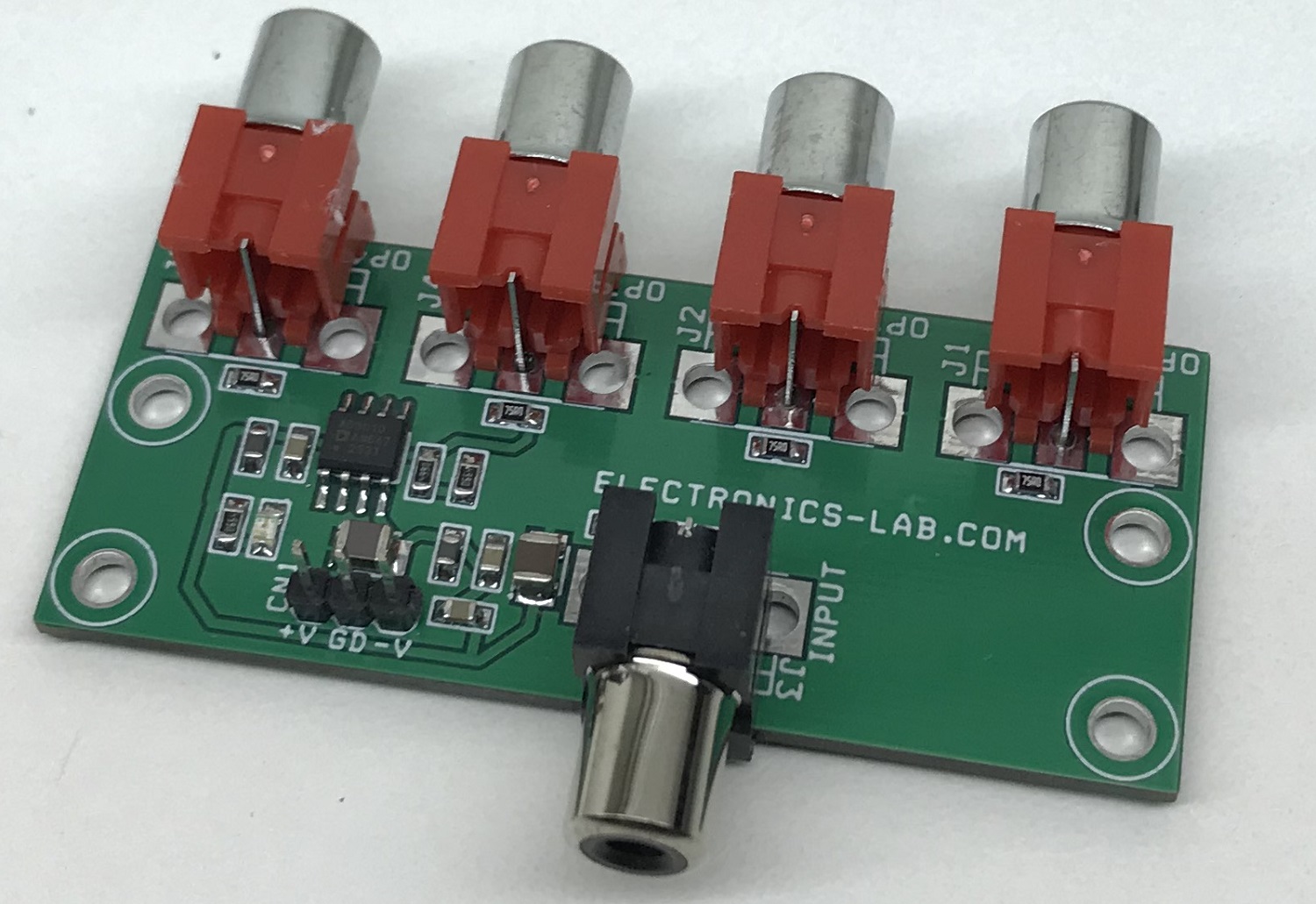
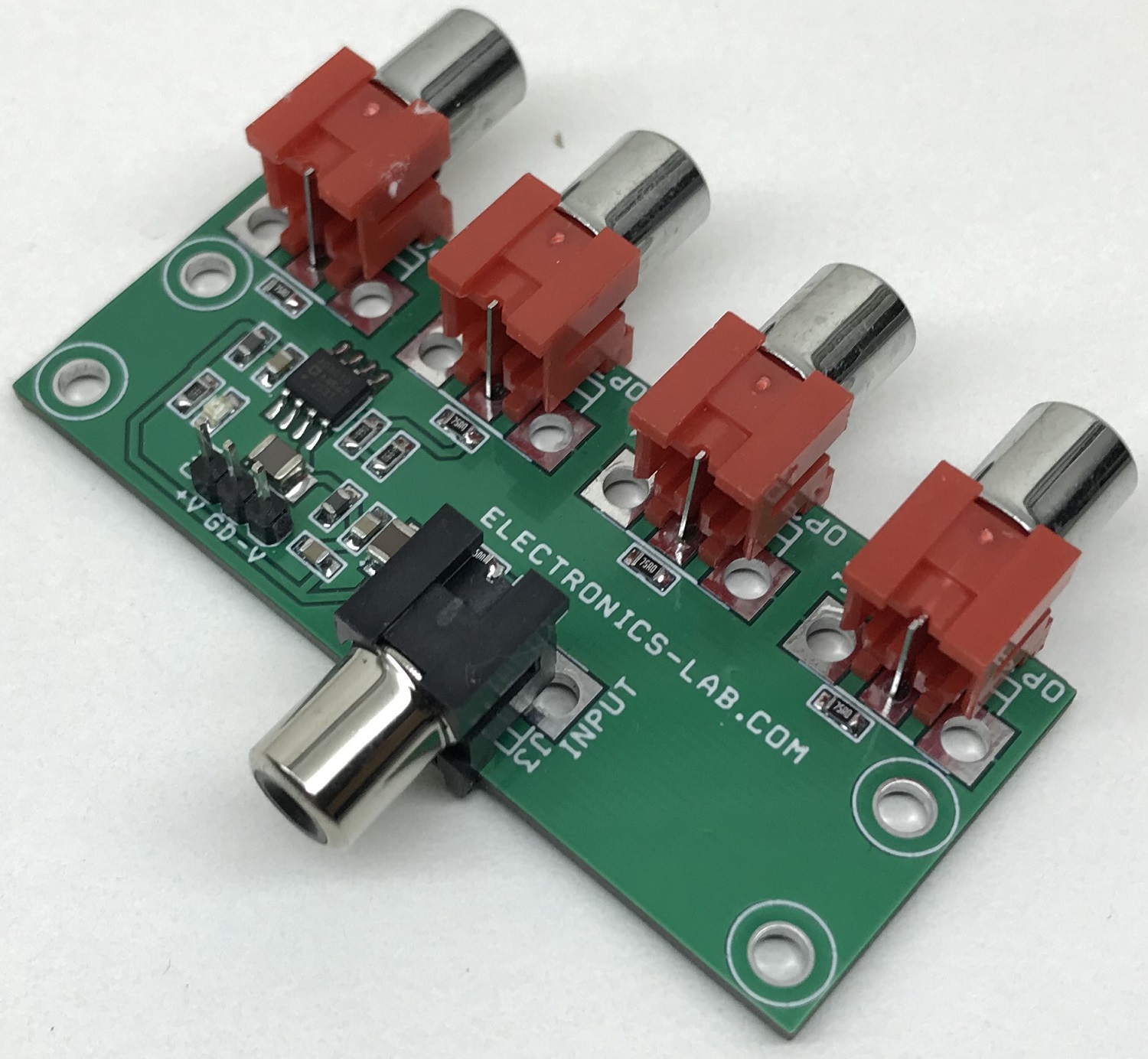
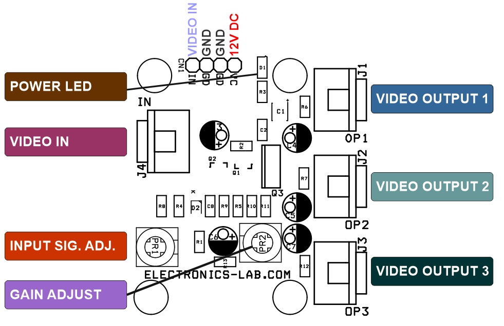
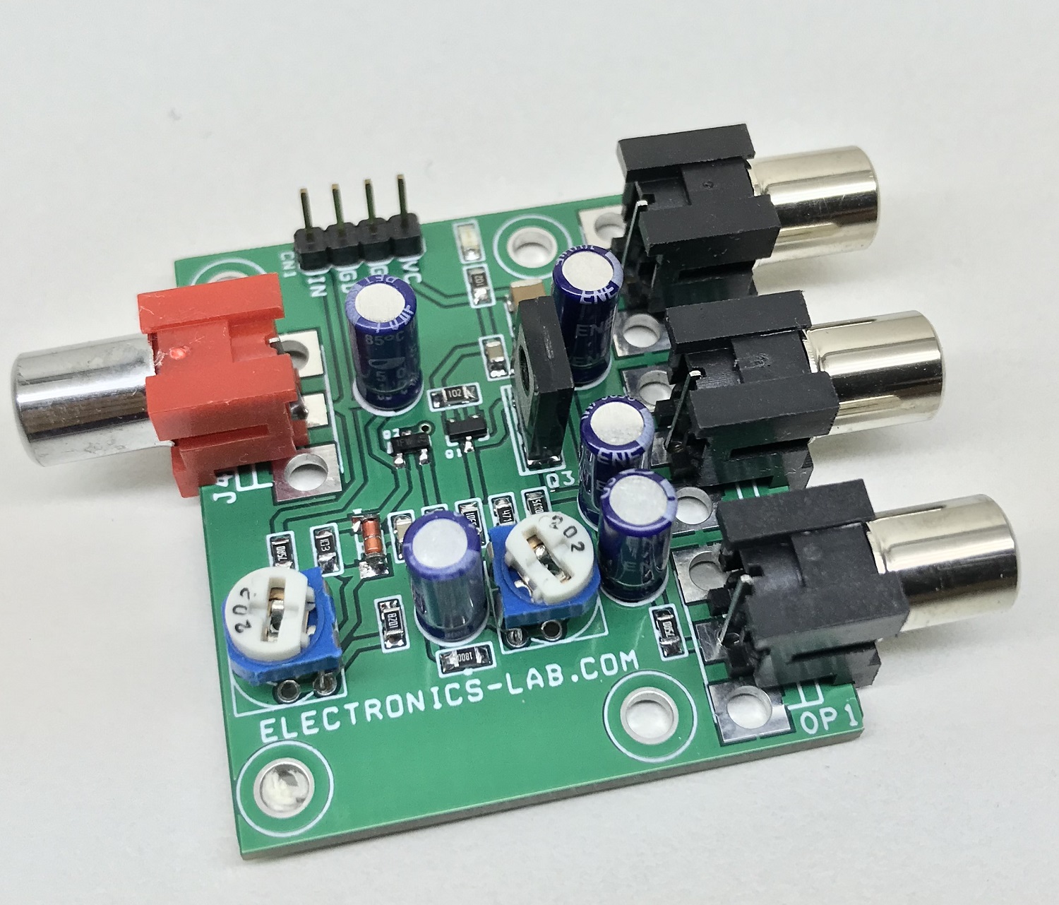
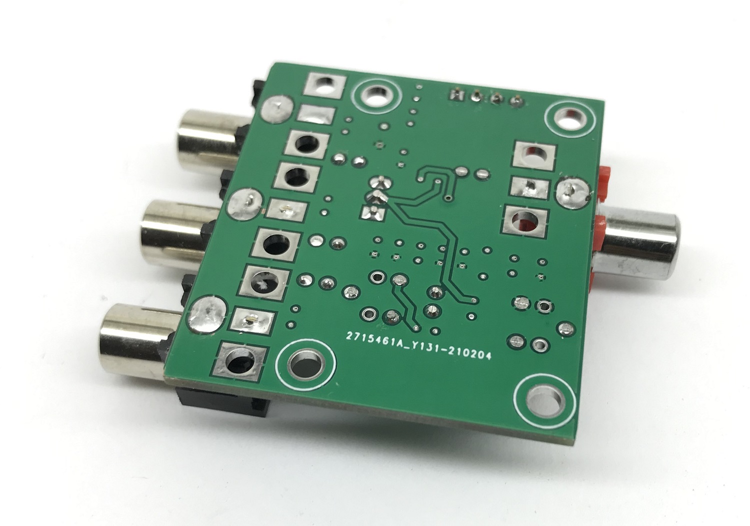
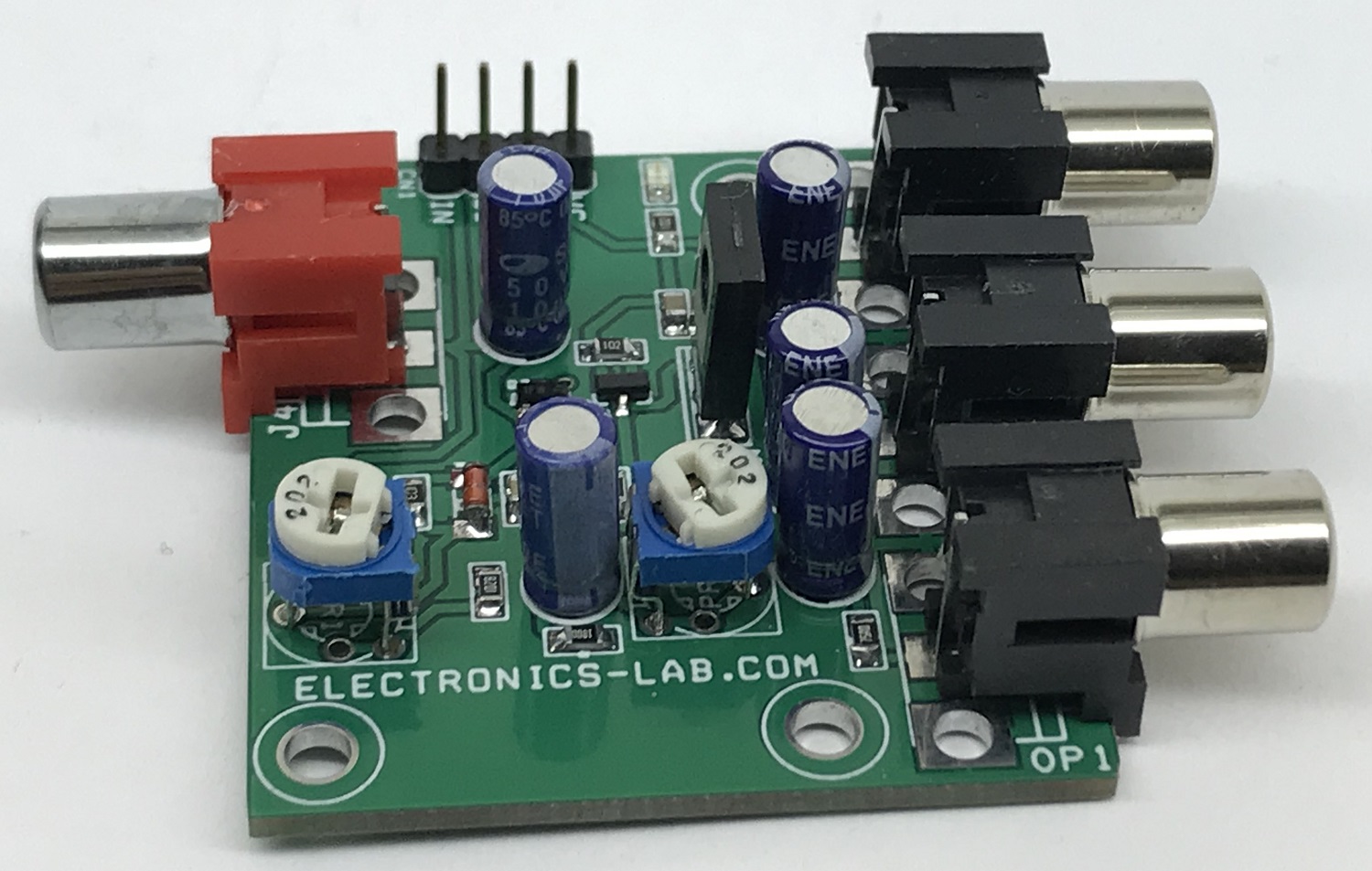
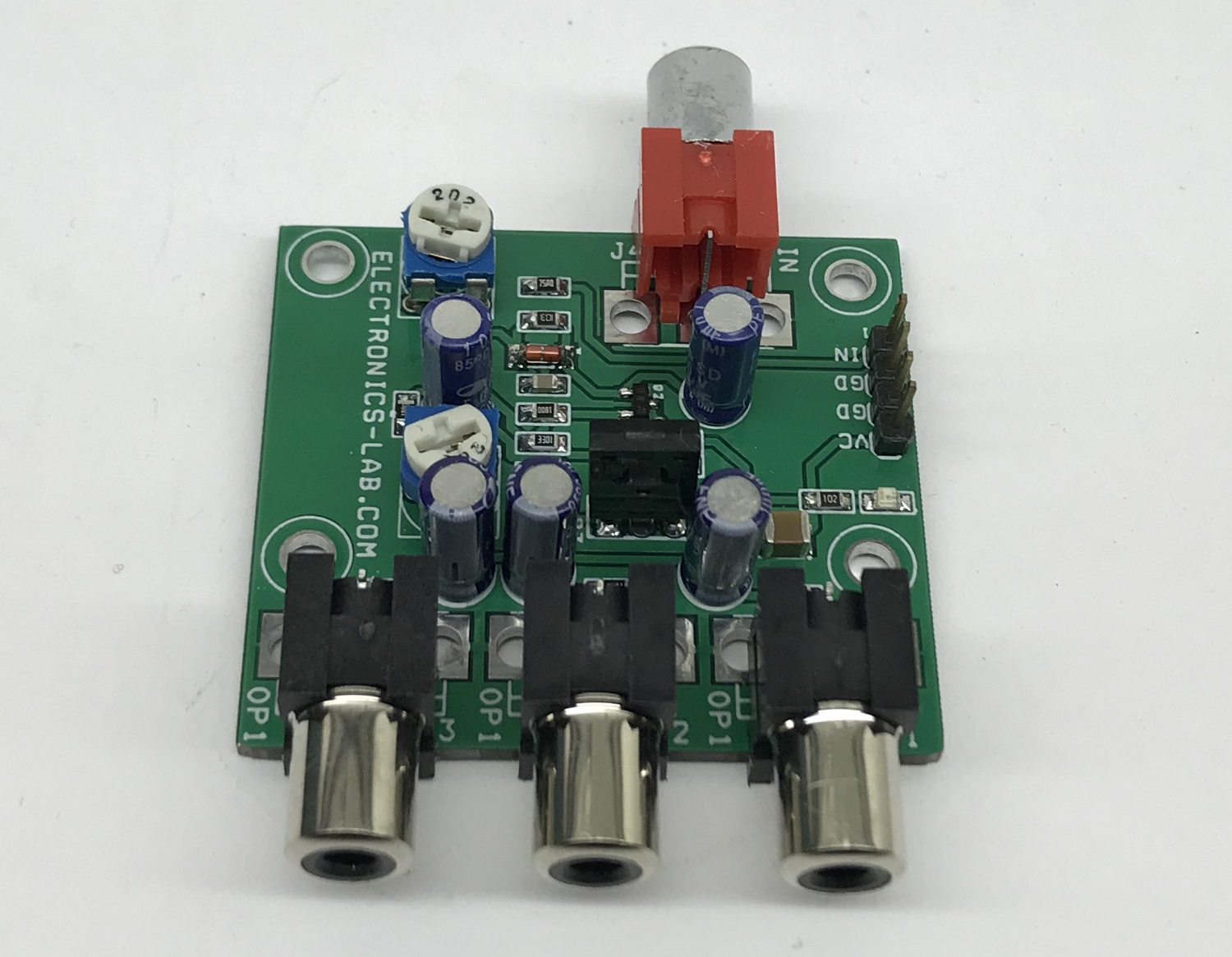
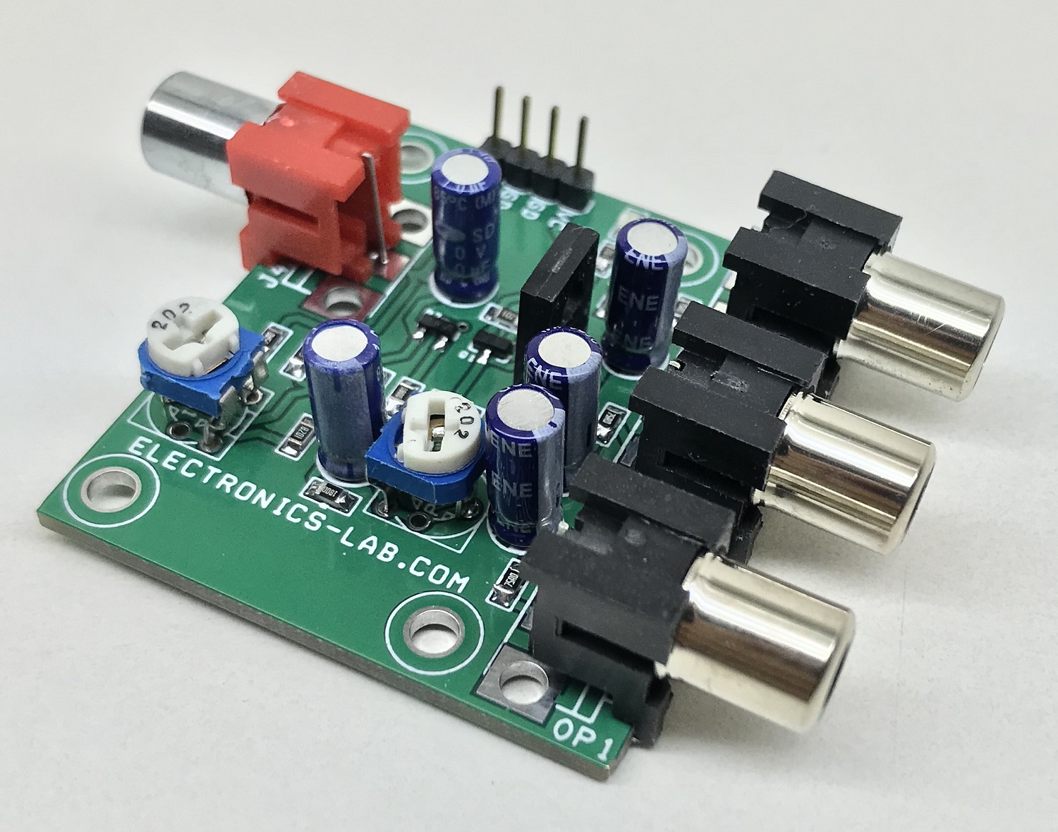
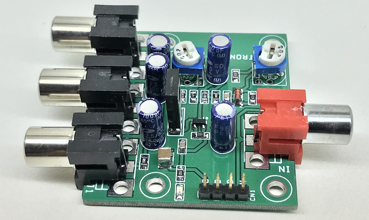
If you need to drive multiple video gadgets or monitors from a single video signal source then this board is the right choice for you. This is a 3-channel video splitter with an amplifier and the circuit is built using discrete components. Q2 and Q1 act as a signal amplifier, Q3 act as output driver, trimmer potentiometer PR1 is provided to adjust the input signal swing, PR2 Trimmer is provided to set the gain of the amplifier, D1 is the power LED. The operating power supply is 12V DC and it draws 100mA current. RCA Connector J4 is the Video signal input, RCA Connector J1, J2, J3 provide the outputs. The default gain of the circuit is 4. The bandwidth is 5Mhz, input and outputs impendence are 75 Ohms. It is important to use all 3 channels at a time or change R11 to 150 Ohms if you will only use 1 x channel or 82 Ohms if 2 x channels are in use. Adjusting the board is very easy, just connect a voltmeter at the base of Q2 and adjust the PR1 so the voltage at the base of Q2 is 1V.
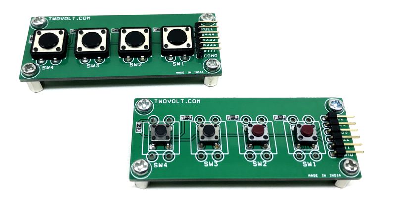
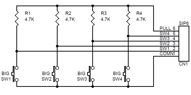
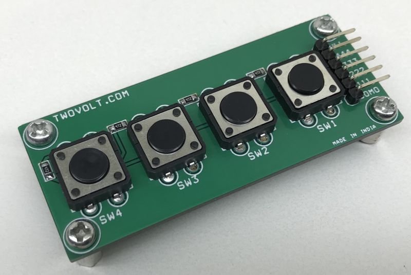
This breadboard-friendly board breaks out all 4 tactile switch signals and includes pullup resistors configured so that the outputs read low or high when configured common VCC or GND.
BoschBME688 AI Gas Sensor offers a 1.2V to 3.6V supply voltage range and 3mm x 3mm x 0.93mm3 package dimensions. This sensor features integrated high linearity and high-accuracy pressure, humidity, and temperature sensors. The BME688 gas sensor can detect Volatile Organic Compounds (VOC) and other gases such as hydrogen and carbon monoxide in the part per billion (ppb) range. Bosch BME688 AI Gas Sensor is ideal for mobile and connected applications where size and low power consumption are critical requirements.