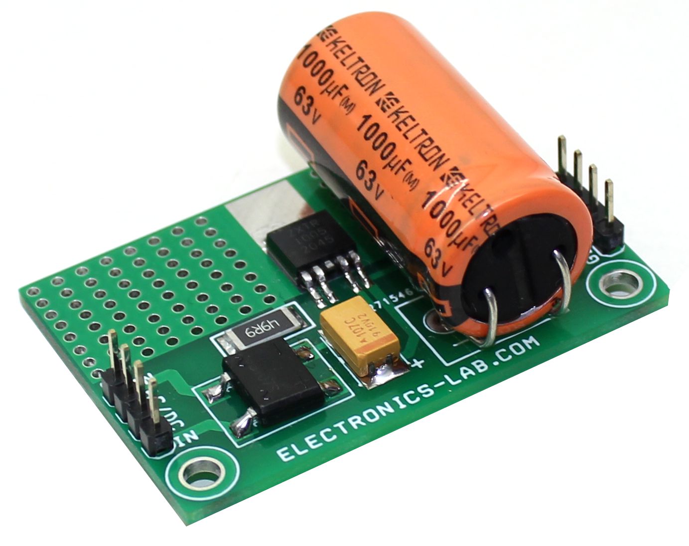
This is a high voltage regulator project that provides 5V regulated output with a load capacity of 50mA from input supply 10V to 60V. The project is based on the ZXTR1005K4 regulator which is fully integrated into a TO252 package. We have tested this project with 60V DC input, but the project can take higher voltage input up to 100V, please refer to the datasheet below for more info, and don’t forget to change the capacitor C1 with a higher voltage rating.
60V Input – 5V @ 50mA Output High Voltage Fixed Output Regulator – [Link]
New chipset completes Sony’s Altair Cellular IoT solution portfolio to address NB only and NB/2G applications
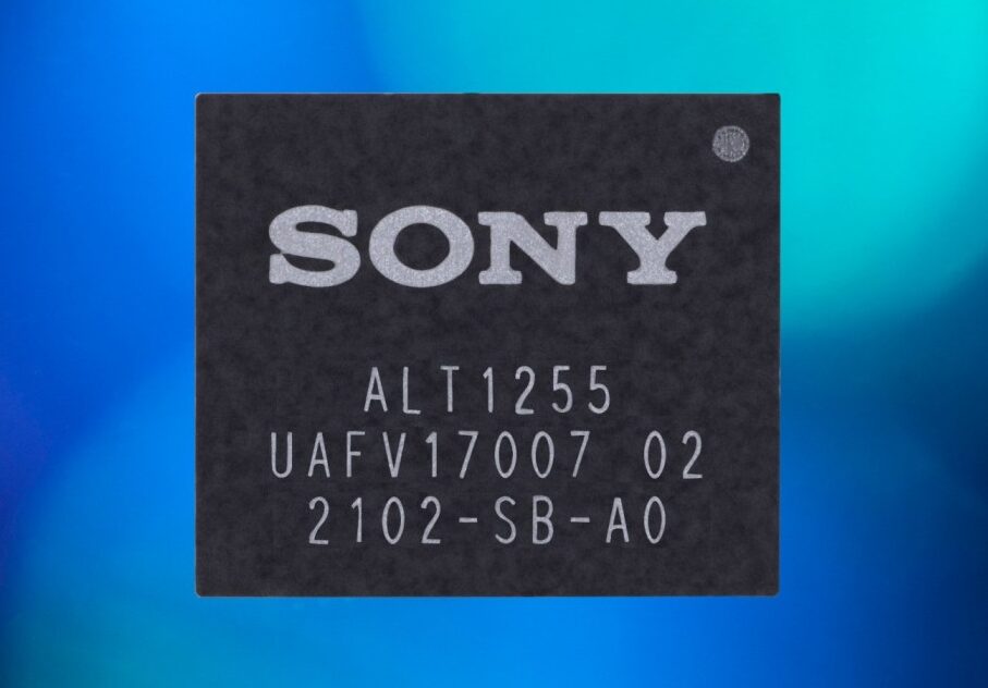
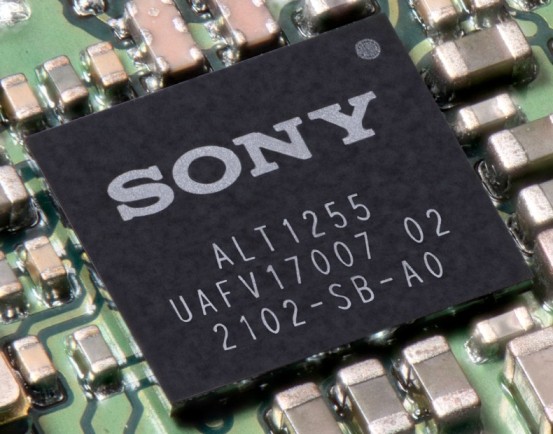
Sony Semiconductor Israel (Sony), a leading provider of cellular IoT chipsets, announced the launch of the Altair ALT1255, a new low-power NB2 chipset. The ALT1255 is 5G ready, designed with an integrated SIM (iSIM), user MCU, rich application layer, and GSM/GPRS fallback modem.
The ALT1255 chipset empowers device manufacturers to develop low-power, cost-sensitive connected devices at a global scale to monitor, manage, and control critical infrastructure, medical devices, logistic trackers, and a large variety of LPWA applications.
The ALT1255 platform is now commercially available and has been selected by key module players.
The ALT1255 was developed in-house by Sony Semiconductor Israel, based on the LTE-M/NB ALT1250 chipset, and leverages its mature, broadly accepted, and globally certified NB/2G technology. The chipsets share software architecture, modem application and networking layer, and APIs for fast and easy integration within the Altair product family.
“The market shows a growing need for a feature-rich, fully integrated NB-IoT cellular chipset with 2G fallback,” said Dima Feldman, VP of Product Management and Marketing at Sony Semiconductor Israel. “Module designs based on the ALT1255 will provide reliable connectivity for smart meters, logistics, telematics, and smart cities applications.”
The ALT1255 built-in iSIM removes barriers related to cost, size, and power, as well as adds an additional layer of security. The GSM/GPRS modem fills the gaps in LPWA network coverage and allows future-proof technology deployment in countries with mixed 2G/NB coverage. In addition, ALT1255 integrates a low-power ARM Cortex-M4 MCU, fully separated from the modem functionality and designed to run a variety of IoT and sensing applications, as well as an adaptation layer to interconnect within the existing ecosystem.
The solution provides out-of-the-box secure cloud connectivity, utilizing numerous industry-accepted communication protocols such as power-efficient COAP and LWM2M.
As part of Sony’s Altair family of products, the ALT1255 is trusted by carriers, iSIM ecosystem partners, and developers designing IoT devices and have already received broad acceptance across the industry.
The chipset has received the Global Certification Forum (GCF) certification, which allows customers to accelerate module and device certification.
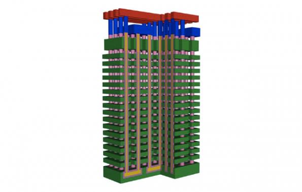
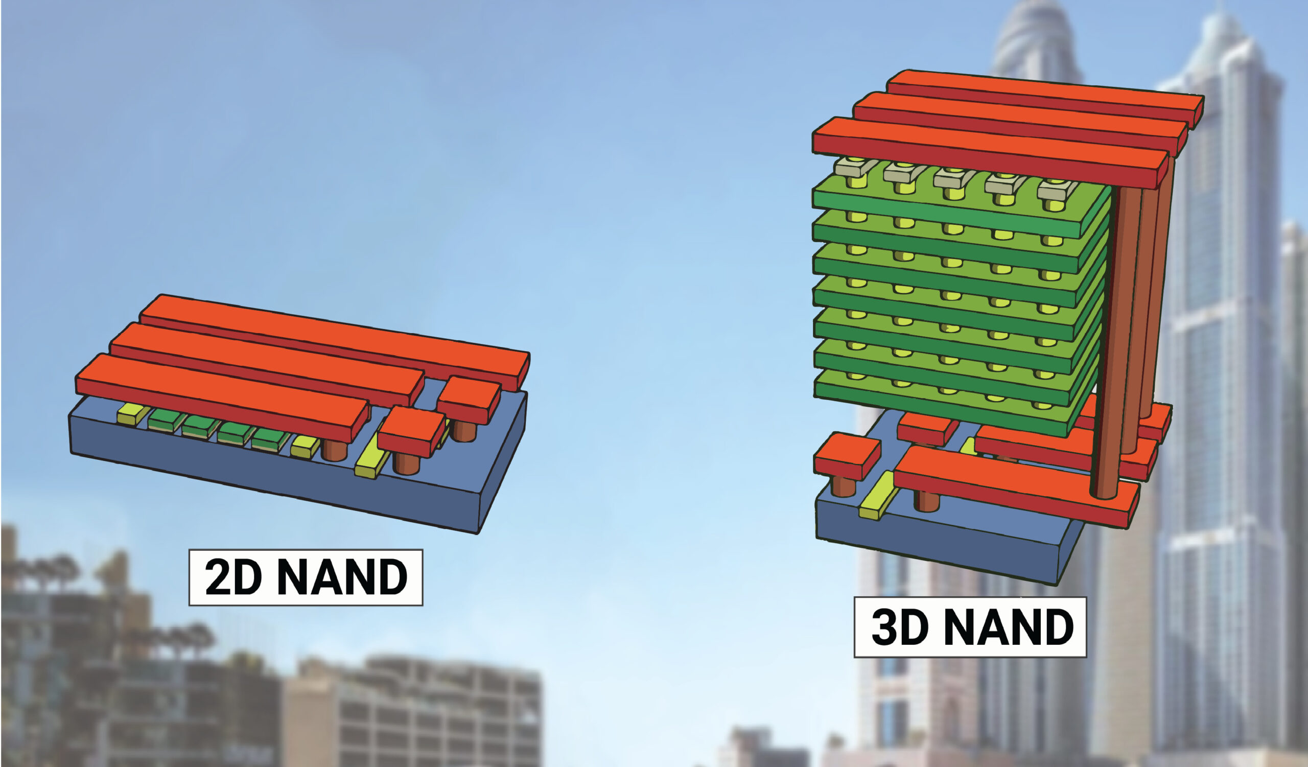
Kioxia Corporation and Western Digital Corp., today announced that the companies have developed their sixth-generation, 162-layer 3D flash memory technology. Marking the next milestone in the companies’ 20-year joint-venture partnership, this is the companies’ highest density and most advanced 3D flash memory technology to date, utilizing a wide range of technology and manufacturing innovations.
“Through our strong partnership that has spanned two decades, Kioxia and Western Digital have successfully created unrivaled capabilities in manufacturing and R&D,” said Masaki Momodomi, Chief Technology Officer, Kioxia. “Together, we produce over 30 percent1 of the world’s flash memory bits and are steadfast in our mission to provide exceptional capacity, performance and reliability at a compelling cost. We each deliver this value proposition across a range of data-centric applications from personal electronics to data centers as well as emerging applications enabled by 5G networks, artificial intelligence and autonomous systems.”
Beyond Vertical Scaling – New Architecture Leverages New Innovations
“As Moore’s Law reaches its physical limits across the semiconductor industry, there’s one place where Moore’s Law continues its relevancy — that’s in flash,” said Dr. Siva Sivaram, President of Technology & Strategy, Western Digital. “To continue these advances and meet the world’s growing data demands, a new approach to 3D flash memory scaling is critical. With this new generation, Kioxia and Western Digital are introducing innovations in vertical as well as lateral scaling to achieve greater capacity in a smaller die with fewer layers. This innovation ultimately delivers the performance, reliability and cost that customers need.”
This sixth-generation 3D flash memory features advanced architecture beyond the conventional eight-stagger memory hole array and achieves up to 10 percent greater lateral cell array density compared to the fifth-generation technology. This lateral scaling advancement, in combination with 162 layers of stacked vertical memory, enables a 40 percent reduction in die size compared to the 112-layer stacking technology, optimizing cost.
The Kioxia and Western Digital teams also applied Circuit Under Array CMOS placement and four-plane operation, which together deliver nearly 2.4 times improvement in program performance and 10 percent improvement in read latency compared to the previous generation. I/O performance also improves by 66 percent, enabling the next-generation interface to support the ever-increasing need for faster transfer rates.
Overall, the new 3D flash memory technology reduces the cost per bit, as well as increases the manufactured bits per wafer by 70 percent, compared with the previous generation. Kioxia and Western Digital continue to drive innovation to ensure continued scaling to meet the needs of customers and their diverse applications.
The companies detailed the related innovations in a joint presentation at the ISSCC 2021 show earlier today.
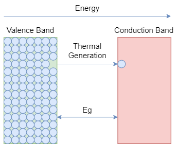
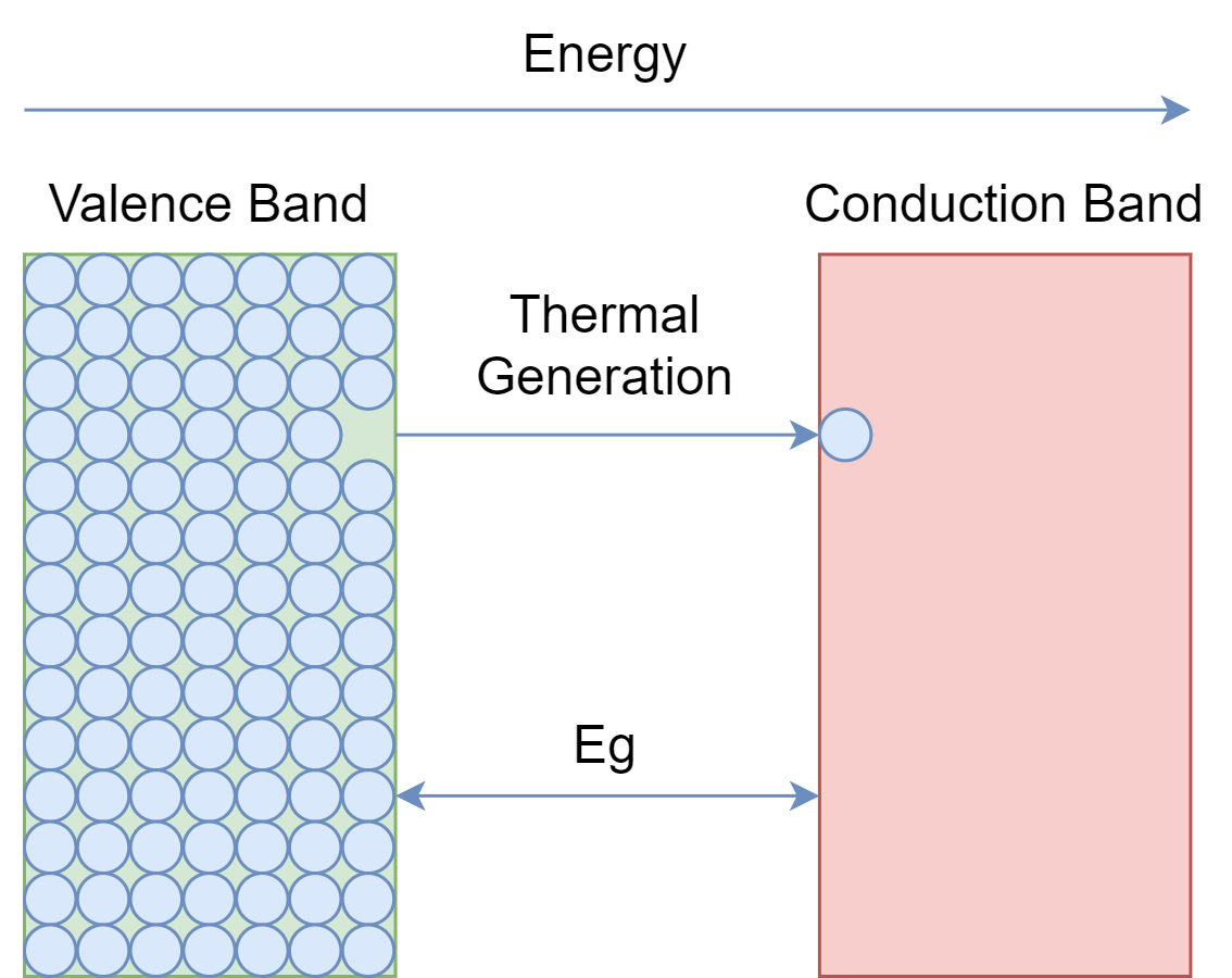
As it is obvious from the name, semiconductors are those materials having conductivity in between conductors and insulators. Conductors are those materials that impose minimum resistance in the flow of electrons or current. Whereas, insulator materials impose high resistivity and, thus, no current flows in them. As we know, for an atom, there are valence electrons, and when they gain a sufficient amount of energy they jump into the conduction band. The forbidden band is there in between these valence and conduction bands. The flow of current is due to the presence of free electrons in the conduction band.
In conductors, the valence band and conduction band overlap with each other, and electrons require a minimum amount of energy to jump into the conduction band. The good conductors are Copper, Silver, and Aluminum. Insulators have wider forbidden energy gaps and electrons require a significant amount of energy to shift into the conduction band. Therefore, insulators have poor conductivity as there are no electrons in the conduction band. The good insulators are glass, porcelain, rubber, and ceramics.
The forbidden energy gap in semiconductors is not that wide, as in insulators, nor it is overlapping, as in conductors. It is somewhere, in between, and at room temperature valence electrons of the semiconductor get enough energy to jump into the conduction band. However, the number of electrons jumping into the conduction band is not that much to cause a good current flow. Examples of semiconductors are Silicon, Germanium, and Germanium Arsenide.
Figure 1: Band gap energy between valence and conduction bands.
Semiconductors are of two kinds: single-element, such as Silicon and Germanium; and compound semiconductors, such Gallium-Arsenide. The compound semiconductors are used in some special electronic applications such as in devices involving light e.g. LEDs diodes.
Intrinsic Semiconductors
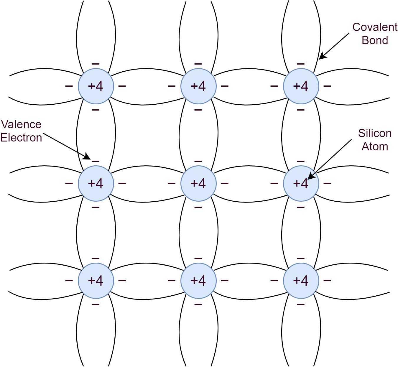
An intrinsic semiconductor is a pure form of a semiconductor material such as Silicon or Germanium. Silicon belongs to Group-IV of the periodic table and as such has four valence electrons. These four valence electrons form covalent bonds with the valence electrons of neighboring atoms. This makes a pure crystal of regular lattice structure.
Figure 2: Intrinsic Silicon crystal structure.
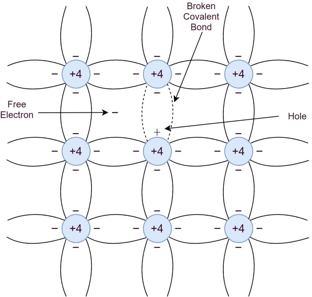
At low temperatures, near to absolute zero (0K), the covalent bonds remain strong enough to make Silicon act as an insulator. However, due to thermal generation, energy is sufficient enough to break some of the covalent bonds at room temperature and create free electrons. Silicon crystal structure when subjected to an electric field or potential, makes free electrons to conduct electricity. The freed electron leaves behind a vacancy/ hole or a positive charge. An electron may fill up this hole from the neighboring atom and the process may keep repeating. In other words, moving a hole or positive charge to conduct electric current. The process of filling up a hole with an electron is recombination.
Figure 3: Thermal generation process in Silicon crystal.
An increase in temperature causes dislodging of more covalent bonds and, thus, generating more free electron-hole pairs, eventually, increasing the conductivity of Silicon crystal. The number of electrons and holes generated are equal in numbers and results in equal concentrations per unit of volume. The thermal generation rate of electron-hole pairs is equal to the recombination rate at thermal equilibrium. So, the concentration of electrons is equal to the concentration of holes per unit volume.
Where “ni“, is the number of electrons and holes per unit of volume (cm3) at a certain temperature for intrinsic material. It is determined by:
Where, for Silicon
Boltzmann’s constant,
“T” is the temperature in Kelvin, “Eg” is bandgap energy (to free an electron) and “eV” is electron-volt.
Extrinsic Semiconductor
An intrinsic semiconductor has an equal concentration of electrons and holes created by thermal generation and this concentration is quite low to cause a flow of current. Moreover, this concentration is dependent on temperature and, at room temperature, can cause abrupt changes in the concentration of charge carriers. The combination of an intrinsic semiconductor with another material (impurity) in a precisely controlled manner, can eliminate these issues. This process is doping and the material formed by doping is an extrinsic semiconductor.
This doping process introduces impurity atoms in the Silicon crystal in order to increase the number of charge carriers either negative (electrons) or positive (holes) in a precise manner such that the Silicon crystal structure remains intact in the original shape/ structure. In order to increase the concentration of electrons, the Silicon is doped with atoms having one surplus electron i.e. the elements of Group-V of the periodic table. The most commonly used doping element to increase the concentration of electrons is Phosphorous. Whereas, to increase the concentration of holes, Silicon is doped with elements having one less electron. For example, Boron which belongs to Group-III of the periodic table.
N-type Semiconductor
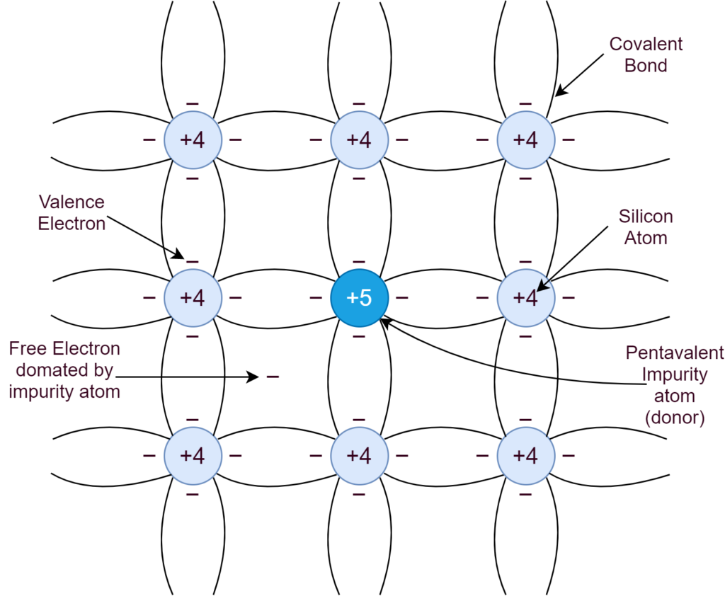
When the intrinsic Silicon is doped with an element, having five (5) valence electrons, the concentration of negative (n) charge carriers increases, and, as such, the semiconductor is called N-type. In the careful process of N-type doping, the Phosphorous shares four of its electrons with neighboring atoms of Silicon to form covalent bonds. Whilst, leaving behind a free electron and, in this way, each Phosphorous atom donates a free electron to the Silicon crystal. In N-type doping, Phosphorous is a donor element (donating electrons) and no holes are there. The majority of carriers are electrons.
Figure 4: N-type Silicon structure, Impurity (donor) with a bound positive charge.
The concentration of donor atoms is much greater than the concentration of thermally generated charge carriers. The major concentration of negative (N) charge carrier is due to doping and is independent of temperature. Whereas, the sole concentration of holes is due to thermal generation and can be calculated by the formula given above.
In the N-type semiconductor, the concentration of electrons (negative charge) is much higher and independent of temperature. So, electrons are majority carriers and holes are minority carriers in N-type semiconductor.
P-type Semiconductor
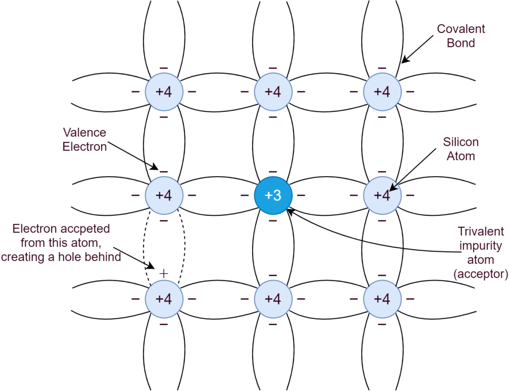
When the intrinsic semiconductor, such as Silicon, is doped with elements having three (3) valence electrons under a precisely controlled environment. The trivalent impurity atoms make four (4) covalent bonds by accepting electrons from the neighboring Silicon atoms. The Silicon atom donates electrons, here, and leaves behind a hole/ positive charge. The semiconductor, where Silicon atoms donate electrons to impurity and create positive ions, is P-type semiconductor. Now, holes/ positive charges are the majority carriers.
In a P-type semiconductor, the intrinsic semiconductor is doped with elements of Group-III e.g. Boron. The three (3) electrons of this trivalent Boron makes four (4) covalent bonds by accepting an electron from Silicon, as depicted in the following figure:
Figure 5: P-type Silicon structure, impurity(acceptor) with a bound negative charge.
The hole generated by adding impurity, attracts electrons from neighboring Silicon atoms and, effectively, makes a hole(s) shifting from one place to another and this process keeps repeating. Due to high impurity concentration, the holes are significantly high in numbers as compared to electron-hole pairs, generated due to thermal generation. This P-type doping makes holes/ positive charges as the majority carriers and electrons as the minority carriers. The majority carrier’s concentration is dependent on doping level and, whereas, the minority carrier is dependent on thermal generation.
It is eminent to mention here that a pure semiconductor material is neutral. In N-type semiconductors, the majority carriers (electrons) neutralize the bound positive charges of Phosphorus atoms. Similarly, in P-type semiconductor, the majority carriers (holes) neutralize the negative bound charges of Boron atoms.
Electric potential, when applied, causes the current flow in the semiconductor. In semiconductor two types of current flows: drift current that is due to drift of charge carriers; and diffusion current that is due to diffusion of charge carriers into less concentrated areas.
Conclusion
Intrinsic semiconductors have mobility carriers due to thermal generation only and they are minority carriers in doped semiconductors.
An impurity added to an intrinsic semiconductor makes it a doped semiconductor.
In doped semiconductors, the majority carriers are either electrons (N-type) or holes (P-type) and their concentrations are dependent on doping level.
Doping of intrinsic semiconductors with pentavalent impurity atoms makes electrons as majority carriers. A property of N-type semiconductor.
In N-type semiconductor, impurity is the donor of electrons and has a bound positive charge.
Doping of intrinsic semiconductors with trivalent impurity atoms makes holes as majority carriers. A property of P-type semiconductor.
In P-type semiconductor, impurity is the acceptor of an electron and has a bound negative charge.
Both N-type and P-type semiconductors are electrically neutral, as a whole.
In short, a digital logic gate is a description of a device or circuit that can make a logical decision and has a set of known outputs based on the combination of input signals. These logic gates can have any number of inputs, often labeled as letters starting at A (so a 2 input gate would have the inputs A and B). They also generally have one output, labeled wither Q or Y. These gates can also be combined to make much larger digital circuits, to create a desired function or behavior. These much larger systems can have any number of inputs and outputs and can have either combinational or sequential behavior (we will learn more about the difference later). Logic gates are also not always physical devices. Some devices such as FPGA’s use the logic of logic gates to describe the hardware created within it. Also in software, there are often logic functions that act in the same way but are just a description of the algorithm. Logic gates are all around us and are a key base of computer science.
fig 1: An integrated circuit or 8 pin microchip. image source: depositphotos.com
In this series of tutorials, we will focus on the physical logic chips that are widely available, and a useful resource for engineers starting out. There are two main families of logic chips widely available and accessible, the older CMOS series (Complementary Metal-Oxide-Silicon) which is known as the 4000 series of chips, and TTL (Transistor Transistor Logic) which is the more widely used 7400 series. Note that TTL and CMOS are purely the way the logic is functioned within the chip, and how the chip is fabricated in production. The chips often act in the same logical way, but aspects such as voltages, rise/fall times, and price can all vary between series and manufacturer. There are also other technologies, some older and some newer that produce logic, for instance, RTL (Resistor Transistor Logic) was the technology that ran part of the Saturn V rocket in the 60’s. There is also Diode Transistor Logic and Emitter Coupled Logic. All these components are housed within the chip that is then known as an IC (integrated circuit).
fig 2: Logic chips can come in many packages, but a popular breadboard-friendly variant is the DIP package shown above. These are 4000 series chips made by ST Microelectronics.
Integrated Circuit Classification
These integrated circuits can often be grouped into different levels of complexity. For instance, a simple XOR gate is much simpler than a modern GPU and has a vast difference in the amount of transistor circuitry involved. There is a common categorization of integrated circuits based on the size that can be used as:
Small Scale Integration (SSI) containing up to 10 transistors (AND, OR, NOT gates).
Medium Scale Integration (MSI) containing between 10 and 100 transistors (more complex combinational logic such as Adders, mux, and flip flops).
Large Scale Integration (LSI) between 100 and 1000 transistors (units using 100’s of logic gates, such as memory, ALU’s and I/O chips).
Very Large Scale Integration (VLSI) between 1000 and 10000 transistors (small processors, and programmable logic devices).
Super Large Scale Integration (SLSI) between 10000 and 100000 transistors (microprocessors, microcontrollers, some complex calculators)
Ultra Large Scale Integration (ULSI) 1,000,000+ transistors (FPGA’s, complex CPU’s, GPU’s and some high end microcontrollers).
There are also devices that go much higher, with devices like SoC’s, which can be as complex as an MPU inside a complex FPGA, and can be known to contain as many as 100 million individual transistors. In 1965 a co-founder of Intel, Gordon Moore came up with what is now known as Moore’s Law, where he predicted that the number of transistors/resistors in a chip will roughly double every 18 months, based on changing technologies. At the time, they were developing technology in the Medium Scale Integration classification, where you would find just over 50 transistors in a chip. The first-ever microprocessor, the 4004, had roughly 2,300 transistors (Large Scale Integration) in 1971. When compared to now, there can be over a billion transistors on a modern Processor.
Logic States
To understand how logic gates work, we first have to understand the rules. Basic digital logic gates perform different functions based on inputs, which we will learn if further tutorials, but they are all based around 2 states. One state is classed as logic HIGH, “1”, or TRUE, and the other state is logic LOW, “0”, or FALSE. Basically, a signal is either ON or OFF. Most of the maths for this was developed by a mathematician called George Boole, who created Boolean Algebra, which you may hear described often in computer science. In Boolean Algebra, you have the states “1” and “0”.
It can be slightly confusing when using some forms of digital logic, as traditionally most logic gates use what is referred to as positive logic, where a positive voltage is equated to a “1” or logic high, but some input/outputs of digital logic-based systems can use negative logic, where a positive voltage is seen as a “0” or logic low. A good example of this is a when an output of something is connected to the cathode of an LED, to turn the LED “ON” you need to set the output to logic “0” or ground. We will discuss this concept further in later tutorials.
Voltage Levels
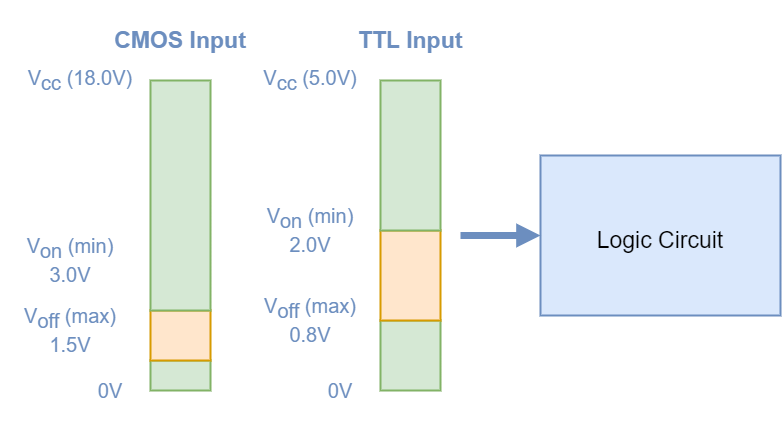
There are many different families of logic gates, and as discussed above, many different technologies get used. Each family within the technology will also have it’s own voltage range that can be accommodated by the inputs to produce that “0” and “1” signal. By in large, TTL is fairly simple with regards to what constitutes a signal. A voltage between 2.0V and 5.0V is a logic high and a voltage between 0V and 0.8V is considered logic low. This is assuming that a +5V rail is used as the power supply, if it is lower, then the upper end of the logic high is reduced to the supply voltage.
Due to the technology of CMOS devices using FET’s rather than bipolar transistors, CMOS uses slightly different logic levels. A logic high is classed as between 3.0V and 18.0V, and a logic low is below 1.5V. Similarly to the TTL voltage levels, the upper limit is reduced with a lower supply voltage. In essence, a logic low should be as close to ground as possible, and a logic high can comfortably be 5V in either technology, with 3.3V operation also being comfortable in TTL based systems. CMOS systems could run on 3.3V, but it would likely be too close to the 3.0V switch, to make a stable circuit.
fig 3: The standard inputs to a CMOS and TTL logic gate
Digital Noise
Now the digital voltage levels have been clearly defined, we notice there is a clear voltage range in between where a signal can be too high to be “0” but too low to be a “1”. This is useful to stop signals switching erratically during operation, but on occasion, this gap is not actually big enough. This is where noise becomes a real problem, but what is the noise we care about? A signal in a circuit is very rarely a stable voltage, and even if it seems stable, the closer you look, the less stable it appears. Noise is the name given to a random voltage interference on a signal, usually caused by other parts of a circuit, or nearby circuits. Circuits such as power supplies, or fast switching modules can cause electromagnetic radiation, which can cause a spike (where signal goes very high) or a trough (where a signal goes low). If you have an input that is low, and you have a spike, it could read as an input high for a split second, which makes the circuit function incorrectly. There a number of methods that can be adopted including de-bouncing circuits, and Schmitt triggers, but that will be covered in future articles.
The 7400 Family of Devices
As discussed above, the 74 family of logic gates is a very powerful, and widely used TTL bipolar transistor-based family of devices. It is often easy to notice these devices, with it often having a 74 prefix. For instance, a 7400 device is a Quad 2-input NAND gate, and a 7432 is a quad input OR gate. These families go into the hundreds of different circuits, and there are long lists in places such as Wikipedia outlining the general sequence. These devices also come in a number of different sub-families, which define the voltages, speeds and often price of that device. These can be recognized in the letters between the 74 and the device number. Below is a quick list to reference some of the popular subfamilies of 74 logic.
74xx or 74Nxx: The standard basic TTL.
The original devices, introduced in the 70’s.
Propagation delay of 10ns.
Power consumption of 10mW.
Supply voltage range of 4.75V to 5.25V
74Lxx: The low power TTL.
Designed to improve power consumption.
Slower switching, but less power.
Supply voltage range of 4.75V to 5.25V
74Hxx: The high-speed TTL.
Designed for faster switching speeds.
Faster switching, but more power.
Supply voltage range of 4.75V to 5.25V
74Sxx: The Schottky TTL.
Using Schottky technology.
Lower impedance, higher switching speed, lower power consumption (~2mW).
Supply voltage range of 4.75V to 5.25V.
74LSxx: The low power Schottky TTL.
Designed to improve power consumption of Schottky TTL.
Supply voltage range of 4.75V to 5.25V.
74ASxx: The Advanced Schottky TTL.
Improving the switching of Schottky TTL.
Much higher switching speeds, but much higher power consumption (~22mW).
Supply voltage range of 4.5V to 5.5V.
74ALSxx: The advanced low power Schottky TTL.
Improved the previous Schottky TTL devices.
low power consumption (~1mW), and high switching speeds (4nS).
Supply voltage range of 4.5V to 5.5V.
74HCxx: The High Speed CMOS.
A very popular form of the 74 family.
Reduced power consumption, and CMOS compatible inputs.
Supply voltage range of 4.5V to 5.5V
74HCTxx: The High Speed CMOS.
Designed to reduce power and but lower speed to 16nS.
Still has TTL inputs.
Supply voltage range of 4.75V to 5.25V
The 4000 Family of Devices
As with the 74 family of devices, the 4000 series has a common numbering system generally across its families that can be used to remember what they do. They are known for the 40 prefix. CMOS devices can be popular due to their high speed and low power applications, which is why they are employed in some later 74 devices, but the main disadvantage is their susceptibility to ESD (static electricity), also the supply voltage range can be a limitation on occasion rather than a benefit. With modern electronics going to increasingly low voltages to improve switching speeds and power consumption, the 4000 series is seen less and less, and being accumulated into other families. The two common sub-families are:
4000B Series: The standard CMOS.
Original buffered logic, introduced in the 70’s.
Supply voltage of +3V to +18V.
74C Series: 5v CMOS.
Compatible pinout to the 5V TTL devices.
Has TTL compatible inputs and outputs.
Still operate from 3V to 18V.
Conclusion
In conclusion, digital logic gates are highly useful devices that can be used to create much larger circuitry, based on just a few rules. We also learnt about the different physical device families, and some of the implications and considerations needed when choosing the devices to use. This has given us the basis to start learning about the individual logic gates going forward.
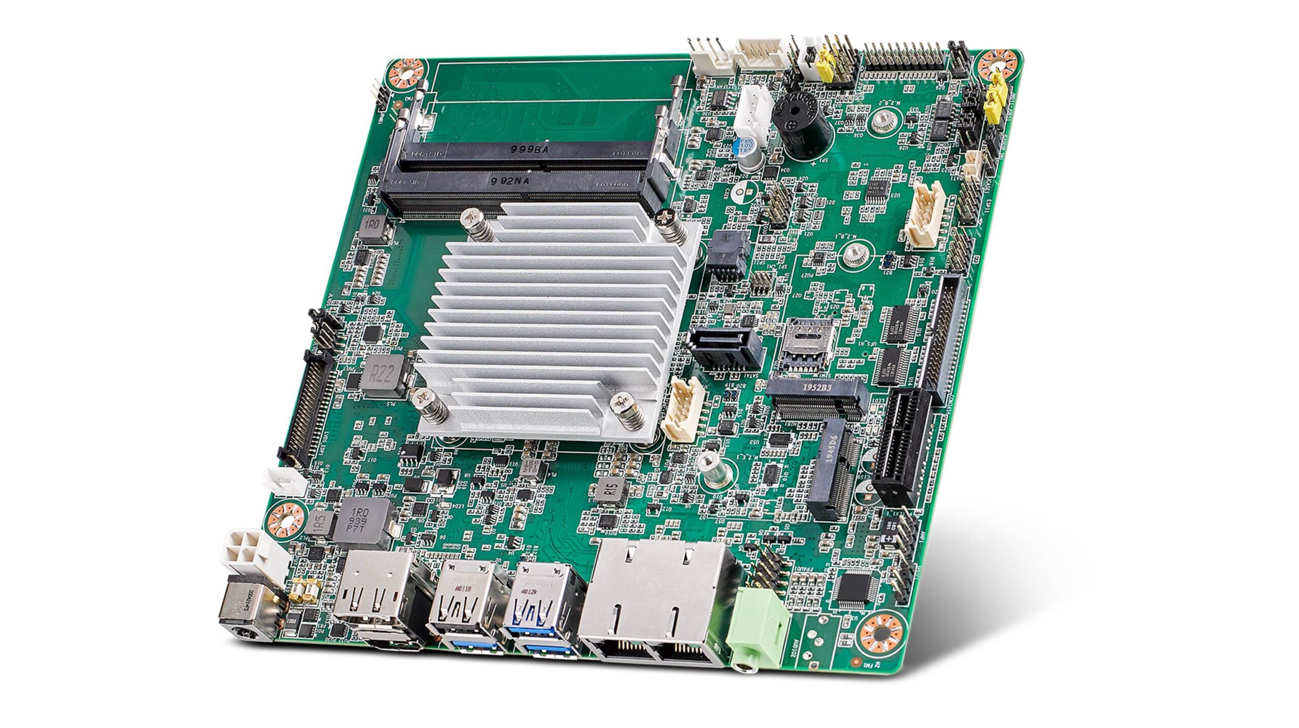
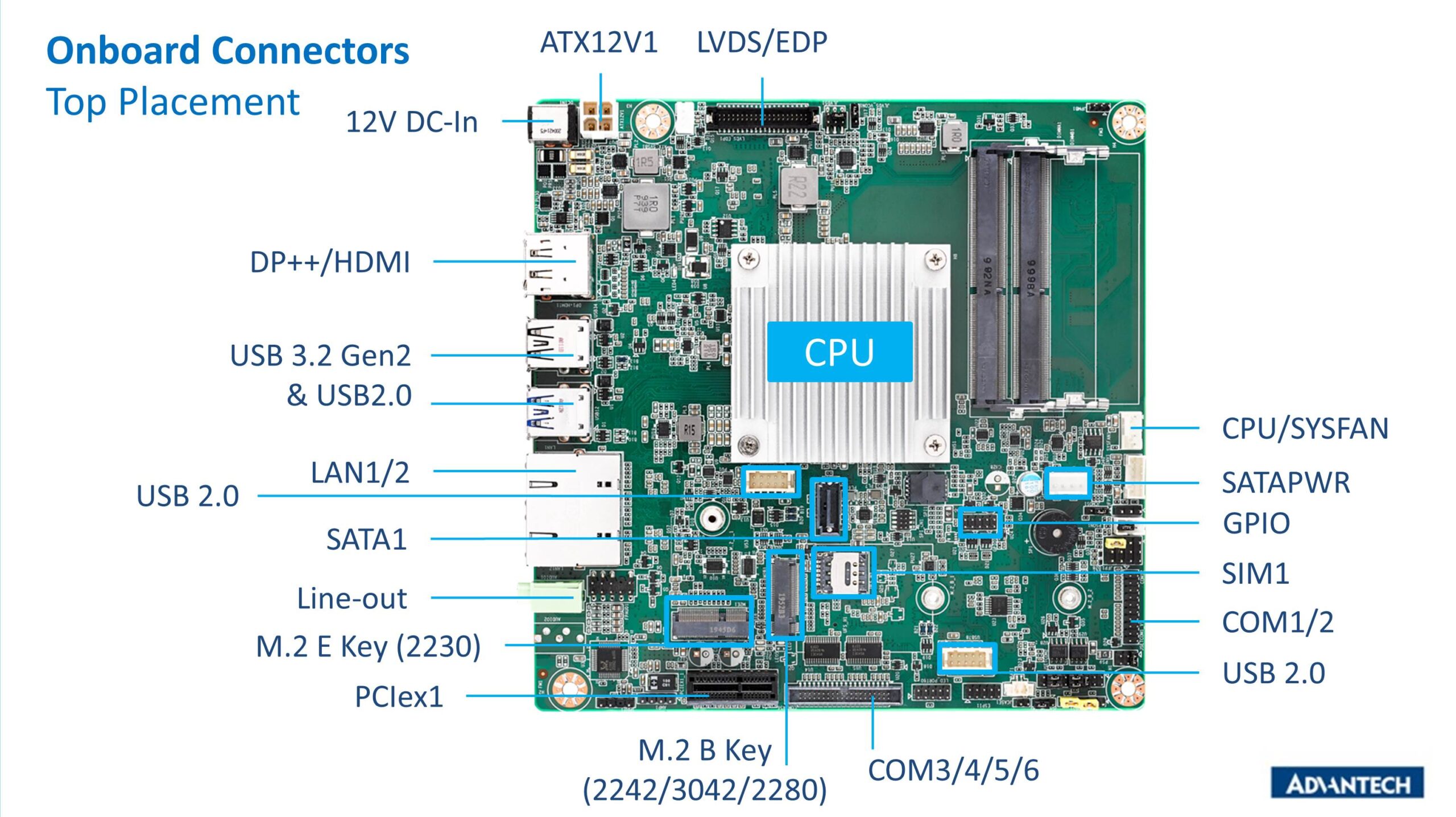
Advantech, a global leader in embedded IoT solutions, is pleased to release AIMB-218, a low-profile fanless industrial-grade Mini-ITX motherboard featuring Intel Atom® x6000E, Intel® Pentium®, and Celeron® N and J Series processors. Based on low-power 10nm technology (6 ~ 12W TDP), AIMB-218 supports up to 4 cores with 3.0GHz turbo frequency and up to 850MHz of Gen 11 Graphics, yielding a 50% improvement in CPU performance, and doubling its graphics processing capabilities. AIMB-218 is designed for industrial edge computing applications that require high-resolution graphics and reduced energy consumption — including applications in smart kiosks, digital signage, industrial controls, and medical devices. Additionally, its wide operating temperature (-20 ~ 70 °C /-4 ~ 158 °F) is adaptable to semi-outdoor industrial environments.
Intel® UHD Graphics and UFS 2.0 Deliver Ultra HD Video Playback
Advatech’s AIMB-218 delivers superior graphics capabilities via Intel® UHD Graphics up to 32EUs. AIMB-218 supports rich display interfaces — including DisplayPort 1.2, HDMI 1.4, LVDS, and eDP; delivering 4K resolution progressive scan at 60 fps on 3x displays. Additionally, AIMB-218 features an improved memory capacity via DDR4 3200MHz up to 32GB with IBECC. This solution supports innovative onboard UFS 2.0 with 32 ~ 256GB storage to increase transfer rates to 1200 MB/s — twice as fast as SATA III. AIMB-218 achieves low latency for high-resolution video content in embedded display control applications by using its next-gen. graphics, high-speed memory, storage, and data transfer rate capabilities.
Flexible High-Performance in a Compact Design
AIMB-218’s practical small form-factor design (height of 21 mm/.82 in) features diverse I/O, including dual GbE LAN ports, 3x USB 3.2 Gen2, 5x USB 2.0, and 1x SATA III. Moreover, AIMB-218 supports 6x high-speed capable (1Mbps) COM (COM 1 supports 5V/12V, COM2 supports RS-232/422/485 auto-flow control) to improve data synchronization precision over the network and reduce latency during device communication.
Advantech’s AIMB-218 offers 1x PCIe Gen. 3 to improve AI capabilities. Its 1x M.2 (E key) for Wi-Fi and Bluetooth module, and 1x M.2 (B Key) with SIM card holder for LTE and SATA modules support efficient scalable networks and storage configurations. All of the expansions are placed on the top of the device for easy flexible modular expansion.
AIMB-218L/J/D (Intel® Pentium® and Celeron® N and J Series) and AIMB-218Z (Intel Atom® x6000E Series) will be available in the first quarter of 2021. Samples are now available! Please contact Advantech or visit https://www.advantech.com/ to find out more.
AIMB-218 Key Features:
Intel® Pentium/Celeron/Atom® CPU
Dual channel DDR4-3200 260-pin SODIMM up to 32 GB with IBECC*
Supports 3x displays via HDMI1.4b, DisplayPort1.2, and LVDS (or eDP)
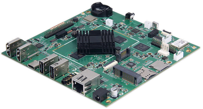
Geniatech’s RK3568 development board is a slight update in its RK3566 board. The RK3568 board comes with an Arm Cortex-A55 core and a Mali-G52 GPU for power graphical processing. Both the boards are the latest AIoT boards from Rockchip, but the RK3568 features some extra I/O ports in respect to RK3566.
The RK3568 as well RK3566 development boards are equipped with its industrial-grade motherboard for stable continuous operation. VPU features video decoding with 4Kp60 H.264 and H.265 capacity and video encoding with 1080p60 H.264 and H.265 capacity. The camera I/F comes with 8M ISP with high-dynamic-range imaging. RK3568 and RK3566 both consist of MIPI CSI2 functioning at 2.5 Gbps per lane and digital video port camera support with BT.656/601/1120.
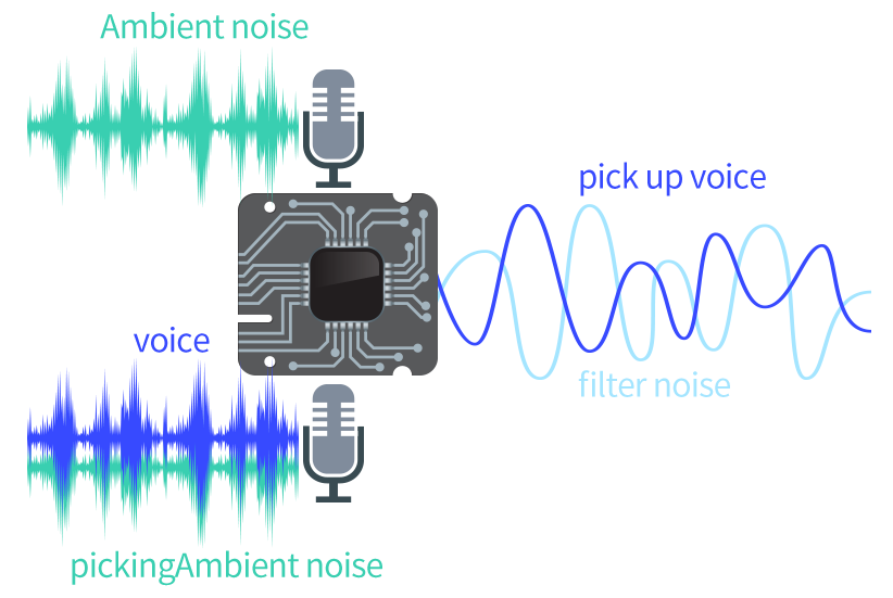
The RK3568 development board comes with voice noise reduction technology with a 2-way microphone and double MIC matrix for noise reduction and sound detection to be more efficient. One of the microphones picks up the voice including the ambient noise, whereas the second mic far from the user just picks the ambient noise. Hence, the ambient noise from the second mic is used to reduce the noise picked from the first mic. This allows significant noise reduction.
Technical Specifications of RK3568 Development Board
Mali-G52 GPU and 0.8-TOPS NPU
Storage of 4GB LPDDR4 and Up to 128GB eMMC 5.1
MicroSD slot up to 512GB up to 2 slots
802.11a/b/g/n/ac with Bluetooth 5.0 technology
RF tuner input featuring ATSC
GTIoT interface for Z-Wave, ZigBee, LoRa, GPS, WiFi, BT 5.0, or LTE
Pair of antenna mounts
Ports for HDMI 2.1 out port, HDMI in port, and eDP 1.3
Dual-channel and 24-bit LVDS through MIPI-DSI
Dual mic matrix with noise reduction
SPDIF audio and 4-lane MIPI-CSI
Scalable using M.2 slot with PCIe 3.0 and wireless storage support
Power rating of 12V/2A input jack
Operating system supporting Android 11 or Linux
CNX Software’s post has brought to our attention that both the boards are almost similar with the same specifications and functionalities, except for the processors. However, the RK3568 development board comes with triple display support and PCIe 3.0, while the latter supports a lower dual display and PCIe 2.1. USB-C port may also feature USB 3.0 OTG functionality for the RK3568 development board while the RK3566 board only supports the USB 2.0 OTG feature.
The RK3568 development board is compatible with a hard disk interface allowing customer data reading and writing functionality. It also features larger storage space and quicker transmission speed. The applications for the RK3566 and RK3568 development boards include AI robots, face recognition, smart POS machine, and some smart home applications. The operating system for the development boards supports Android 11.0 and Linux’s Buildroot, Debian, or Yocto.
There is no pricing information available on Geniatech’s website, but there is a section for “Volume Quote” for both the development boards.
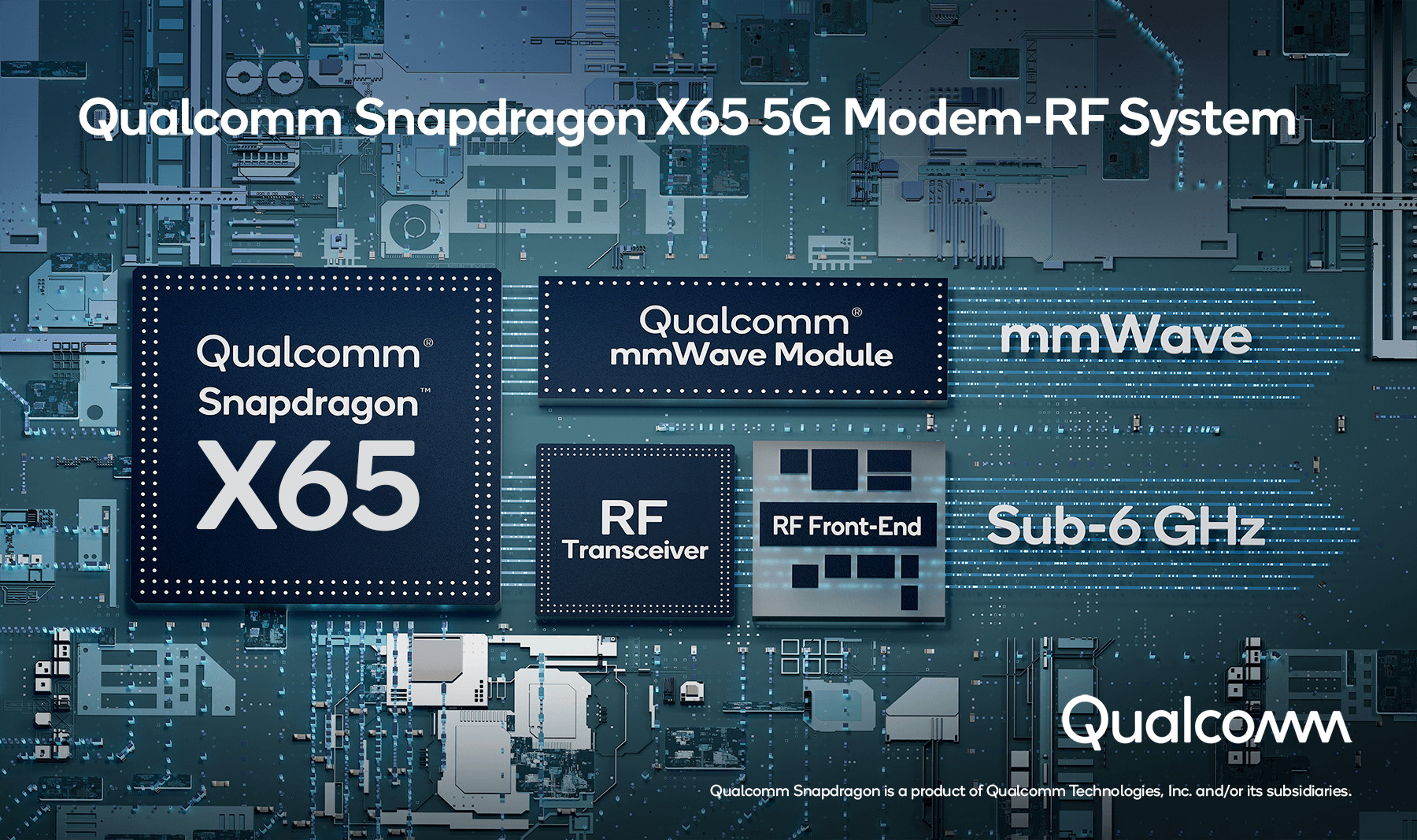
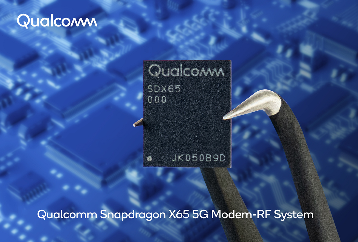
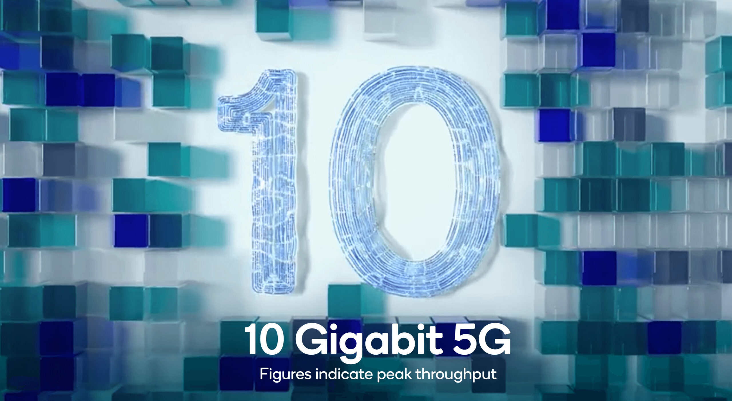
When it comes to the system on the chip in your smartphone, tablet, or even the wireless modem, Qualcomm has dominated the market for quite a few years now. A few days back, the company announced World’s first 10 gigabit 5G modem-RF system that will increase the 5G support in mobile broadband, compute, XR, industrial IoT, 5G private networks, and fixed wireless access. This becomes the fourth generation Qualcomm Snapdragon X65 getting the first 3GPP release with 16 modem-to-antenna solution.
The manufacturer added more to its announcement with the release of the SnapdragonX62 5G Modem-RF system, a modem-to-antenna solution designed for mainstream adoption of mobile broadband applications. The X65 5G Modem-RF system is designed with an upgradable architecture that allows the adoption of new features while reducing the total cost of ownership. Qualcomm showcases the QTM545 fourth-generation mmWave antenna module that increases the mobile mmWave coverage area and improves power efficiency.
The innovation does not stop here, the X65 also has the world’s first AI antenna tuning technology that has enhanced the tuning capabilities leading to faster data speeds, better coverage, and longer battery life. When it comes to power saving, Qualcomm has also been at the forefront. To add to this, X65 gets Qualcomm’s 5G PowerSave 2.0 that comes with new power-saving technologies defined in 3GPP Release 16.
“The 5G transition presents the biggest opportunity for Qualcomm as mobile technology is poised to benefit virtually every industry,” said Cristiano Amon, president and CEO-elect, Qualcomm Incorporated. “We are reaching a significant milestone with the Snapdragon X65 5G Modem-RF System, unleashing connectivity up to 10 Gigabits per second and support for the latest 5G specifications that will play a critical role in enabling new 5G use cases not only for redefined premium smartphone experiences, but also opening a new realm of possibilities for 5G expansion across mobile broadband, compute, XR, industrial IoT, 5G private networks and fixed wireless access.”
If you are still wondering ‘why’ it is important and significant to launch the product in the broader aspect of the industry. With the release of 10 Gigabit 5G, it is necessary to have a 5G Modem-RF System that will bring a new set of features to premium smartphones. The company explains by saying:
“With multi-gigabit 5G enabled by the Snapdragon X65 5G Modem-RF System, consumers will have access to fiber-like browsing speeds and low-latency, delivered wirelessly over 5G for the next generation of connected applications and experiences, including cloud- and edge-based computing, highly responsive multiplayer gaming, rich entertainment, immersive 360-degree video, and instant apps.”
For those interested in the products, Snapdragon X65 and Snapdragon X62 are expected in the commercial devices by late 2021.
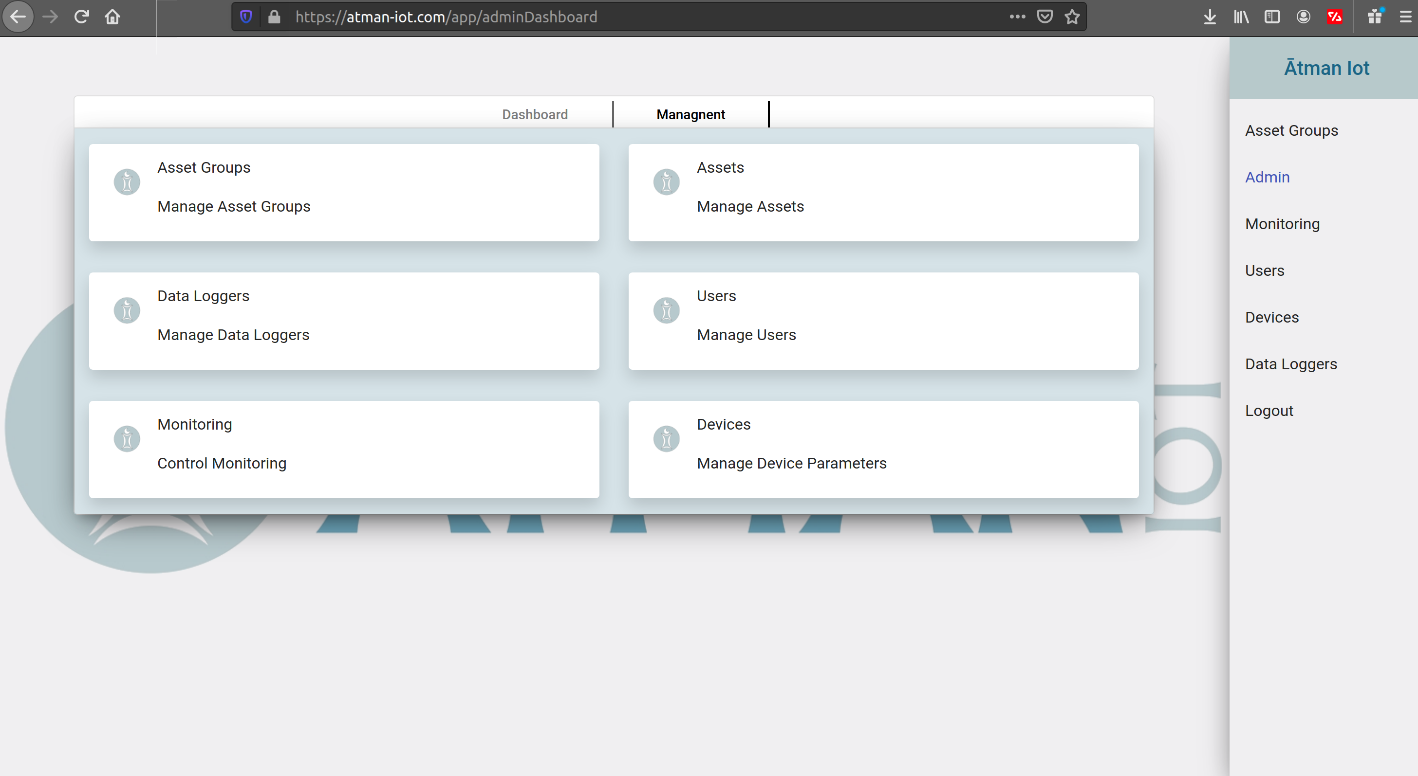
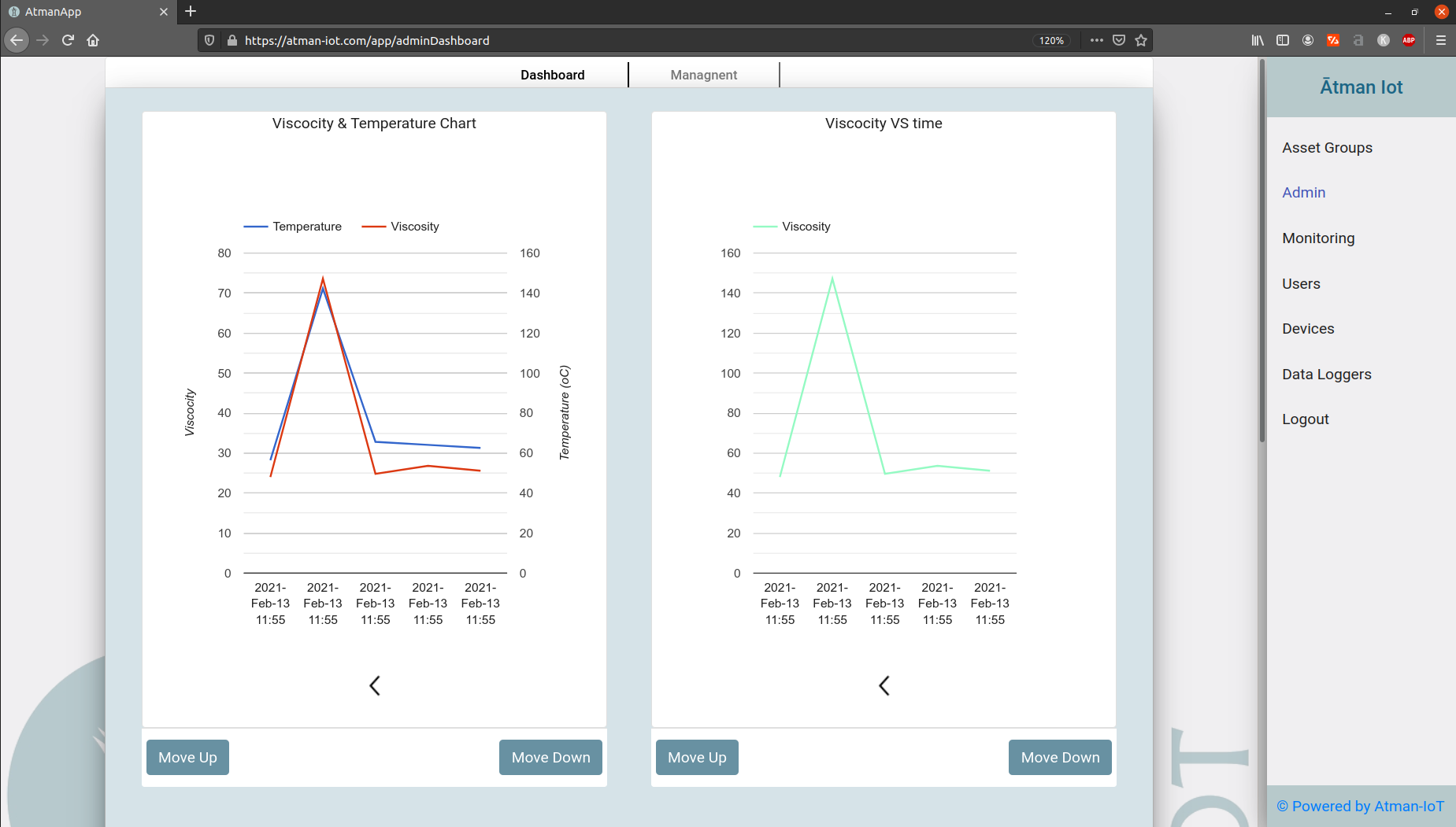
Atman IoT Platform as a Service (PaaS) is the ideal solution for getting your IoT solution up and running in a very short time. Atman IoT is also available as a stand-alone server, packaged in a preconfigured, ready to use Docker container.
Atman IoT Platform is a Service, focused on rapid IoT solution prototyping. Its focus is to help IoT solution developers get their product out with as little effort as possible. For that reason, it offers a responsive OEM web app that can be customized to the project’s and client’s needs. It can be downloaded and installed on any web server and the rest is handled in the background.
For developers that want to build their apps on top of Atman IoT, it offers an extensive API with open source connector libraries in a number of client and server frameworks, and programming languages, including Angular, RXJS, NodeJS, Python, Go, PHP Laravel, and more.
For more demanding applications, Atman IoT if offered also as a stand-alone server packaged as a ready-to-use docker container, available via docker hub.
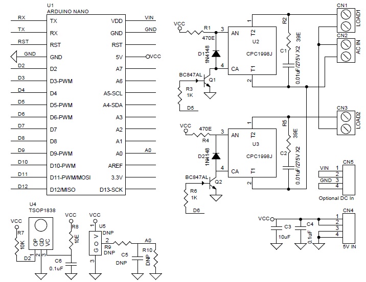
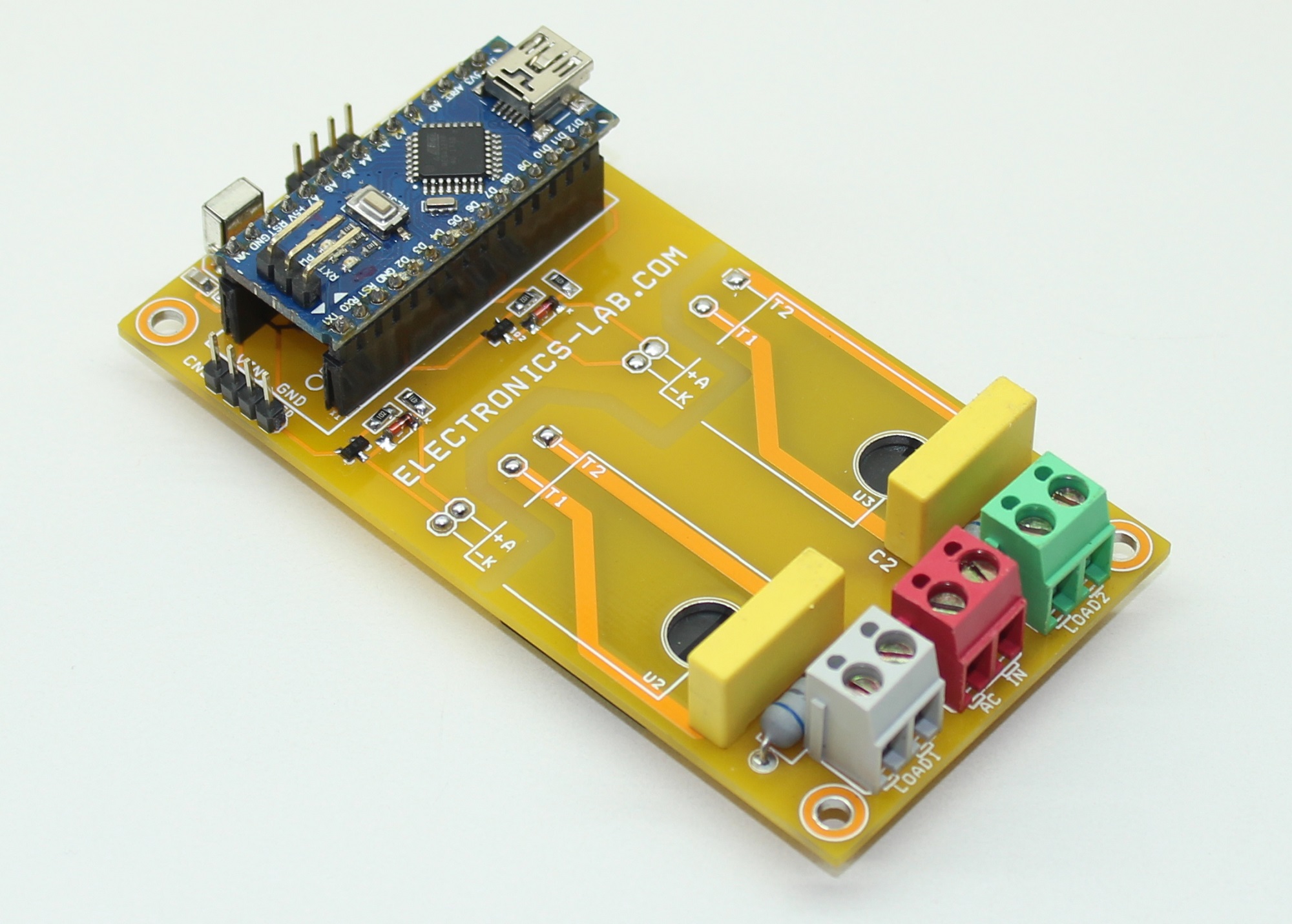
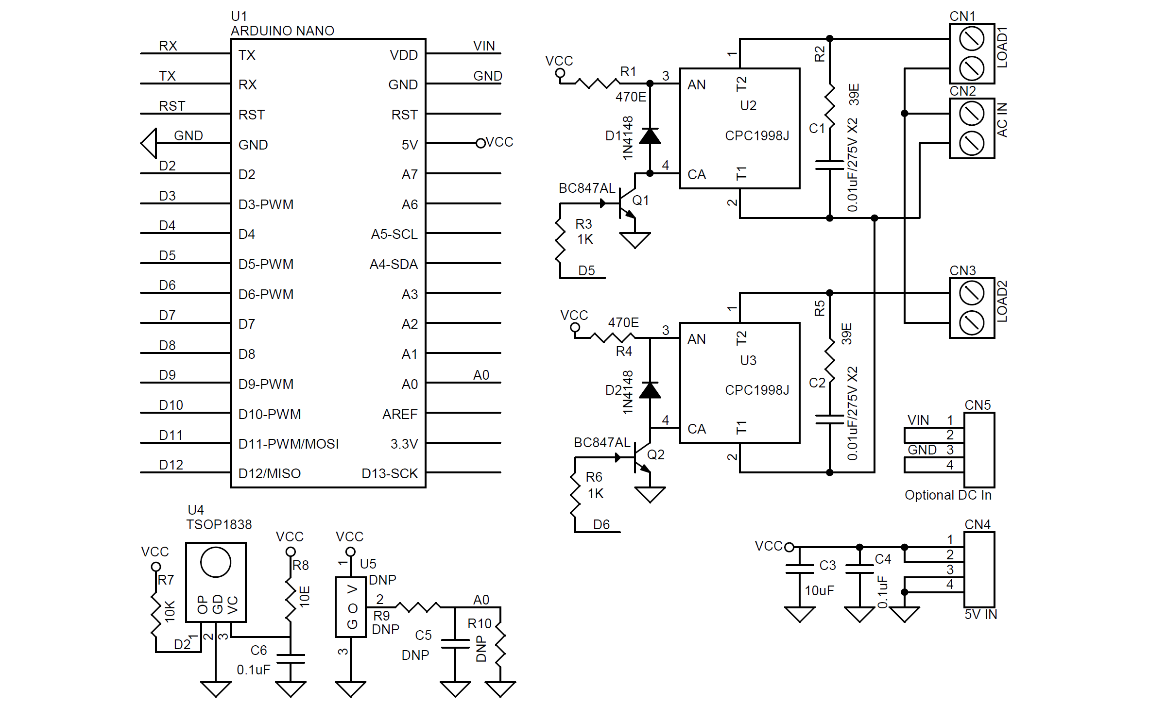
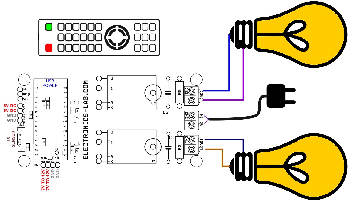
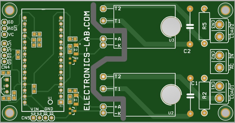
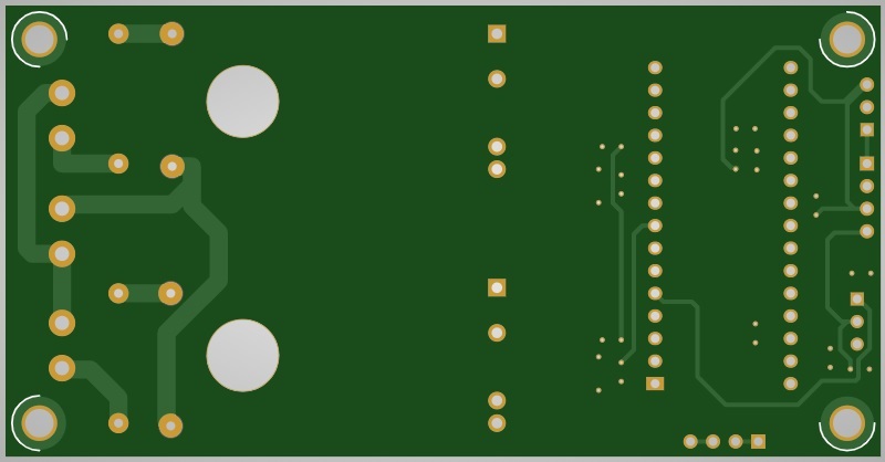
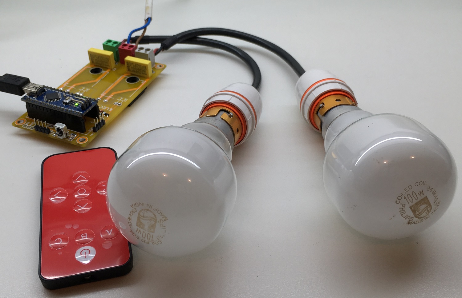
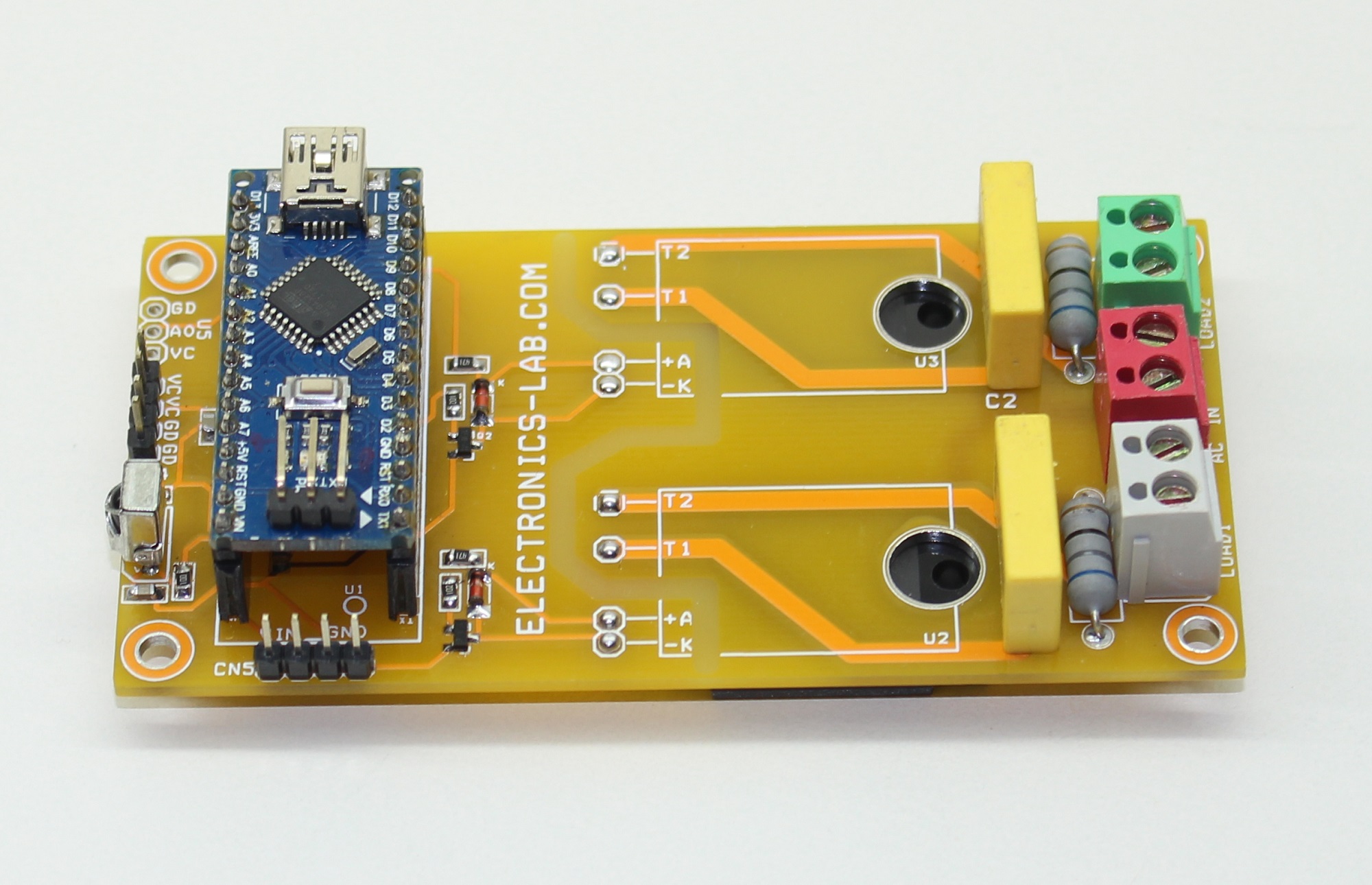
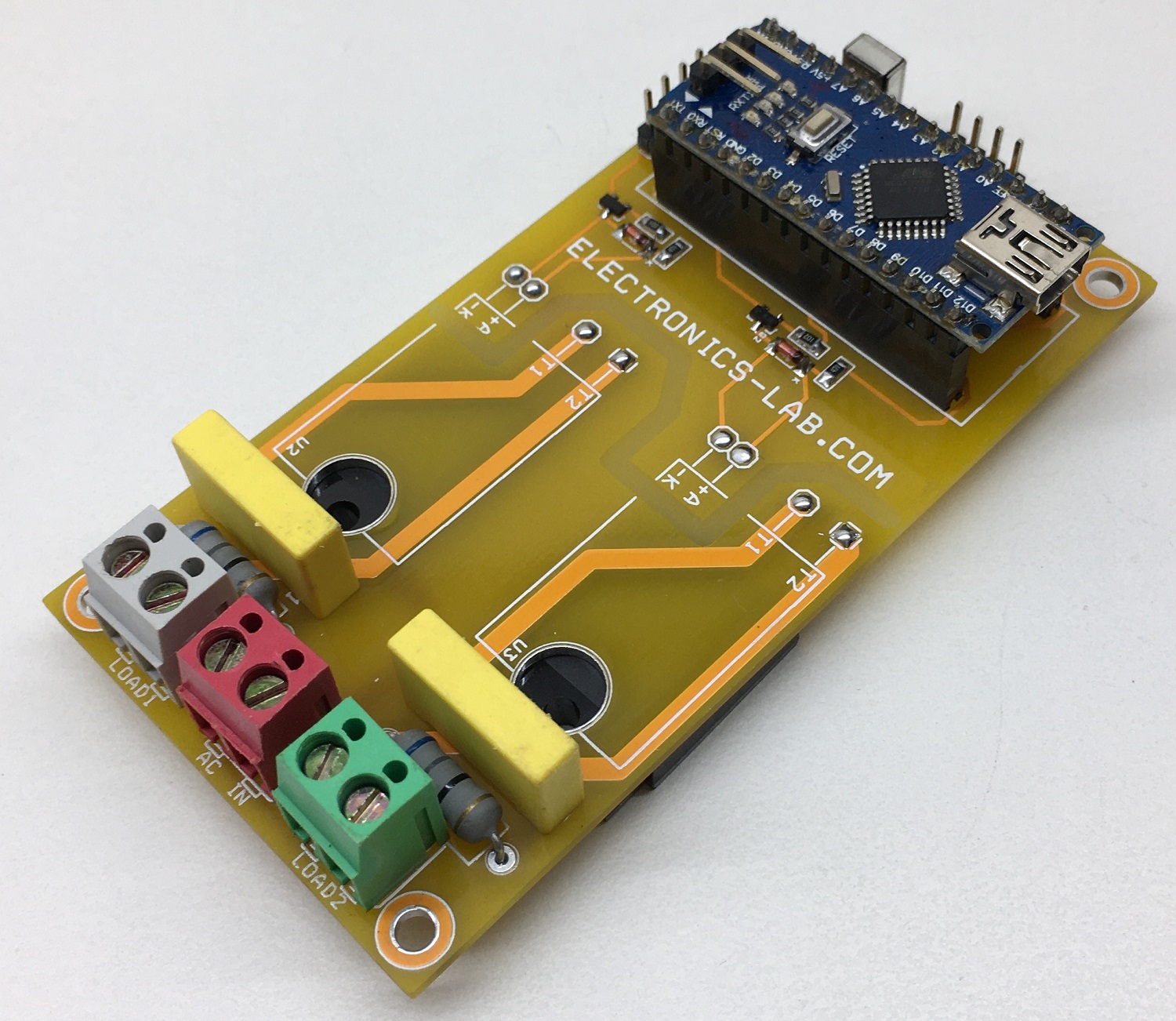
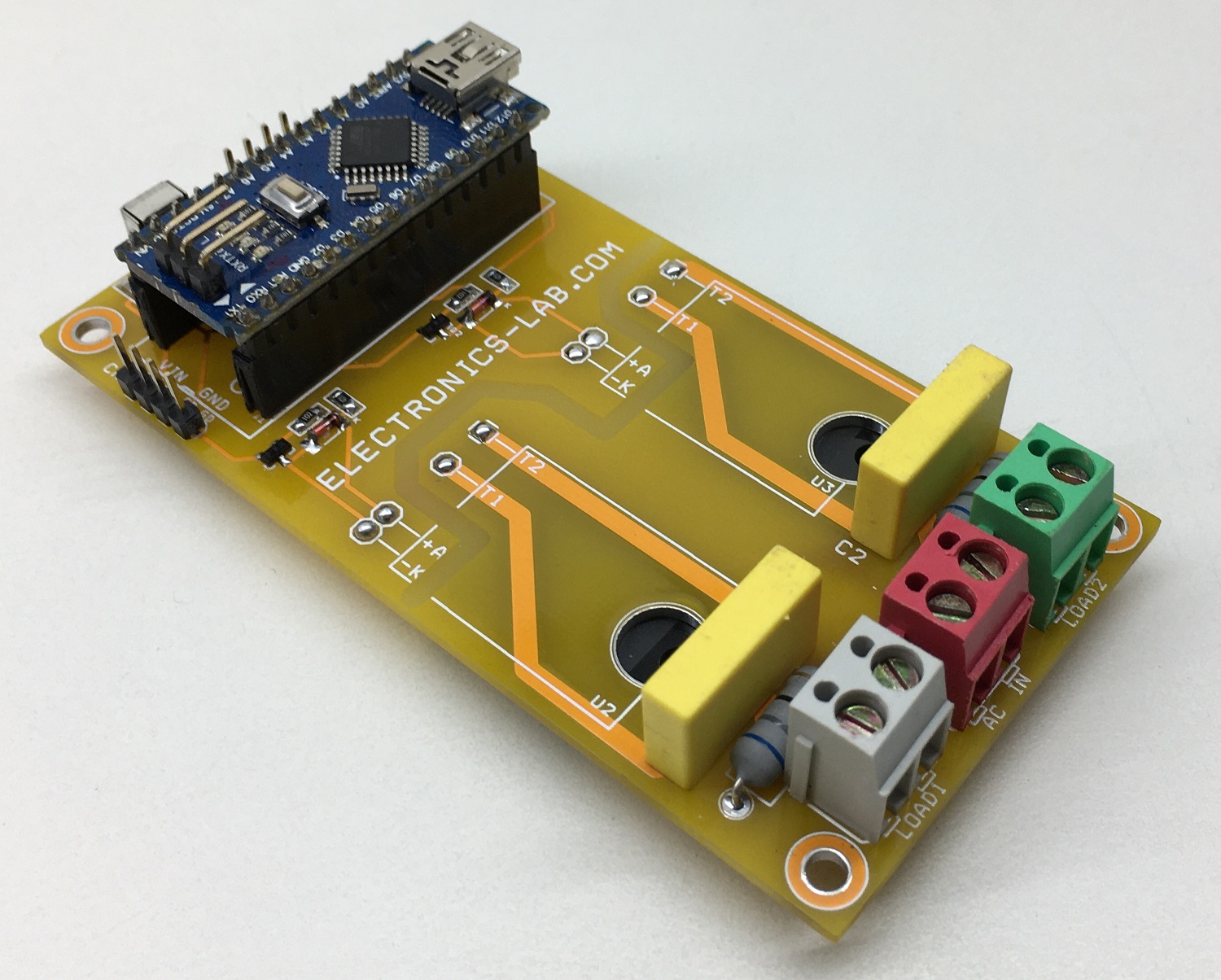
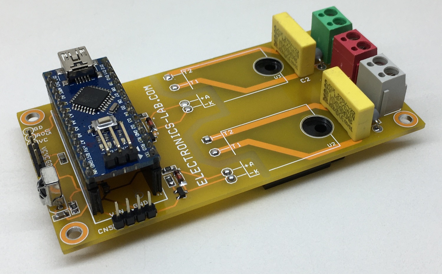
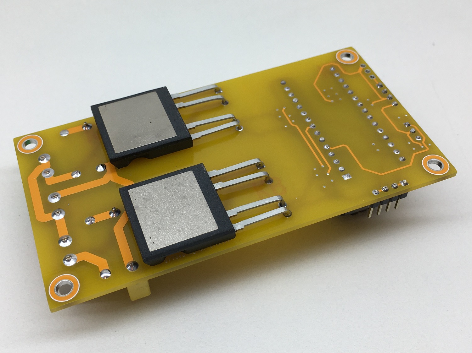
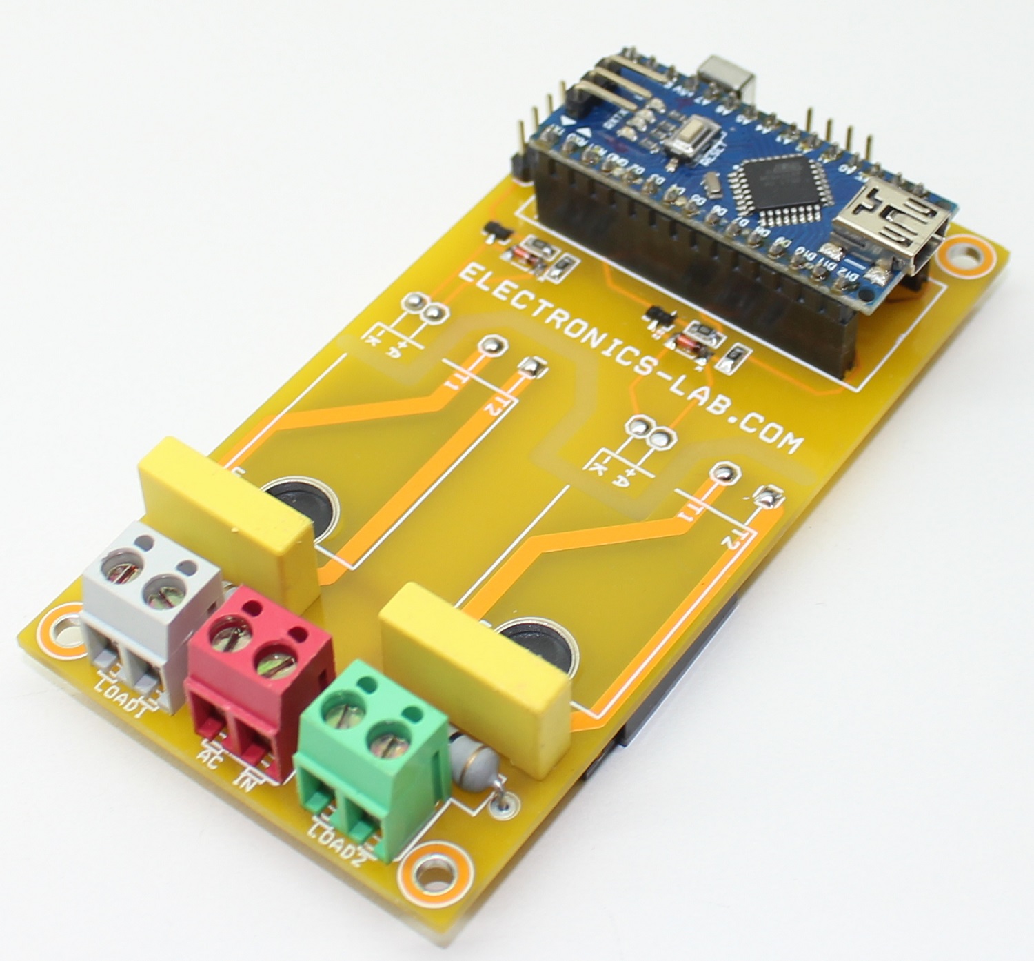
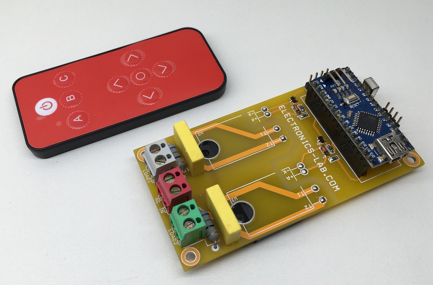
The project presented here is a two-channel infrared remote ON/OFF switch that can be used to control home appliances, Lights, Fans, Water Pumps, Aquarium pumps, Ovens, Heaters, etc. This open-source project contains 2 x SSR (Solid State Relay), Arduino Nano, and TSOP1838 infrared receiver, keeping safety in mind, optically isolated SSR (Solid State Relay) is used to have isolation between high voltage AC circuitry and Arduino Nano. The operation of the circuit is pretty simple, TSOP1838/TSOP38238 IR Sensor receives the infrared signal from IR remote, Arduino Nano decodes the IR signal which is connected to digital pin D2 and provides latch outputs on digital pins D5, and D6 in respect to IR code received from IR remote. These two digital outputs D5, D6 drive the SSR using 2 x BC847 BJT transistors. CPC1998J optically isolated solid-state relays from IXYS Integrated Circuits drive the AC loads. We have tested this board with 500W/230V AC lamps, however, the load capacity of SSR is 20A. A snubber circuit is provided across the SSR-Traic which helps driving inductive loads. Heat-sink on SSR is not required for loads up to 5A, but for higher load, it is advisable to mount a heatsink on SSR.
Components Functions: U2 & U3 SSR Relay AC Load driver, U4 TSOP1838/TSOP38238 IR Sensor, R1 & R4 Current limiting resistor for SSR LED, Q1 & Q2 LED Driver of SSR, D1 & D2 Protection Diode for SSR LED, C1 & C2 + R1 & R5 Snubber Circuit for AC Inductive Load.
Connections: CN2 AC Input 110V-220V AC, CN1 Load, CN3 Load, CN4 5V DC Supply If Arduino Nano USB power is not available, CN5 DC Power (Optional) 7V to 12V if USB/5V power is not available.
Power Supply DC: The Arduino Nano can be powered via the Mini-B USB connection, 7-12V unregulated external power supply (CN5), or 5V regulated external power supply (CN4).
CPC1998J is an AC Solid State Switch utilizing dual power SCR outputs. This device also includes zero-cross turn-on circuitry and is specified with an 800VP blocking voltage. Tightly controlled zero-cross circuitry ensures low noise switching of AC loads by minimizing the generation of transients. The optically coupled input and output circuits provide exceptional noise immunity and 2500Vrms of isolation between the control and the output. As a result, the CPC1998J is well suited for industrial environments where electromagnetic interference would disrupt the operation of plant facility communications and control systems
Arduino Pin configurations: Digital Pin D2 TSOP1838 Infra-Red Receiver, Digital Pin D5 and D5 outputs
Note 1: This board can accommodate other SSR like S216S02 from Sharp, CPC1998J from IXYS or KSD215AC3 available from http://www.cosmo-ic.com
Note 2: This project also can be used for many other applications that require 2 x SSR, Optional U5 connector is provided to interface analog/digital device or sensor
Code
Arduino Example code is provided to test the project, code is compatible and paired for SparkFun Remote Model COM-14865, Switch A and Switch C defined for Load1 and Load2, more info on the remote is available here.