4D Imaging RoC Sensor: Interview with Vayyar’s Head of Automotive

Vayyar's RoC Sensor Board

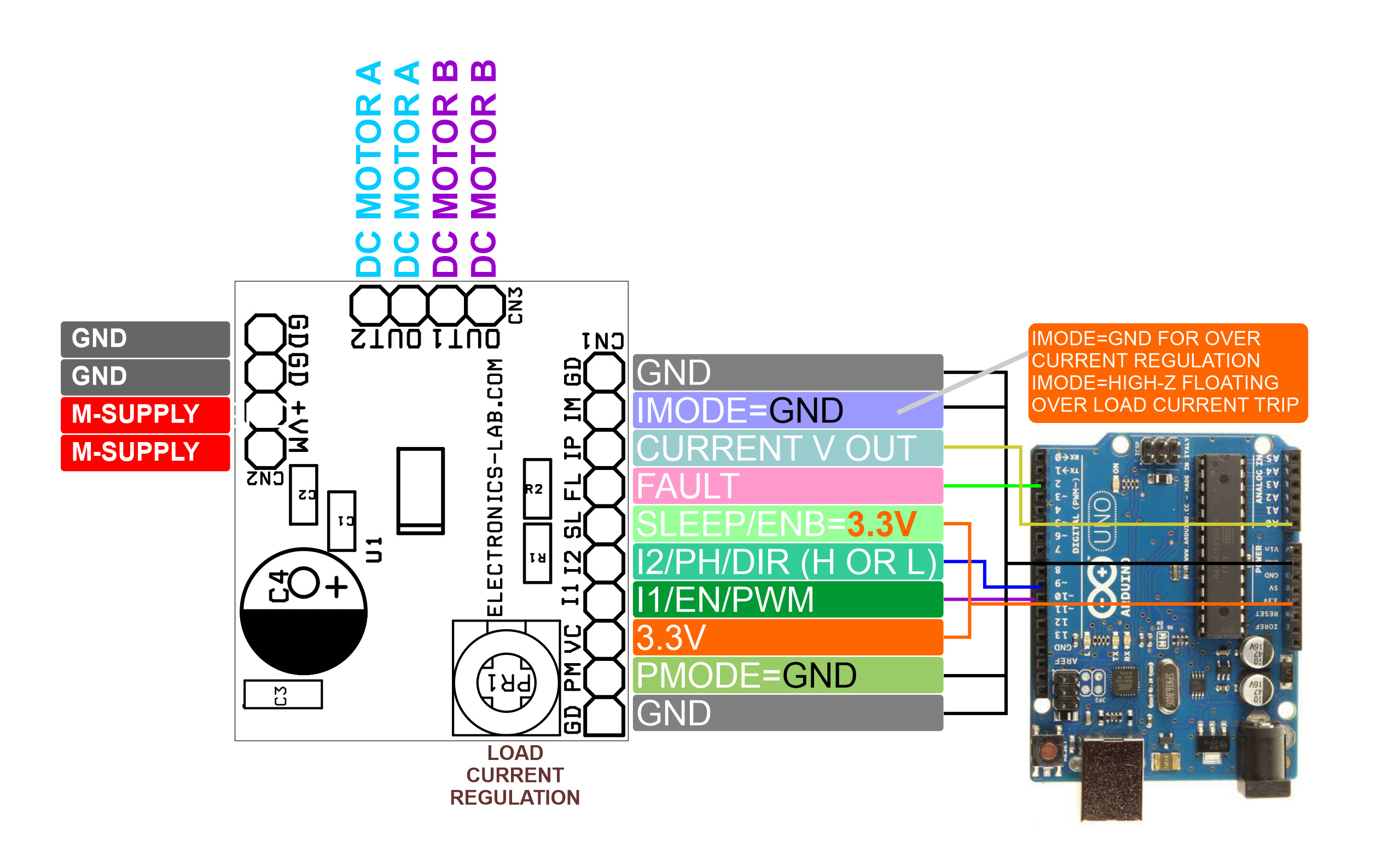
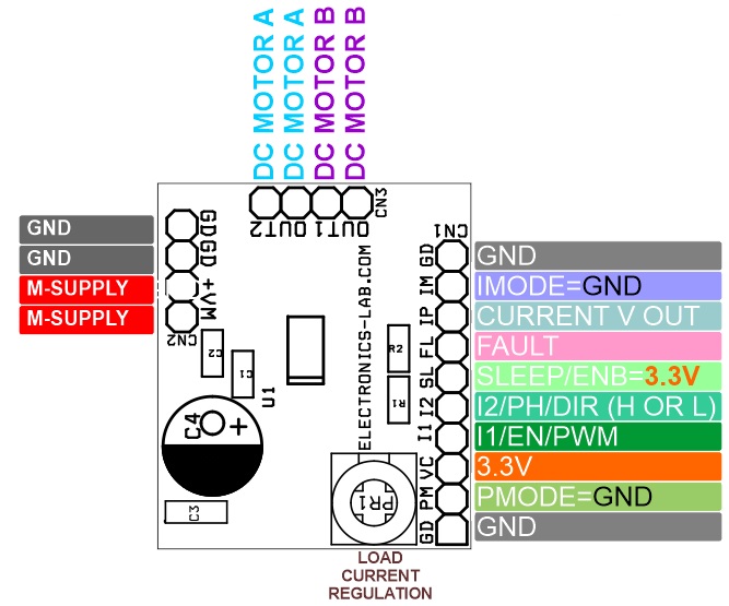
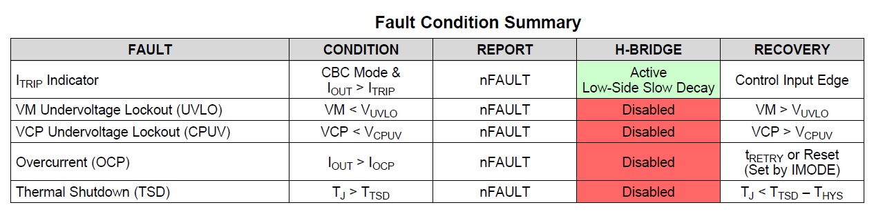
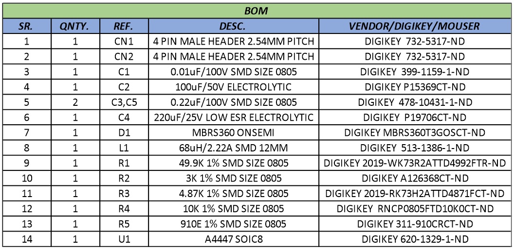
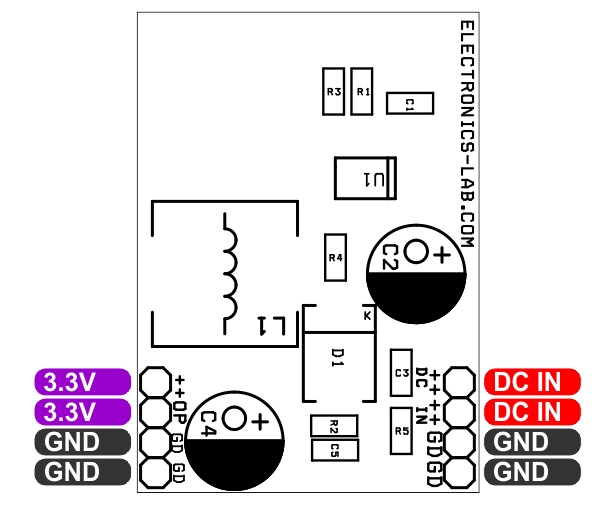
The 4D imaging technology using cameras and LIDAR comes with drawbacks as the cameras are sensitive to external environmental conditions like bad light, fog, etc. Hence, the radar technology for 4D imaging allows a good resolution scan with an accurate field of view. Vayyar’s Radar on Chip (RoC) is one such example for 4D Imaging applications.

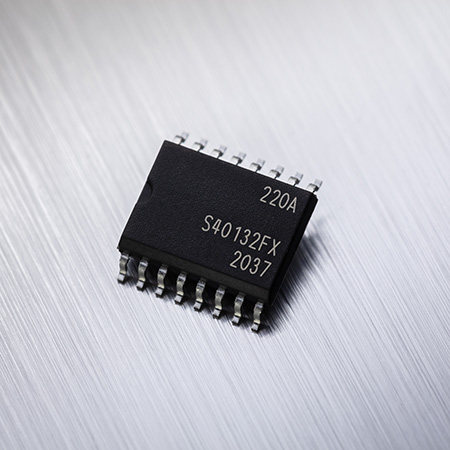
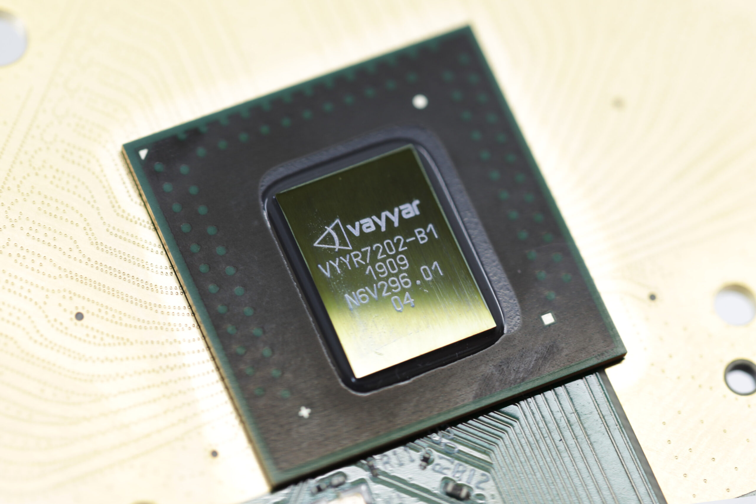
The automotive-grade RoC is AEC-Q100 approved and is equipped with up to 48 transceivers in the mmWave range. It also features a digital signal processor (DSP) and a microcontroller unit (MCU) for real-time signal processing. The 4D Imaging RoC replaces the requirement of many antennas at different locations and fits everything on a single chip. This improves the form factor and reduces the overall cost.

The 4D Imaging RoC supports many features including intruder alerts, Child Presence Detection, enhanced Seat Belt Reminders, and eCall to alert emergency services in the event of a crash. It also features posture detection by imaging at a good resolution of around 5cm pixel, hence it allows analysis of the pattern in pixels for prediction of posture.

4D Imaging RoC

The 4D Imaging RoC replaces the overall strength of multiple chips by sensing, computing, processing, mapping, and imaging targets by compacting everything on a single RoC. The sensor is designed dynamically for scalability, flexible for the deployment of emerging features through over-the-air (OTA) software updates.

For information on Vayyar’s 4D imaging RoC technology visit the announcement and the company website.

Interview with Vayyar’s Head of Automotive

I also got an opportunity to interview Ian Podkamien, Head of Automotive of Vayyar Imaging. The interview has all the possible questions that a tech enthusiast like me can have. Here is the transcript of the complete interview:

Saumitra: What is the basic principle that the sensor follows for 4D Imaging? Is it the conventional way where the rays are passed in a particular space, and the obstruction in the frequency or path of the ray detects the object for imaging?

Ian: The principle is as you said, you have a transmitting antenna that will send the radio wave which will propagate, bounce, and then propagate back to the receiving antenna. This is the very old traditional radar style, for calculating the direction and the distance of that object. What we do is something very different which is called Imaging Radar instead of transmitting directional beam and measuring distance and direction. We use many antennas, the more number of antennas we include the better is the resolution. A single antenna transmitting will cover about 180 degrees and the arena under the antenna will start reflecting back on the receiving antennas. Hence, using multiple transmitting and receiving antennas improves the granular resolution of imaging radar and increases the field of view significantly.

Saumitra: If you could give a number, how many antennas are there on the chip?

Ian: The Vayyar chip has around 72 antennas, 24 antennas in the ultra-wideband domain, and 48 antennas in the mmWave. It would be dependent on the geo applications, hence we provide multiple frequencies for implementing multiple applications according to the regulations.

4D Imaging in Automotives

4D Imaging in Automotive

Saumitra: Do you have any cloud server on which the computations and processing take place, or everything happens on the sensor itself?

Ian: That is a good question and probably I have a good answer for it. The philosophy here is to be an enabler by developing on the high-resolution data, and to have a small form factor at a very low cost. This allows multiple flexibilities, one of them is having multiple bands (frequencies), and the other is that we have embedded all necessary computing power required, inside the single chip. The processing includes transceiving analysis of the antenna, data crunching, 3D re-constructions, and 4D re-constructions.

Also, post-processing which is application and level-based complex computing, everything happens on the chip. The chip also features transporting data to 3D point cloud API  to the embedded ARM for embedded applications development, as well as exporting the point cloud outside the sensors for places where there is a need for fusion. Fusion with a camera is a very basic example of this. So, if you want to have your computations on the chip itself or you want to use the sensor for fusion with other devices, both are possible with Vayyar’s chip.
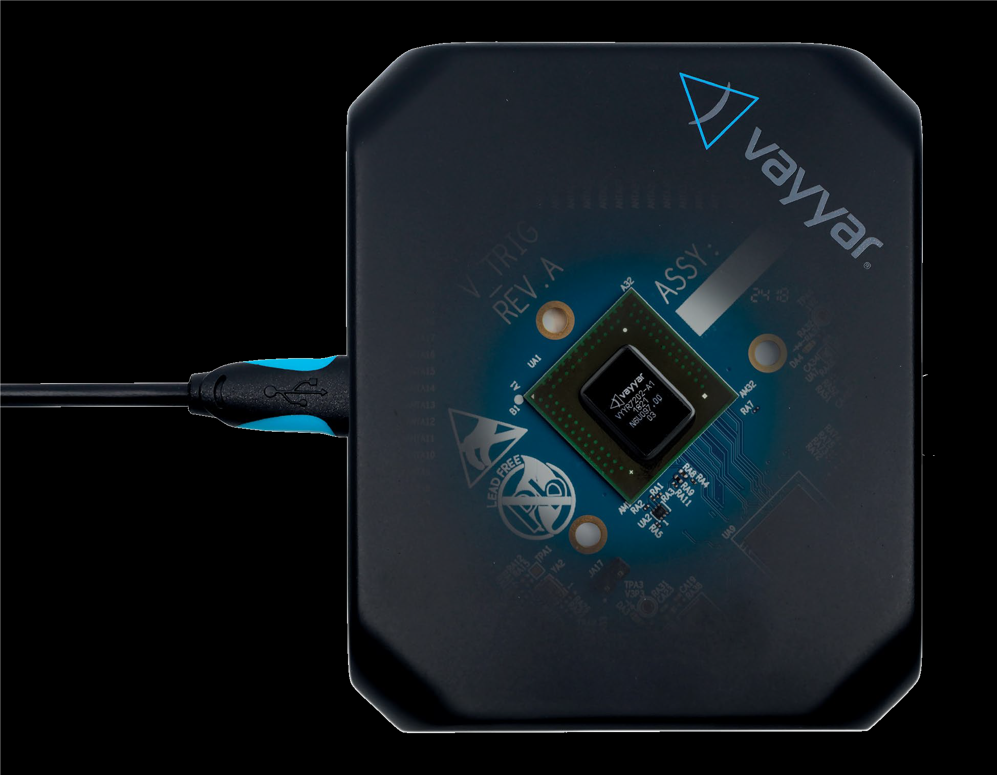
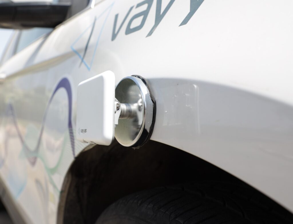
Deployed RoC Sensor

Deployed Application of RoC

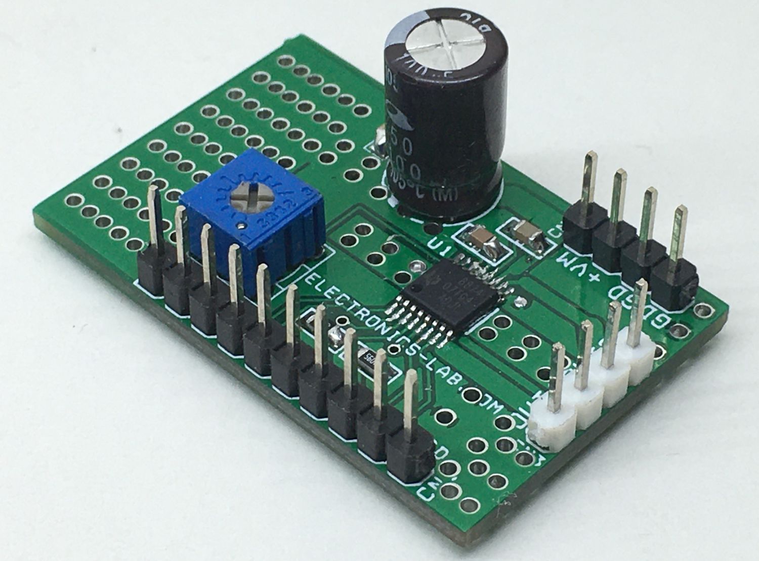
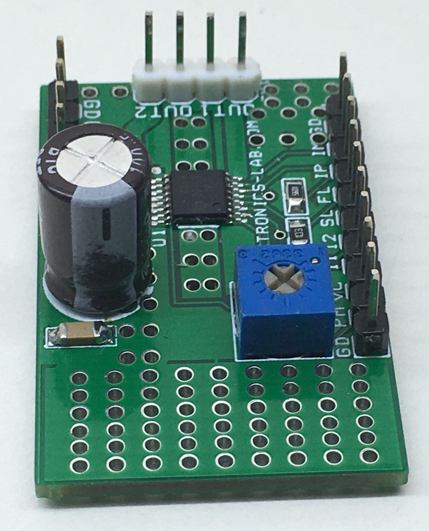
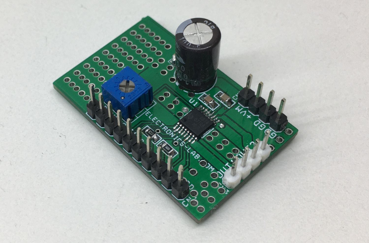
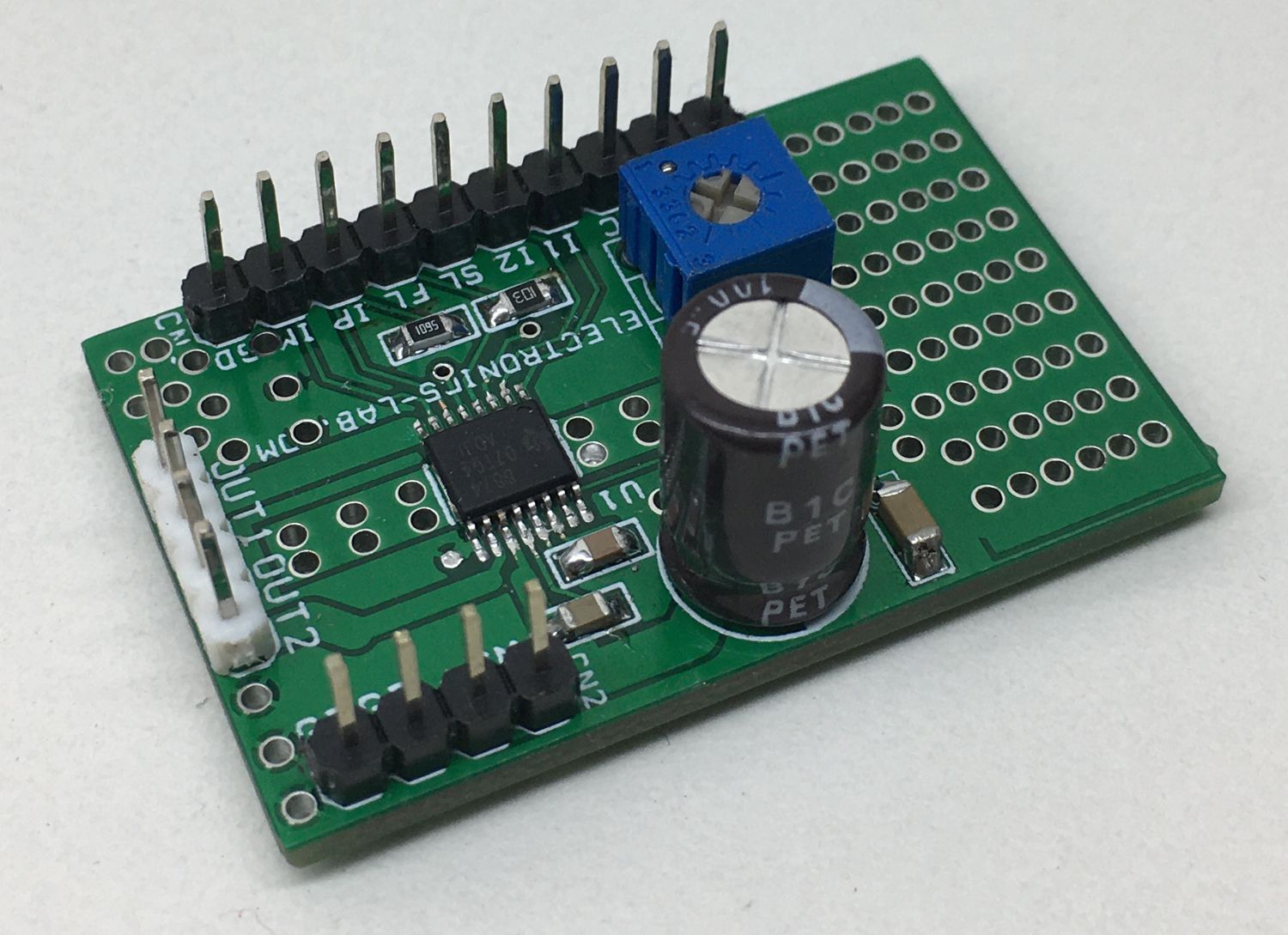
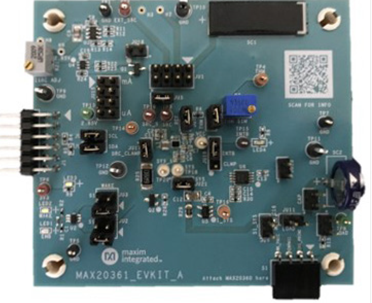
Saumitra: Do you plan on launching a development board of Vayyar that could be great for personal use? For adding some customized features depending on the user applications?

Ian: We have several of those, ranging from professional and more  expensive development kits for companies to low-cost development boards for independent users. Vayyar has its own consumer brand called Walabot. It actually has two major products, one is a Walabot wall scanner device that is capable of “seeing” up to 4 inches inside the wall. Also, we have a development kit which is called Walabot Maker that comes with 20 antennas. This costs about a few hundred dollars. It is not very different from a Raspberry Pi, you can connect it to a PC. It comes with a developer SDK and a bunch of sample codes for reference.

Saumitra: Talking more about the Walabot Maker. Where is it available and do you plan to release more products like these?

Ian: Well, it is available on the Walabot website and we have been selling it for quite a long time with successful results. I can tell you that we are now ramping onto a more sophisticated innovation kit that would be launching soon. It will be available online in various locations. The device will have more than 40 antennas in mmWave.

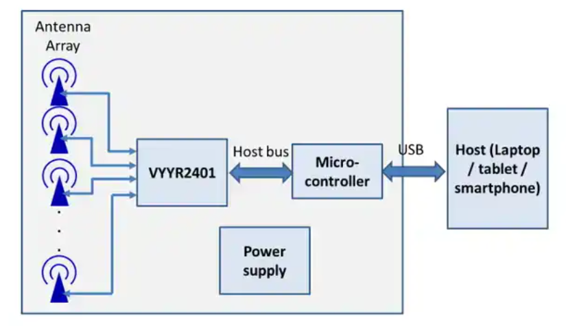
Walabot Maker’s Block Diagram

Walabot Maker's Block Diagram

Saumitra: What is the operating system that powers the device? Adding to this question, Is your software open source? As the readers are more curious about the software being open source as it supports the device with community support.

Ian: No, the inner software of the chip is our secret sauce in a closed environment but, the API is really a powerful one that enables creating your own dataset. If there is a group of people who want to create a dataset over the same API then it can have great community support. But, the hardcore algorithms are our secret sauce.

Saumitra: What is the power rating of the device, if you could give a number?

Ian: It is a very low-power device, it is less than a phone charger. It is plugged in with a USB for power supply for consumer versions. For embedded solutions, we have a constant DC power supply. If I have to give a number, it can go from 5 W to 10 W depending on the applications with a very low power mode for stby and power save.

Saumitra: Apart from the automotive industry do you plan to expand your device’s application in imaging? For example in military or medical or any industry that requires 4D imaging?

Ian: Actually it is the opposite, we started the company with a medical device for breast cancer. Instead of Mammography, we have a portable device like a bra. Within 10 seconds you have full 3D imaging of the breast with WiFi equivalent frequencies. The device is not at all painful and comes at a low cost. I believe it is a game-changer as it can allow many women to make prescreening on-time and frequently. We took the same imaging capability and expanded it to smart homes, robotics, and homeland security.

Snapdragon 888 Mobile HDK runs Android 11 on Qualcomm’s latest 5nm SoC

Qualcomm and Lantronix have come together to launch Snapdragon 888 Mobile Hardware Development Kit – a feature-rich Android development platform designed to provide Android app developers, hardware vendors, and original equipment manufacturers with the right software and tools needed to accelerate the development and testing of devices.

The Snapdragon 888 development board is powered by Qualcomm’s Snapdragon 888 octa-core Kryo 680 CPU with 1x Cortex-X1 core, 3x Cortex-A78 cores, and 4x Cortex-A55 cores, an Adreno 660 GPU, an Hexagon 780 DSP and a Snapdragon X60 5G modem. The processor is the latest premium mobile SoC from Qualcomm and it claims to have 25% faster CPU performance, 35% faster graphics rendering, 3x performance-per-watt improvement and 16x larger shared AI memory compared to its previous generation.

The Snapdragon 888 Dev board can be used to create a variety of high-end devices like smart-phones and tablets, mobile PCs, IP cameras, and artificial Intelligence gateways.

Features and Specifications of the development board include:

  • CPU: Qualcomm Snapdragon 888 (SM8350) Qualcomm Kryo 680 with:
    • 1x Cortex-X1 core running at 2.84 GHz
    • 3x Cortex-A78 cores running at 2.42 GHz, and,
    • 4x Cortex-A55 cores running at 1.80 GHz
  • GPU: Adreno 660 with support for OpenCL 2.0 FP, OpenGL ES 3.2, Vulkan 1.1, DX12, and up to 8K 360 VR video playback
  • Hexagon 780 DSP capable of 26 trillion operations per second (TOPS).
  • 12GB LPDDR-3200
  • 256GB of UFS 3.0 flash
  • 1x MicroSD port
  • Up to 4K DSI-driven HDMI 2.0 port
  • DisplayPort 1.4 via USB 3.1 Type-C
  • 3.5mm audio jack
  • 2x 4-lane MIPI DSI display ports
  • 6x 4-lane MIPI CSI with 3D camera support
  • Optional 6.65″ AMOLED touch screen with 2340 x 1080 resolution
  • Optional rear camera daughter card with 16MP + 48MP + 13MP camera, VGA ToF sensor
  • Optional front-facing camera accessory board with 20MP IMX476 front camera, MTT016 ToF camera
  • 1x GbE port
  • 802.11a/b/g/n/ac/ax WiFi 6 @ 2.4/5GHz; Wi-Fi 6E-ready
  • Bluetooth 5.1
  • 1x USB 3.1 Type-C port
  • 2x USB 3.0 host ports
  • 1x micro USB 2.0 port for debugging
  • 2x M.2 slots
  • Low-speed and high-speed I/O connectors
  • 2x sensors expansion connectors
  • Power Button
  • Volume button
  • 12V/5V power supply via power barrel jack
  • DIMENSIONS: 100 mm x 85 mm
  • OPERATING SYSTEM: Android 11

The Snapdragon 888 HDK by default ships with the Snapdragon 888 mainboard, a quick starter guide, 12V AC power adapter, USB cable and other optional accessories like a display expansion board, a rear-facing camera board and a front-facing camera board.

The complete kit is estimated to cost around $2,600 because the board itself is sold for $1,349, while the display board, the sensor board, and the rear-facing and front-facing camera boards are all sold for $499, $150, $299 and $299 respectively.


Further details on the HDK can be found in the following links:

IDS-310AI mini-PC with Apollo Lake SoC and dual Myriad X VPUs

IDS-310-AI mini-PCIEI’s IDS-310AI mini-PC for AI-enabled digital signage includes Apollo Lake SoC and supports 128GB SATADOM. It comes with a built-in Mustang-MPCIE-MX2 AI accelerator card, that includes two Intel Myriad X VPUs to provide a dynamic AI inference solution. It also functions to drive three displays through its 3x HDMI.

Talking more about the VPUs, the vision processing units can allow quicker deep learning computations which reduce the time in modeling. Also, the VPUs feature low power consumption applications such as “surveillance, retail, and transportation.” The power efficiency and performance allow Deep Neural Networks (DNN) topologies, that form the base of AI.

IDS-310AI has flexible connectivity with two Gigabit Ethernet RJ-45 ports through a PCIe GbE controller. It also features an optional M.2 module and external antenna. For expansion, the device comes with its M.2 2230 A-key slot and a mini PCIe slot fitted with an AI accelerator card.

Technical Specifications of IDS-310 mini-PC

  • Intel Celeron J3455 quad-core processor working up to 1.5GHz / 2.3GHz Turbo
  • System Memory includes 1 x 204-pin DDR3L SO-DIMM
  • 128GB SATADOM and MicroSD card slot for memory storage
  • 3x HDMI 1.4b ports up to 3840×2160 working at 30Hz each
  • 1x Mic-in and 1x Line out for audio functionalities
  • 1x RS-232/422/485 DB-9 with AFC
  • TPM 2.0 secure crypto-processor
  • Extruded aluminum alloy chassis with dimensions 137 x 102.8 x 49.2 mm

Ports of IDS-310AI mini-PC

The IDS-310AI fanless mini-PC is compatible with Linux or Windows 10 on a quad-core, 1.5GHz/2.3GHz Celeron J3455 with around 10W of total power dissipation. It also supports the Intel Open source toolkit Open Visual Inference Neural Network Optimization (OpenVINO). This allows AI acceleration for a large number of neural networks. The OpenVINO toolkit supports CNN (Convolutional Neural Network) and pre-trained models for on-device applications. The training models include AlexNet, GoogleNet, Tiny Yolo, Squeezenet, and resNet.

The working temperature range of the device ranges from 20°C to 45°C with airflow. The recommended rating of humidity has a large range from 10% to 95%, provided it is non-condensing. The power supply includes a 12V DC through a screw jack, with low consumption of 2.6A at 12V for an Intel Celeron J3455 with 8GB memory.

The low consumption feature makes the device a great option for implementing AI edge computing solutions by providing longer duty time for the rechargeable edge computing equipment. There is no information regarding the pricing or availability at this point in time. For more information visit the ICP Germany’s announcement and the product page on the IEI website. Images and technical specifications have also been taken from the product page.

H-Bridge Motor Driver with Integrated Current Sense and Regulation using DRV8874

In past, we have published many brushed dc motor driver boards for various projects and usually, they have some sort of limitations, as some of them are large in size, require large size heatsink, doesn’t have current feedback, they don’t have overload protection, some require external large size current shunt resistor and after all, recently we have found the amazing DRV8874 chip from Texas instruments that has some amazing features and protections features. It has a small package and can handle high current without a heatsink. We quickly become fans of this chip, and after a few tests and experiments, we are sharing this open-source module. This chip can be used with PWM/DIR input, PWM input, and 2 x Half-Bridge for dual motor control. We have tested this project with PWM/DIR inputs, and all inputs and outputs of the chip are accessible using the header connector. Refer to the datasheet of DRV8874 to explore other features and configure the board as per requirement. Example Arduino code is provided below.

Highlights

  • Speed Control
  • Direction Control
  • Current Regulation/sense
  • Over Current Trip

Features

  • Motor Power Supply 4.5V to 24V (Maximum Input 37V DC)
  • Load Current 0.5A/1A (3.7A Maximum)
  • Peak Load Current 6 Amps
  • PWM Frequency 10Khz to 20Khz
  • PWM Duty Cycle 0-100%
  • Proportional current output (IPROPI) 1.5V output when load current 0.5A
  • No Heat-sink Required
  • Trimmer Potentiometer to set Overload Protection
  • Over Load Protection with I Trip
  • Logic Supply 3.3V
  • Required PWM and DIR signal
  • Brake Function Available
  • Undervoltage lockout (UVLO)
  • Thermal shutdown (TSD)
  • Automatic fault recovery
  • All Input Signals 3.3V Voltage Level (Supports 1.8-V, 3.3-V, and 5-V logic inputs)
  • Fault Output (Normally High 3.3V, Low when Fault Condition Occurs)
  • Enable Input (High Input Enables, Low input Disables the output)
  • PCB Dimensions 40.64 x 26.19 mm

In the primary application example, we have configured and tested this project to drive bidirectional current through an external load (such as a brushed DC motor) using an H-bridge configuration. The H-bridge polarity and duty cycle are controlled with a PWM and I/O resource from an external controller like Arduino, connected to the EN/I1 (PWM) and PH/I2 (DIR) pins. The device is configured for the PH/EN control mode by tying the PMODE pin to GND. The current limit threshold (ITRIP) is generated with a trimmer potentiometer PR1 from the control logic supply voltage (3.3V). The device can be configured for the fixed off-time current regulation scheme by tying the IMODE pin to GND or Over current/Load output latched off by keeping this pin floating (Hi-Z).  The load current is monitored with an ADC from the controller to detect the voltage across R2 RIPROPI. Current is set to 0.5A. Operating frequency 10 to 20Khz. PWM 0 to 100%.

Following Signals/Inputs needed to control the motor for speed and direction type of interface (CN1 = 10 Pin Header Connector)

  • Pin 1: GND
  • Pin 2: PM, Connect this Pin to GND (Low Level signal/GND)
  • Pin 3: VC (3.3V/100mA Logic Supply)
  • Pin 4: I1 (PWM Input 0- 100% Duty Cycle, Frequency 10 to 20Khz)
  • Pin 5: I2 (High or Low Level to Control the direction of the motor) High=3.3V, Low= GND
  • Pin 6: SL (Sleep Mode, bringing this pin to Low, chip goes in sleep mode, High input enable the board) High=3.3V, Low = GND
  • Pin 7: FL (Fault Output, this is an output pin normally high, goes low when fault condition occurs)
  • Pin 8: IP (Motor Load Current Feedback output pin provides Analog voltage output to interface with ADC)
  • Pin 9: IM (The device is configured for the fixed off-time current regulation scheme by tying the IMODE pin to GND)
  • Pin10: GND
Note: When switching between modes, completely power down the project before changing the inputs.
Note: Default Load Current is 0.5A/1A , Refer to the formula below to change the load current, R2=5.6K 0.5A/1A, R2=1.5K Load Current Maximum 3.7A.

Testing the Board

An example Arduino code is provided to test the board. The Arduino generates the PWM Signal and DIR signal. Check the connection diagram above and hook up all the connections accordingly. Set the I TRIP trimmer potentiometer in middle, connect the motor and power supply, the motor should move with half speed forward after 2 seconds reverse in a loop.

Arduino Digital pin D9 is connected to I2/PH/DIR, Arduino Digital Pin D10 is connected to I1/EN/PWM, SL-nSleep=3.3V, VC=3.3V, GND=GND, PMode=GND, IMODE=GND or Floating, Fault pin can be connected to any of digital pin of Arduino if required, Current feedback IP can be connected to the analog input of Arduino to measure the motor load current.

The VREF potentiometer PR1

Sets a reference voltage between 0V and 3.3 V. The IPROPI signal voltage will be proportional to the current out of the IPROPI pin.  For more information on IPROPI, refer to the DRV8874 datasheet below. The current chopping threshold (ITRIP) is set through a combination of the VREF voltage (VVREF) and IPROPI output resistor R2 (RIPROPI). This is done by comparing the voltage drop across the external RIPROPI resistor to VVREF with an internal comparator.

ITRIP (A) x AIPROPI (μA/A) = VVREF (V) / RIPROPI (Ω)

For example:

  • If VVREF = 2.5 V, RIPROPI = 5.6K Ohms, and AIPROPI = 450 μA/A, then ITRIP approximately 0.5 A.
  • If VVREF = 2.5 V, RIPROPI = 1.5K Ohms, and AIPROPI = 450 μA/A, then ITRIP approximately 3.7 A.

IMODE Pin (IM pin 9, CN5)

IMODE PIN: Leaving the pin floating (Hi-Z), outputs latched offs when overcurrent condition occurs

IMODE PIN: Low/GND This allows the devices to limit the output current in case of the motor stall, high torque, or other high current load events.

 This project can be configured in various ways (Refer DRV8874 for More Info)

  • PMODE Functions, Logic Low=PWM/DIR,
  • Logic High=PWM,
  • Open/Floating High-Z= Two Independent Half-Bridge

DRV8874 – 37-V, 6-A H-bridge motor driver with integrated current sensing & feedback

DRV8874 in HTSSOP package

Current Sense and Regulation

Devices integrate current sensing, regulation, and feedback. These features allow for the device to sense the output current without an external sense resistor or sense circuitry reducing system size, cost, and complexity. This also allows for the devices to limit the output current in the case of motor stall or high torque events and give detailed feedback to the controller about the load current through a current proportional output.

The IPROPI pin outputs an analog current proportional to the current flowing through the low-side power MOSFETs in the H-bridge scaled by AIPROPI. The IPROPI output current can be calculated by Equation 1. The ILSx in Equation 1 is only valid when the current flows from drain to source in the low-side MOSFET. If current flows from source to drain, the value of ILSx for that channel is zero. For instance, if the bridge is in the brake, slow-decay state, then the current out of IPROPI is only proportional to the current in one of the low-side MOSFETs. IPROPI (μA) = (ILS1 + ILS2) (A) x AIPROPI (μA/A) (1) The current is measured by an internal current mirror architecture that removes the needs for an external power sense resistor. Additionally, the current mirror architecture allows for the motor winding current to be sensed in both the drive and brake low-side slow-decay periods allowing for continuous current monitoring in typical

bidirectional brushed DC motor applications. In coast mode, the current is freewheeling and cannot be sensed because it flows from source to drain. However, the current can be sampled by briefly reenabling the driver in either drive or slow-decay modes and measuring the current before switching back to coast mode again. In the case of independent PWM mode and both low-side MOSFETs are carrying current, the IPROPI output will be the sum of the two low-side MOSFET currents. The IPROPI pin should be connected to an external resistor (RIPROPI) to ground in order to generate a proportional voltage (VIPROPI) on the IPROPI pin with the IIPROPI analog current output. This allows for the load current to be measured as the voltage drop across the RIPROPI resistor with a standard analog to digital converter (ADC). The RIPROPI resistor can be sized based on the expected load current in the application so that the full range of the controller ADC is utilized. Additionally, the DRV887x-Q1 devices implement an internal IPROPI voltage clamp circuit to limit VIPROPI with respect to VVREF on the VREF pin and protect the external ADC in case of output overcurrent or unexpected high current events. The corresponding IPROPI voltage to the output current can be calculated by Equation VIPROPI (V) = IPROPI (A) x RIPROPI (Ω)

Current Regulation

The DRV887x-Q1 family of devices integrate current regulation using either a fixed off-time or cycle-by-cycle PWM current chopping scheme. The current chopping scheme is selectable through the IMODE quad-level input. This allows the devices to limit the output current in case of motor stall, high torque, or other high current load events. The IMODE level can be set by leaving the pin floating (Hi-Z), connecting the pin to GND, or connecting a resistor between IMODE and GND. The IMODE pin state is latched when the device is enabled through the nSLEEP pin. The IMODE state can be changed by taking the nSLEEP pin logic low, waiting the tSLEEP time, changing the IMODE pin input, and then enabling the device by taking the nSLEEP pin back logic high. The IMODE input is also used to select the device response to an overcurrent event. See more details in the Protection Circuits section refer data sheet.

The internal current regulation can be disabled by tying IPROPI to GND and setting the VREF pin voltage greater than GND (if current feedback is not required). If current feedback is required and current regulation is not required, set VVREF and RIPROPI such that VIPROPI never reaches the VVREF threshold. For proper operation of the current regulation circuit, VVREF must be within the range of the VREF pin specified in the Recommended Operating Conditions table. In independent half-bridge control mode (PMODE = Hi-Z), the internal current regulation is automatically disabled since the outputs are operating independently and the current sense and regulation is shared between half-bridges.

The DRV8874-Q1 is an integrated motor driver with N-channel H-bridge, charge pump, current sensing and proportional output, current regulation, and protection circuitry. The charge pump improves efficiency by supporting N-channel MOSFET half bridges and 100% duty cycle driving. The family of devices come in pin-to-pin RDS (on) variants to support different loads with minimal design changes. An internal current mirror architecture on the IPROPI pin implements current sensing and regulation. This eliminates the need for a large power shunt resistor, saving board area and reducing system cost. The IPROPI current-sense output allows a microcontroller to detect motor stall or changes in load conditions. Using the external voltage reference pin, VREF, these devices can regulate the motor current during start-up and high-load events without interaction from a microcontroller. A low-power sleep mode achieves ultra-low quiescent current draw by shutting down most of the internal circuitry. Internal protection features include supply undervoltage lockout, charge pump undervoltage, output overcurrent, and device overtemperature. Fault conditions are indicated on nFAULT.

Schematic

Parts List

SR.QNTY.REF.DESC.VENDOR/DIGIKEY/MOUSER
11CN110 PIN MALE HEADER 2.54MM PITCHDIGIKEY S1011EC-40-ND
22CN2,CN34 PIN MALE HEADER 2.54MM PITCHDIGIKEY S1011EC-40-ND
31C10.022uF/50V SMD SIZE 0805YAGEO
42C2,C30.1uF/50V SMD SIZE 0805YAGEO
51C4100uF/50V ELECTROLITICDIGIKEY P15369CT-ND
61PR150K TRIMMERDIGIKEY 3296W-503LF-ND
71R110K 5% SMD SIZE 0805YAGEO
81R25.6K 5% SMD SIZE 0805YAGEO
91U1DRV8874 TEXAS INTRUMENTS DIGIKEY 296-DRV8874PWPRCT-ND

Connections

Truth Table

Fault table

Gerber View

Photos


Video


DRV8874 Datasheet

The Power of USB Extension Cables

Vector USB Cable Plugs Isolated on White Background

The Universal Serial Bus, commonly known as USB, is probably one of the smartest innovations of today. In this digital era, a USB extension cable plays an important part in businesses as most of our devices would be of no use without them. USB extension cables are used to access, gather, and transfer data to be easy.

Moreover, there are times when compatible devices, like printer, scanners, and other office equipment, have shorter cables making the connection ports inaccessible. USB extension cables are extremely useful in such situations.

Let us take a look at the power of USB extension cables in detail.

Faster data transfer

Higher data transfer rates allow business networks to perform all their complex tasks. For larger and heavier tasks such as online streaming, using USB extension cables could help you improve the performance of your business’s own network.

USB extension cables can carry information at about 12 Mb per second when compared to ordinary parallel cables that can only transfer 115 Kb per second.

Multiple connections

USB extension cables are made for multitasking and you can connect multiple devices unlike when you use a parallel cable. USB hubs allow you to connect multiple devices at the same time without you to be worrying about any decline in the performance.

Charge your devices

How many times have you faced a situation where you had power but wanted to charge your phone quickly without using a wall socket? One powerful advantage of a USB extension cable is that they can be used to charge gadgets like mobile phones and tablets.

What about a situation where there is no power at all? You can use a USB extension cable to draw electricity from your laptop or portable power bank, or even your car’s lighter socket.

Robot keep in hand a usb cable (source: depositphotos.com)

Data transfer without an internet connection

If you have ever been in a situation where you needed to transfer a few files but you didn’t have Internet access, you know how powerful a USB extension cable can be. The solution is to attach your gadget to a laptop using a USB extension cable then transfers the files.

Reduces data fluctuation

Data fluctuation due to low internet speed can be an issue when you have to transfer data in bulk. However, USB extension cables are powerful enough to transfer large amounts of data at high speeds without any fluctuations.

Draw power for devices

Other than charging gadgets like phones and tablets, a USB extension cable can be connected to USB-powered devices.

USB extension cables are a significant part of any business set up as they guarantee data transmission and also assist in charging electronic devices and make it easier to connect your computer with other devices.

USB extension cables are accessible and are available in a variety of sizes, shapes, capacities, IP ratings and colours for various purposes. USB extension cables are durable and last longer than a standard parallel cable.

Looking for a USB extension cable to power any device, charge your gadgets or transfer data? Check out our wide-ranging list of affordable cables on our website.

42V Input – 3.3V @ 2A Output High Voltage Step Down Regulator

The project described here is a high voltage step-down regulator based on A4447 general-purpose buck converter chip from Allegro Semiconductor. The output voltage of the board is configured at 3.3V, but it is adjustable from 0.8 to 24V, based on the resistor divider R2 and R5. Connector CN1 is for DC input 24V-42V, Connector CN2 is DC Output. Refer to the information below to adjust various voltage outputs.

Divider Resistor Value for 1.5V, 1.8V, 3.3V, 5V Output

  • 1.5V:  R2=1.3K, R5=1.47K Ohms
  • 1.8V:  R2=2.55K, R5=2K Ohms
  • 3.3V:  R2= 3K, R5=910 Ohms
  • 5V: R2=6.34K, R5=1.2K Ohms

The chip has a soft start feature, which allows the output to slowly ramp upon startup. This limits the maximum demand on the external power supply by controlling the inrush current required to charge the external capacitor and any DC load at start-up. Internally, the ramp is set to 10 ms nominal rise time. During soft-start, the current limit is 2.2A minimum. ENB pin is connected to the ground to enable the device and begin the soft-start sequence.

Features

  • Input Supply: 24-42V DC
  • DC Output: 3.3V
  • Load 2A
  • PCB Dimensions 40.64 x 29.31 mm

Schematic

Parts List

Connections

Gerber View

Photos

Video

A4447 Datasheet

For higher power density and reduced BoM: Melexis MLX91220/21 current sensors at Rutronik

Minimize thermal losses: With the MLX91220 and MLX91221, Melexis presents two integrated current sensors for AC and DC measurements with an analog interface. These are isolated integrated Hall-effect current sensors with 0-50A and dual OCD (overcurrent detection). This all-in-one solution offers an optimal symbiosis of small size, low impedance, high bandwidth and isolation.

Dual on-chip overcurrent detection with a separate output also reduces the BoM by eliminating the need for external protections against OC. The sensors are suitable for use in automotive and industrial applications (e.g. OBC), D/DC converters and small electric drives as well as power supplies. Their 300kHz bandwidth predestines them for use in power conversion at less than 50Aeff.

Low power Dissipation

The sensors impress with the particularly low ohmic losses of the integrated conductor (0.9mΩ for SOIC8 and 0.75mΩ SOIC16). Shielding against stray fields with regard to the differential measuring principle is thus not necessary. The combination of internal and external monitoring mechanism ensures optimization of dual on-chip overcurrent detection. The response time of the internal OCD threshold is just 2μs, that of the external 10μs.

No magnetic hysteresis

A special sensor concept captures the magnetic field generated by the integrated primary conductor, eliminating the need for ferromagnetic concentrators. This enables higher density power electronics.

Additional features

  • The sensors operate in either radiometric or differential/fixed mode, depending on the application.
  • The MLX91220 is rated for a 5V supply voltage, while the MLX91221 is rated for 3.3V.
  • The isolation of the nominal voltage is 2.4kVRMS for SOIC-8 and 4.8kVRMS for the SOIC-16 type.
  • For more information about Melexis MLX91220/21 current sensors and a direct ordering option, please visit our e-commerce platform

more information:

How To Build the Best PCB – JLCPCB

“Methods are more than difficulties”

It’s hard-won to run an industrial company. What’s the reason? One is the bosses who have earned money quickly expand their business footprint not only focus on PCB, not delve into how to provide higher-quality PCB and more extreme customer service; also many bosses think more about engaging in financing and listing. How about JLCPCB?Yes, JLCPCB has planted into the PCB with all its heart, just keeping one aim: build the PCB best.

JLCPCB was founded in 2006, used to be the leading PCB company, now it is PCB industry big brother, who is highly appreciated and trusted by hardware fields. When JLCPCB makes a mistake, people will say all they know without reserve. If the proposes will benefit the PCB users, JLCPCB takes act upon it without reserve. All we believe 15 years could build such solid and close relationship between customer and merchants. All suggestions and feedback from customers about production efficiency, PCB quality, customer service and logistics situation will be valued by JLCPCB team.

CEO Yuan was also a young electronic engineer before, and spent a lot of time in designing, developing, and testing components, devices and systems in a small PCB factory. Now he has grown up to be JLCPCB leader and is keen on optimizing and developing automatic production lines, intelligent factory management and brand new SMT assembly methods. He knows how sad it is for an electronic engineer to lack a good and inexpensive PCB board. His regret will not become the regret of a new generation of electronic engineers, so he insists on the PCB industry for more than 20 years, insists on low price but high quality PCBs for customers, and strives for excellence in craftsmanship and customer service. $2 for 5 PCBs, and $7 Start SMT assembly. Mr. Yuan elucidated, “The profit of the PCB industry is very transparent. Low price, superior quality, fast delivery. The essence is contradictory.” He added, “the only way to solve this contradiction: large production with the fully automated factory.” Yes, PCBs with high quality, low-cost and quick logistics must reach a certain scale of production to earn profits, 100% true. JLCPCB fully automated factory is indispensable. So far, it has 5 fully automated factories for 600,000 ㎡ per month, 9 SMT production lines 12-hour fast assembly 35,000,000+ parts monthly.

JLCPCB hopes to help engineers and companies to access most economic, best and innovative PCB service. We are trying to meet and exceed loyal users’ expectations in price, service and production. Even in 2020, it made these new attempts:

  • The SMT production plant was relocated to an advanced factory, expanding from the previous 32 machines to 72 placement machines;
  • expanded from the original 4 SMT production lines to 9 SMT production lines to support more production
  • Parts have increased from 30,000 kinds to more than 80,000 kinds
  • Added black, blue, red PCB assembly service

JLCPCB was also encountered many difficulties in Feb. 2020 because of the COVID-19 epidemic, which resulted in a bit longer PCB turnaround time and SMT order production delay. And the lead time has become as fast as before since March,2020. We redistributed the staff, and reorganized the equipment and manpower to make the production line run more and more smoothly. Of course, this is achieved when we ensure that our own employees are sufficient and well paid. That’s why we always say methods are more than difficulties.

Good products should be used by more people, especially people who desire high-standard hardware.For foreign customers, the first impression of JLCPCB is “$2 for 5 PCB” which has successfully entered the customers’ sight. People may curious about a “comprehensive JLCPCB” besides what they see online:where is the factory of JLCPCB ? What is the factory like? Who are the members of the JLCPCB team? Distance makes obstacles, however how JLCPCB shorten the distance with foreign customers.We would like to customize some small gifts randomly placed in the customer’s boxes. As the boxes flow to all corners of the world, people will receive our greetings. Little gifts are always appreciated and collected by the friendly users. For customers JLCPCB is a strong backer , thoughtful and caring. For JLCPCB, they are creative and productive talent.Their hardware projects promote the development of technology and are also changing people’s lifestyles and the pattern of the world.

Equipping and optimizing is JLCPCB 2021 target. JLCPCB are going to increase SMT part kinds, optimize the ordering process, and improve SMT quality while fastening turnaround time. In addition, it will add a 10,000 square meter plant with 100 SMT machines for small batch orders, also it can support double-sided SMT for any thickness. Every new attempt requires courage, and every “first” also requires more courage.JLCPCB, the first one to establish a fully automatic factory; the first to use the ERP system for online ordering; the first to cooperate with Alipay; the first to have ‘non-stop production in CNY holidays”. With a 15-year history, JLCPCB has taken every step steadily and will not waiver for any difficulties. JLCPCB believes building PCB best is the right way to gain customer retention.

Chinese New Year holiday is around the corner. JLCPCB users know that we keep production on holidays, even during the Chinese New Year Holidays. Certainly we will be here to serve everyone,1&2 layers PCBs, SMT assembly and Stencil will keep producing. Better late than never, we wish everyone a happy new year, stay healthy!

Video

MAX20361 Tiny Single-/Multi-Cell Solar Harvester works from 225mV

Maxim Integrated’s solar harvester increases runtime and reduces the size of solar-powered designs

Maxim Integrated’s MAX20361 is a fully-integrated solution for harvesting energy from single-/multi-cell solar sources. It has an ultra-low quiescent current (360 nA) boost converter that can start from input voltages as low as 225 mV (typical). To maximize the power extracted from the source, the MAX20361 implements a proprietary maximum power point tracking (MPPT) technique that allows efficient harvesting from 15 μW to over 300 mW of available input power. The MAX20361 also features an integrated charging and a protection circuit that is optimized for Li-ion batteries but can also be used to charge supercapacitors, thin-film batteries, or traditional capacitors. The charger features a programmable charging cut-off voltage with thresholds programmable through I²C interface as well as temperature shutoff. The MAX20361 is available in a 12-bump, 0.4 mm pitch, 1.63 mm x 1.23 mm wafer-level package (WLP).

Features

  • Efficient harvesting from 15 µW to over 300 mW of available input power
  • Maximum power point tracking (MPPT)
  • Battery/supercapacitor charger

Applications

  • Wearable fitness
  • Medical devices
  • Industrial IoT sensors
  • Asset tracking devices
  • Wireless sensor networks

more information: https://www.maximintegrated.com/en/products/power/battery-management/MAX20361.html

XENSIV™ Magnetic and Pressure Sensors

Infineon’s sensors enable innovative industrial as well as trend-setting consumer lifestyle applications

Infineon provides exceptionally precise magnetic sensors comprising industry-leading Hall switches, linear Hall, angle, 3D Hall, and current sensors as well as MAP and BAP pressure sensors. With more than 40 years of experience and a strong understanding of customer needs, Infineon has designed one of the broadest portfolio of sensor types on the market.

The Infineon manifold air pressure (MAP) sensor family is growing by adding two analog MAP sensors the KP212F1701 and KP212K1409, both dedicated for the two-wheeler market. Just like all other XENSIV™ MAP sensor families, KP212 features its proven high quality with a DPM rate lower than 0.3 DPM. These automotive-qualified analog pressure sensors are characterized by their high-precision pressure sensing: ±1.4 kPa at KP212F1701. The sensors offer dedicated transfer functions for two-wheelers.

XENSIV KP212F1701 Features

  • High-precision pressure sensing (±1.4 kPa)
  • Ratiometric analog output
  • Large temperature range: -40°C to +125°C
  • Broken wire detection
  • Clamping
  • Green 8 pin SMD housing, PG-DSOF-8-16
  • Automotive qualified, AEC-Q100

The TLI496x-xM integrated Hall-effect sensors are specially designed for highly accurate applications. The sensors provide an easy-to-use and cost-effective solution for position sensing applications, requiring high temperature stability of the magnetic threshold.

XENSIV TLI496x-xM Features

  • 3.0 V to 5.5 V operating supply voltage
  • Low current consumption: 1.4 mA
  • ESD protection 4 kV HBM
  • Active error compensation (chopped)
  • High stability of magnetic thresholds
  • Low jitter: typ. 0.35 µs
  • Operating temperature range: -40°C to +125°C
  • Small SMD package SOT23

The XENSIV TLI493D-W2BW 3D magnetic Hall sensor uses the latest 3D Hall generation from Infineon. The 3D sensor is housed in an extremely small wafer-level package. With an 87% smaller footprint and 46% less height than previous comparable products, the sensor opens additional design options for industry and consumer customers, such as joystick (e.g. finger, thumb and gaming paddles), mobile camera lens position sensing for focus and zoom, and much more. To complete the offering TLI493D-W2BW Shield2Go is available.

XENSIV TLI493D-W2BW Features

  • Component reduction due to 3D magnetic measurement principle
  • Small sensor form factor allows for very compact system designs
  • Wide application range due to high flexibility
  • Platform adaptability due to device configurability
  • Very low system power consumption due to wake-up mode
  • Disturbances of smaller stray fields are negligible compared to the high magnetic flux measurement range

more information: https://www.infineon.com/cms/en/product/sensor/pressure-sensors/absolute-pressure-sensors-map-bap/kp212f1701/

TOP PCB Companies