Author: Matthew Leonard
Introduction
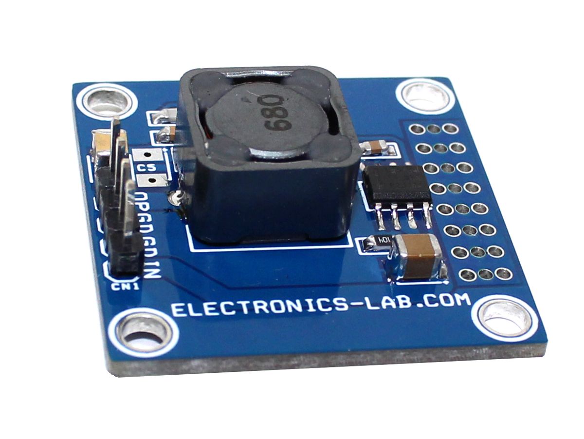
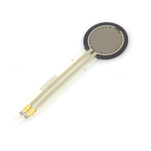
A common requirement for devices that must be sealed from environmental exposure is to replace all metal contact style push-buttons with functional replacements that do not have those weather-sealing difficulties. This article describes one such way of creating a contact button replacement using a Force-Sensitive Resistor (FSR) in conjunction with an SLG47004V.
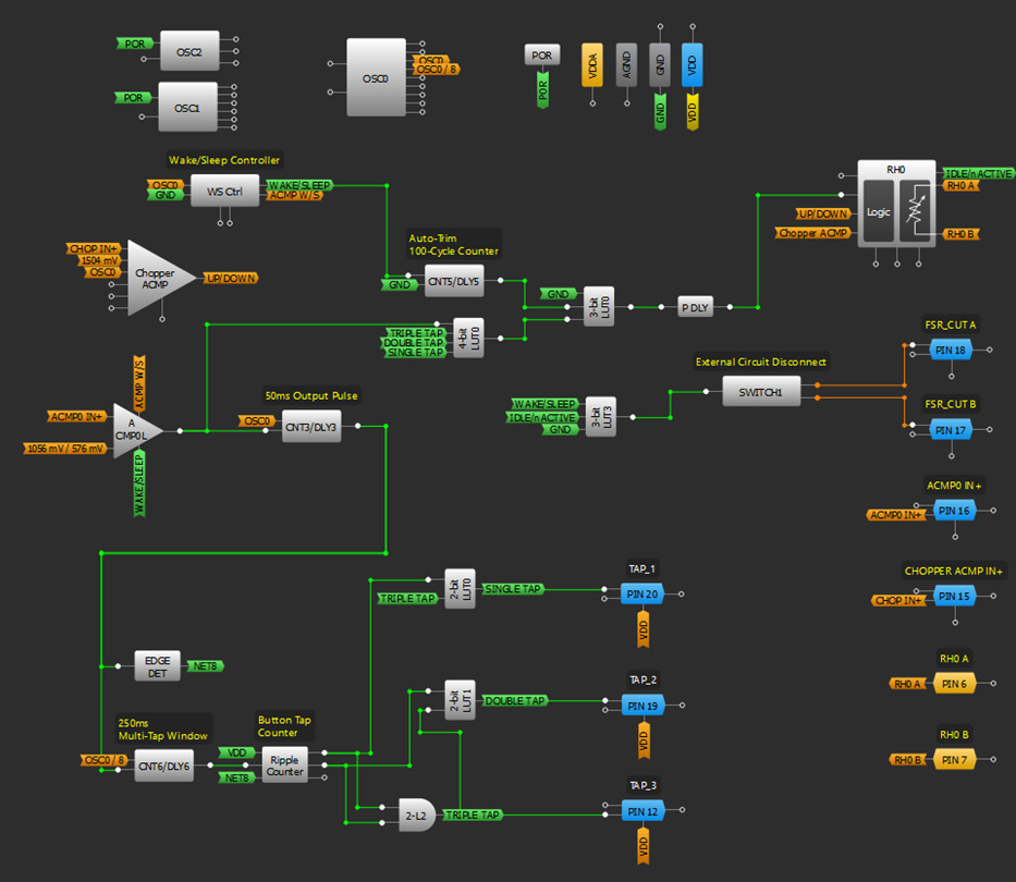
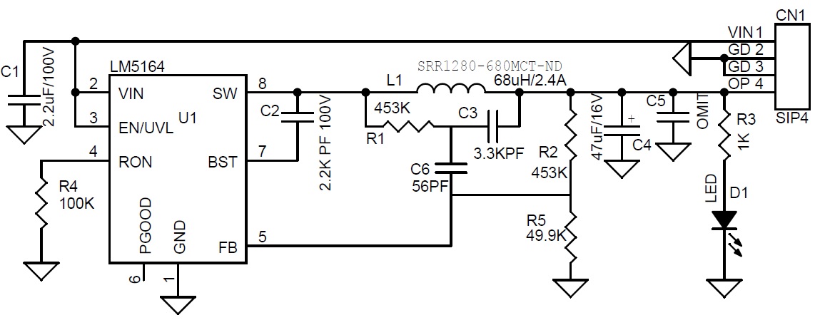
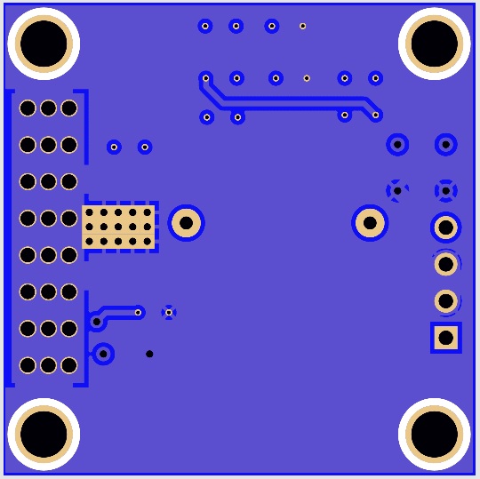
Schematic & Block Diagrams

Design Description
Overview
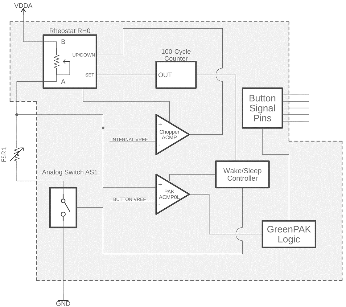
The design highlighted above is intended for use as a functional replacement for a metal contact style push-button while featuring ultra-low power consumption. Using an external force-sensitive resistor in series with one of the IC’s internal rheostat modules, a resistor divider network is created which is subsequently sampled by one of the SLG47004V’s internal low-power ACMPs. This ACMP determines the state of the button based on the voltage present at the divider output. Once the internal low-power ACMP determines that the button has been pressed, internal GreenPAK logic processes the button press signal to determine whether a single, double, or triple-tap has occurred, and outputs these signals to dedicated pins.
Since the force-sensitive resistor present in this design is highly susceptible to variation in resistance due to temperature changes, often as severe as +/-15% at extreme high/low temps, a constant “no-press” reference voltage must be maintained throughout a wide range of temperatures. This constant reference voltage is achieved using the circuit’s auto-trim functionality, which periodically samples the divider output voltage and adjusts the SLG47004V’s internal rheostat resistance, allowing the divider output to return to the specified “no-press” reference voltage. This auto-trim functionality not only allows for accurate operation over a wide range of temperatures, but it also allows the design to accommodate for sensor-to-sensor variations as well as variations in the overall system voltage level.
To attain ultra-low current consumption, the ACMP and external resistor divider network are controlled by the integrated circuit’s wake/sleep controller. This wake/sleep controller keeps the ACMP in sleep mode via matrix signal, and the resistor divider circuit in an open state via one of the IC’s internal analog switches, which is placed on the low side of the divider. The Chopper ACMP, which is responsible for the IC’s auto-trim functionality, is also indirectly controlled by the wake/sleep controller using an intermediate counter that triggers an auto-trim cycle once every 100 normal wake/sleep cycles.
Mechanical Pre-Loading of the FSR Sensor (Required)
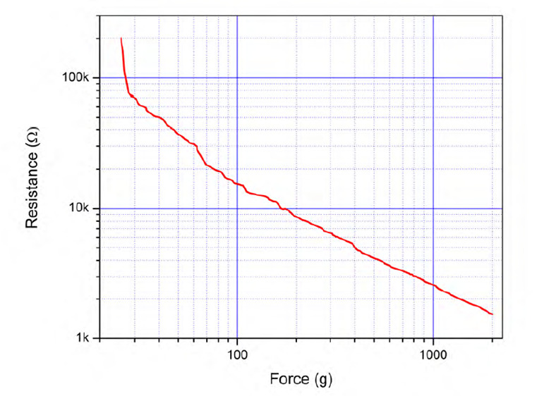
To properly trim the voltage divider circuit to the desired output voltage using the circuit’s digital rheostats, a small, consistent amount of force must be permanently applied to the FSR sensor before trimming can occur. This is due to the FSR’s very high no-load resistance, which measured over 100 MΩ in this test and is shown by the graph below, being far too large for the IC’s digital rheostats to compensate for. Pre-loading the FSR with a small mass will lower its base “un-pressed” resistance into a range that will allow the SLG47004V’s digital rheostats to properly trim the voltage divider. It is worth noting that this process does not require a specific force value to be applied, so long as the force applied satisfies two requirements:
- The applied force creates a large enough resistance drop within the FSR to allow for proper trimming of the voltage divider.
- The applied force remains constant throughout the lifespan of the application.
Auto-Trim Overview
To adequately implement an FSR sensor as a button replacement, considerations must be made for its rather large temperature dependency. Ideally, the no-press output voltage of the system would remain constant over temperature, allowing for a detecting ACMP to be tuned to detect button presses at all temperatures. Since the FSR’s resistance does not remain constant over temperature, the SLG47004V becomes responsible for maintaining this output voltage.
In this article, the circuit’s rheostats are used for their auto-trim capabilities, which adjust their resistance to match an internally generated reference voltage. This auto-trim process occurs whenever a high signal is provided to the rheostat’s “SET” pin. When this signal is brought high, either externally or via internal logic, the auto-trim process begins. A waveform of this process is provided at the end of this section, which shows the “SET” signal being brought high, and the voltage divider output voltage changing to match the internally set reference voltage which, in this waveform, is 1.5 V.
This auto-trim process, if implemented to occur periodically during the runtime of the device, will provide a very high level of consistency in the voltage divider’s output voltage. This, in turn, allows for one of the IC’s internal ACMPs to be used to detect press signals on the FSR and can be adjusted to detect presses at all temperatures within the range of the device.
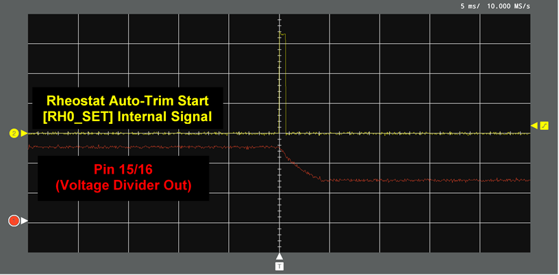
Vertical 1 V/div
Horizontal 5 ms/div
Results
Two points of functionality were measured to determine the success of the design. First, the design had to function as a button replacement, triggering the appropriate output signals in response to certain button-press sequences. Second, the device had to consume as little power as possible. Given that this type of design may be valued for its use in wearable technology, a maximum quiescent current of 10 uA was imposed as a design restriction.
Button-Press Functionality
Waveform captures of various operation conditions of the FSR button setup can be found below with accompanying descriptions and labels. VDDA was, in this test, set to 3.3 V and the FSR was given a small amount of mechanical pre-loading. Additionally, the auto-trim reference voltage was set to 1.5 V, and the rheostat’s “SET” signal was configured to be brought high by an internal counter block every 100 ACMP sample-cycles.
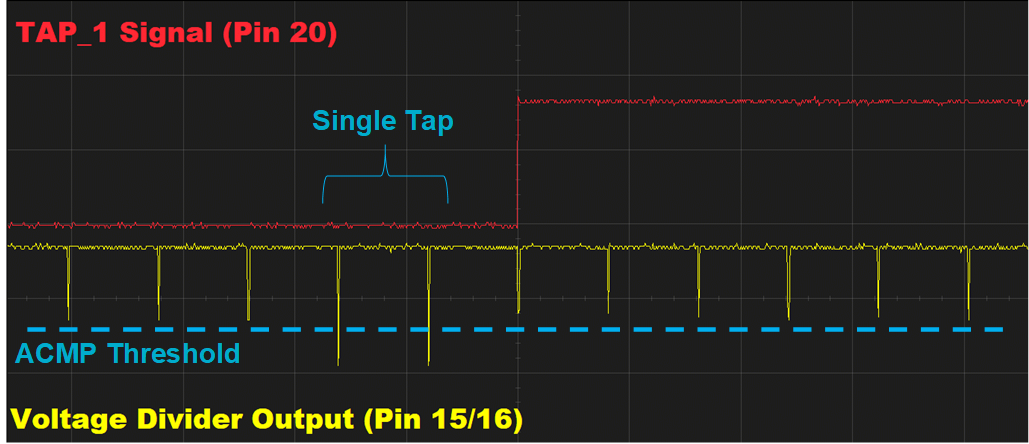
Vertical 1 V/div
Horizontal 50 ms/div
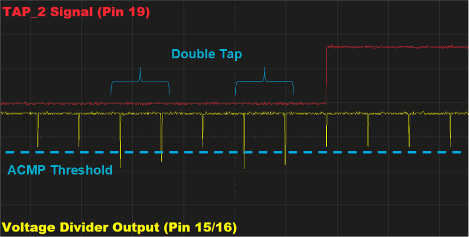
Vertical 1 V/div
Horizontal 50 ms/div
Current Consumption
Testing of quiescent current took place primarily at a sample rate of 25 Hz, as this is the lowest sample rate which seemed to provide an adequately responsive button design. A DC power monitor was used to capture the average Iq of the device, with external circuity included, over ten seconds, and the sample rate of said power monitor was set to 50 kHz for these tests. Below is the capture window of said DC power monitor:
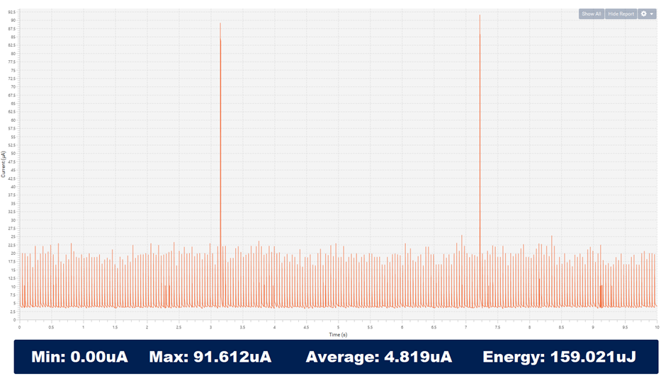
The two spikes present in the capture represent the auto-trim windows of the design, which are responsible for modifying the circuit’s internal rheostat value to allow the voltage divider in the above schematic to match a reference voltage. Since the device has already been properly auto-trimmed at this point, the SLG47004V’s internal chopper ACMP responsible for the auto-trim functionality is immediately turned off, thus resulting in a short spike. Each of the smaller spikes in the capture represents the circuit’s internal low-power ACMP being powered up to check if this reference voltage has dropped below a certain threshold, which would signal a button press has occurred.
The main testing parameter that prevents a higher level of precision when conducting this test is the fact that the force-sensitive resistor used in this design must be given a certain amount of mechanical “pre-loading” force for the resistance of the sensor to fall within a range that the circuit can effectively auto-trim. This sensor is very sensitive to not only the amount of force on the sensor but to the exact position of the force on said sensor. Since the sensor is too small for various reference weights to be used, the average active current measurements can be observed to fluctuate between 4 uA and 5 uA from test-to-test.
Conclusions
This design was tested at several sample rates, ranging from 10 Hz to 1 kHz. Of these sample rates, it was determined that to provide both adequate button performance and low power consumption, 25 Hz seemed to be the ideal ACMP sampling frequency. Under all tested conditions, however, the combination of SLG47004V and FSR proved to be a stable and well-performing button replacement solution.
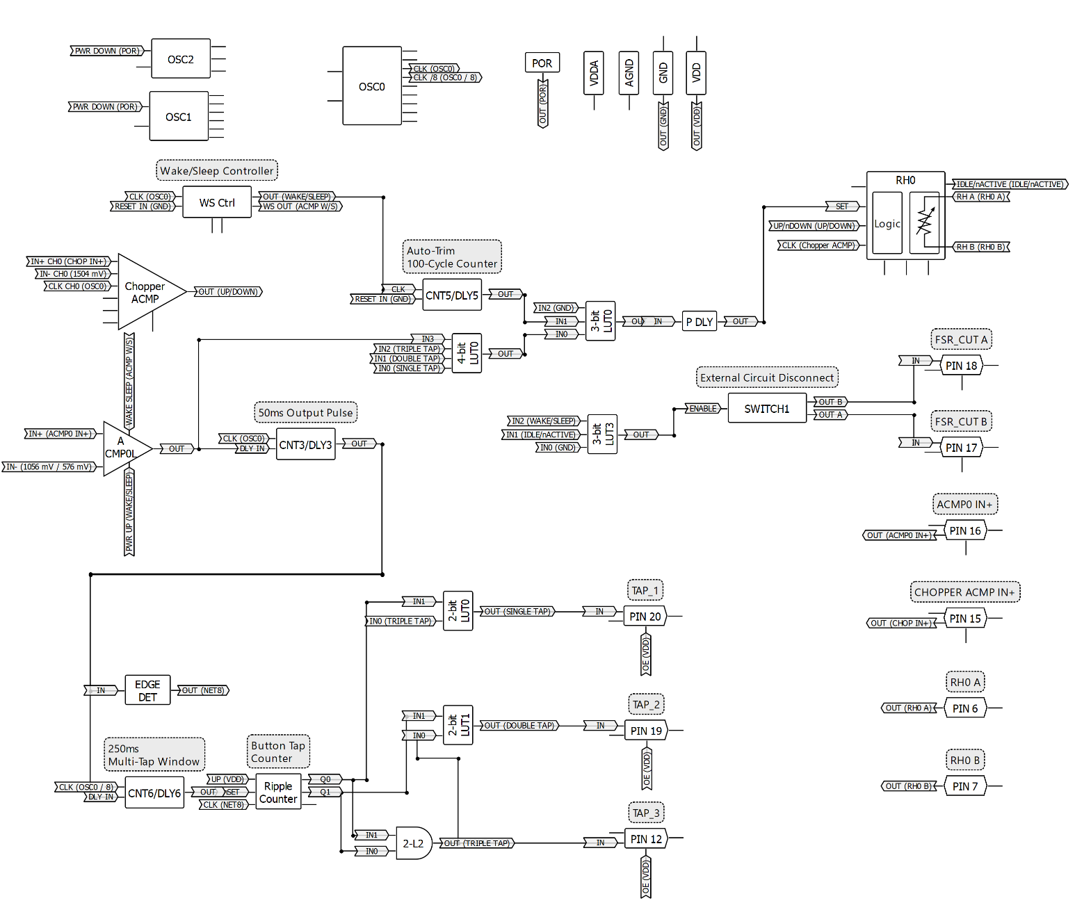
This IC design was created in free GreenPAK Designer software. The complete design file can be found here.
Appendix