Stefan Wagner published another project on github.com. He writes:
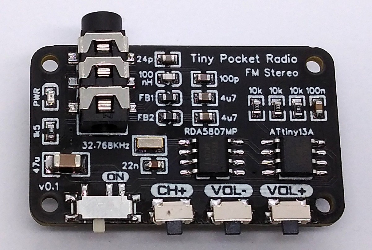
TinyPocketRadio is a simple FM stereo radio based on ATtiny13A and RDA5807MP. It’s powered by a CR2032 coin cell battery and can drive 32 Ohm headphones via the 3.5 mm audio plug. The board size is 38 x 23 mm. It has a power switch and three buttons: “Channel+”, Volume-” and “Volume+ “.
The low-cost RDA5807MP is a single-chip broadcast FM stereo radio tuner with fully integrated synthesizer, IF selectivity, RDS/RBDS and MPX decoder. The tuner uses the CMOS process, support multi-interface and require the least external component. All these make it very suitable for portable devices.
TinyPocketRadio – FM Stereo Radio based on ATtiny13A – [Link]
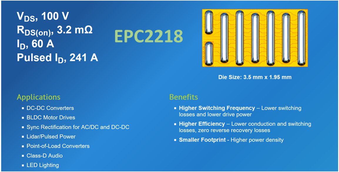
EPC’s 3.2 mΩ, 100 V, 231 Apulsed GaN transistor provides power efficiency and switching frequency
EPC’s EPC2218 transistors and development/evaluation boards supply 100 V, 60 A, and 231 APULSED enhancement-mode GaN FETs. The transistors are only supplied in passivated die form with solder bars and a die size of 3.5 mm x 1.95 mm. The EPC2218 is ideal for 48 VOUT synchronous rectification, Class-D audio, infotainment systems, DC/DC converters, and LiDAR for autonomous cars, robotics, and drones.
Features
Higher switching frequency for lower switching losses and lower drive power
Higher efficiency provides lower conduction and switching losses, as well as zero reverse recovery losses
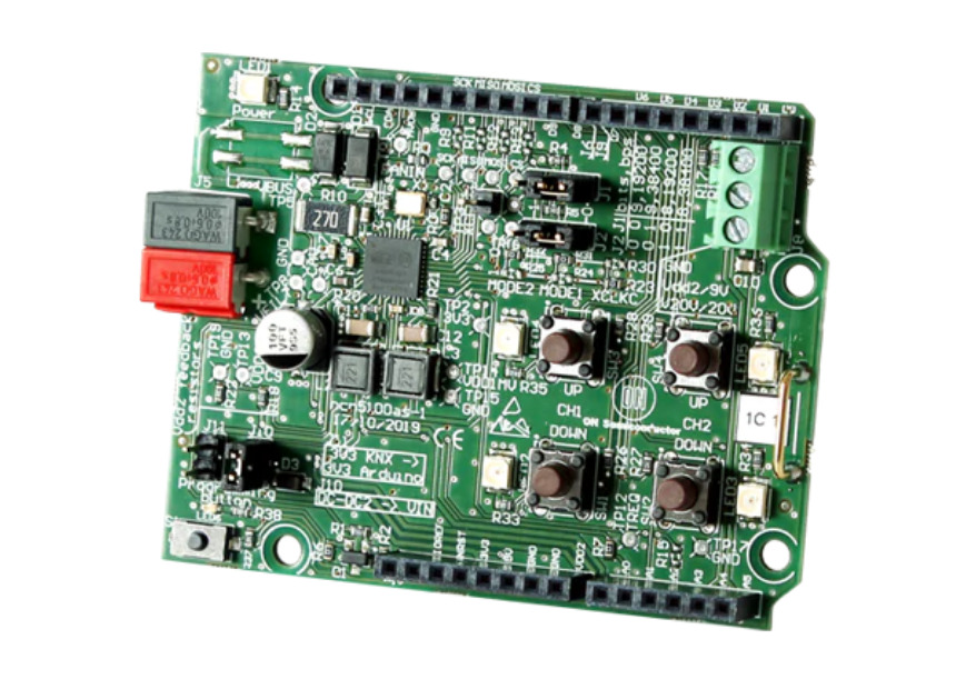
ON Semiconductor NCN51xxASGEVB evaluation boards are Arduino-compatible shields that enable rapid prototyping with a microcontroller of choice. These evaluation boards incorporate all the external components necessary for operating the transceivers. The NCN51xASGEVB boards come in three variants such as the NCN5110ASGEVB, NCN5121ASGEVB, and NCN5130ASGEVB. The NCN51xx series of KNX transceivers handle the low-level communication necessary to comply with the KNX standard. The NCN5110 is a bit transceiver and all the timings are handled by the microcontroller. The NCN5121 and NCN5130 implement the MAC layer that reduces the software development effort. The critical timings are handled by the transceiver.
Features
Arduino Uno V3 connectors ensure compatibility with a wide variety of development boards
Enable rapid prototyping
All external components necessary for operating the transceivers are included
Four onboard buttons/LEDs to build a dimmer application
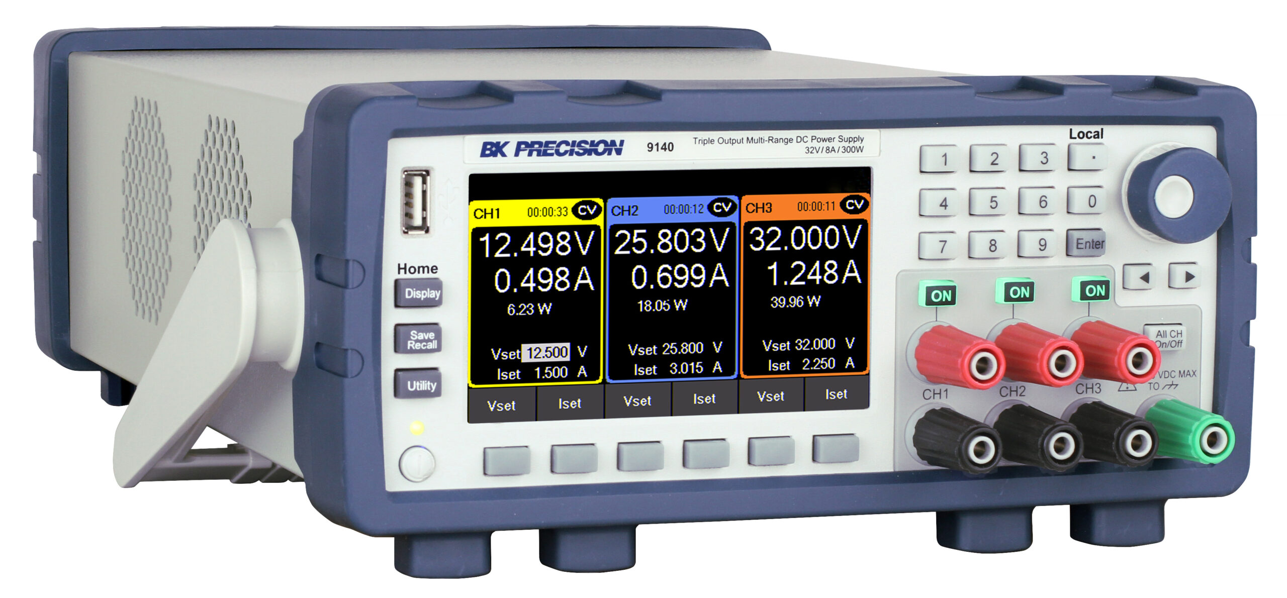
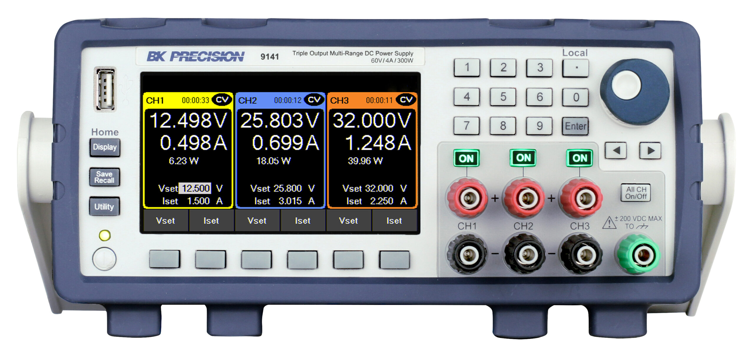
B&K Precision, a leading designer and manufacturer of reliable, cost-effective test and measurement instruments, today announces the 9140 Series Triple Output Multi-Range DC Power Supplies. With three isolated and individually controllable outputs, the 9140 (32 V, 8 A) and 9141 (60 V, 4 A) provide up to 300 W of clean power with low ripple and noise or 100 W per channel in a compact 2U half-rack form factor. The front panel features a 4.3-inch LCD and unique output terminals that support sheathed banana plugs or spade lug type connectors. Multiple outputs combined with advanced list mode programming, data logging, and extensive protection features make these power supplies suitable for a wide range of benchtop or test system applications.
This series offers several enhanced features not available on any of B&K Precision’s existing triple output power supplies. Powerful list mode features include list sequencing and step triggering for synchronizing events. List mode programs can be assigned to run on one or multiple channels simultaneously. Output sequencing allows users to link the output states between multiple channels with configurable on/off delays. Both models come equipped with LXI compliant LAN and USB (USBTMC-compliant and USBVCP) interfaces for remote control and programming with an optional GPIB interface. Remote control PC software, LabVIEWTM and IVI drivers are provided to simplify instrument control and test system integration. The USB host port on the front panel allows for logging voltage and current measurements directly to an external flash drive.
The 9140 Series is also cTUVus certified, indicating compliance with Canadian and U.S. National Safety Standards.
Available now, both models start at $1,850 and are backed by a 3-year standard warranty.
Features:
Three independent, floating output channels for up to 100 W per channel or 300 W total
High power density, compact 2U half-rack form factor
Multi-ranging operation
Low output ripple and noise down to 1 mVrms
Combine outputs to increase voltage up to 180 V or 24 A (depending on model)
Advanced and easy to use list mode programming
Channel coupling, tracking, configurable delays
Direct data logging to USB flash drive
Thermostatically-controlled fans for quiet operation
Adjustable voltage and current slew rates
OVP, OCP, OTP, and key-lock protections
USB (USBTMC-compliant) and LXI compliant LAN standard, GPIB option
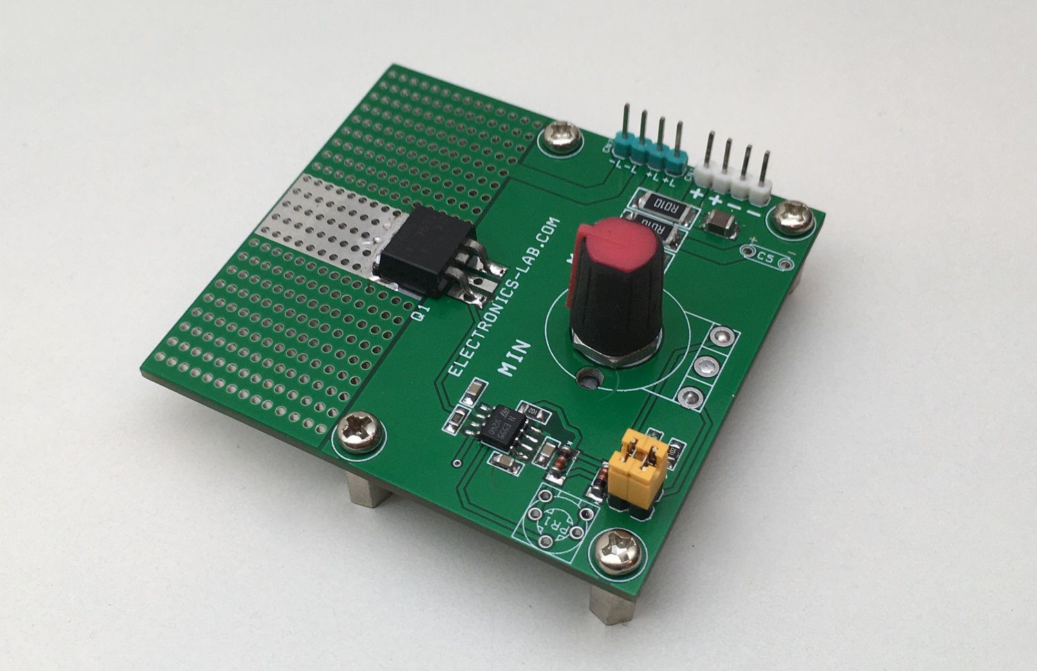
The project shown here is a cheap 60W LED dimmer for 12V LEDs/12V LED strips. The circuit is based on the very popular, versatile, and low-cost 555 timer IC, NE555 IC generates a PWM signal and IRF540 MOSFET works as output driver for the LEDs. In this circuit the 555 IC used in an astable multivibrator configuration to generate the PWM, by controlling the charging and discharging of the timing of capacitor C3, using D2, D3 and PR1. Potentiometer R7 is provided to control the intensity of LED connected to connector CN2, Connector CN1 provided to power the project with 12V DC. D1 is power indicator LED. Large thermal area provided as heatsink to cool down the MOSFET. The circuit can drive a load up to 36W (12V X 3Amps) in normal room temperature, and a load up to 5A requires forced air cooling for MOSFET Q1. D1 power LED, CN1 Power supply input, CN2 LED connections. R7 Potentiometer to control the intensity of LED.
60W LED Dimmer for 12V LEDs using 555 Timer – [Link]
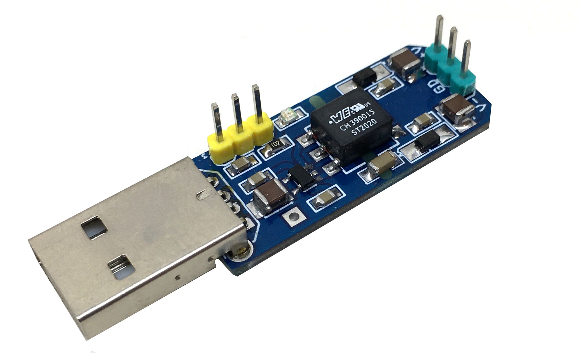
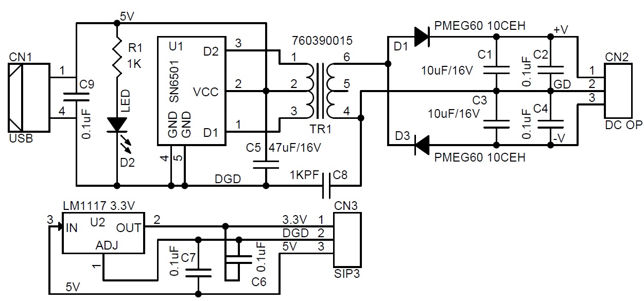
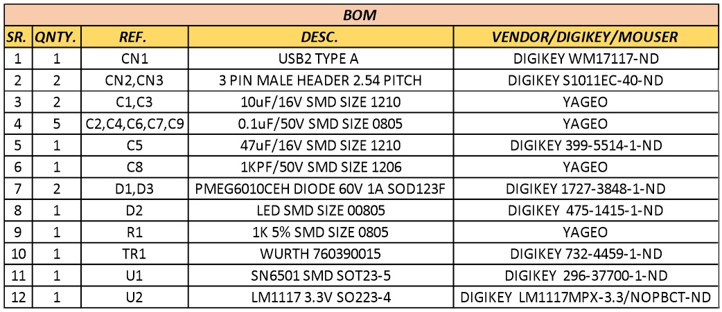
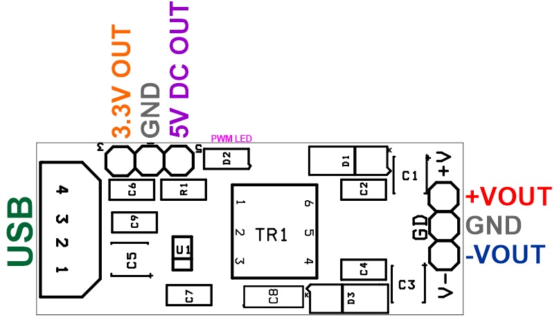
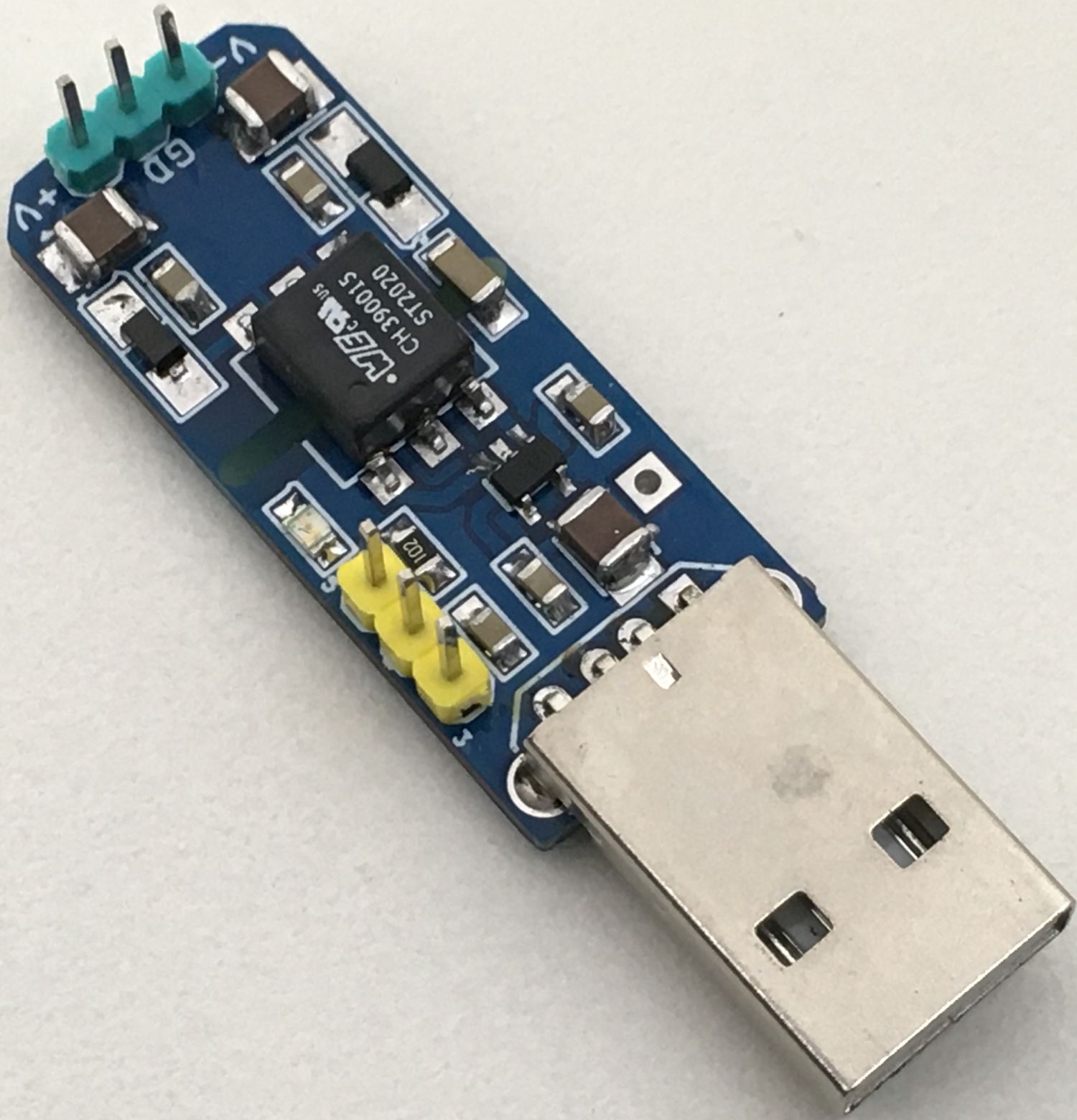
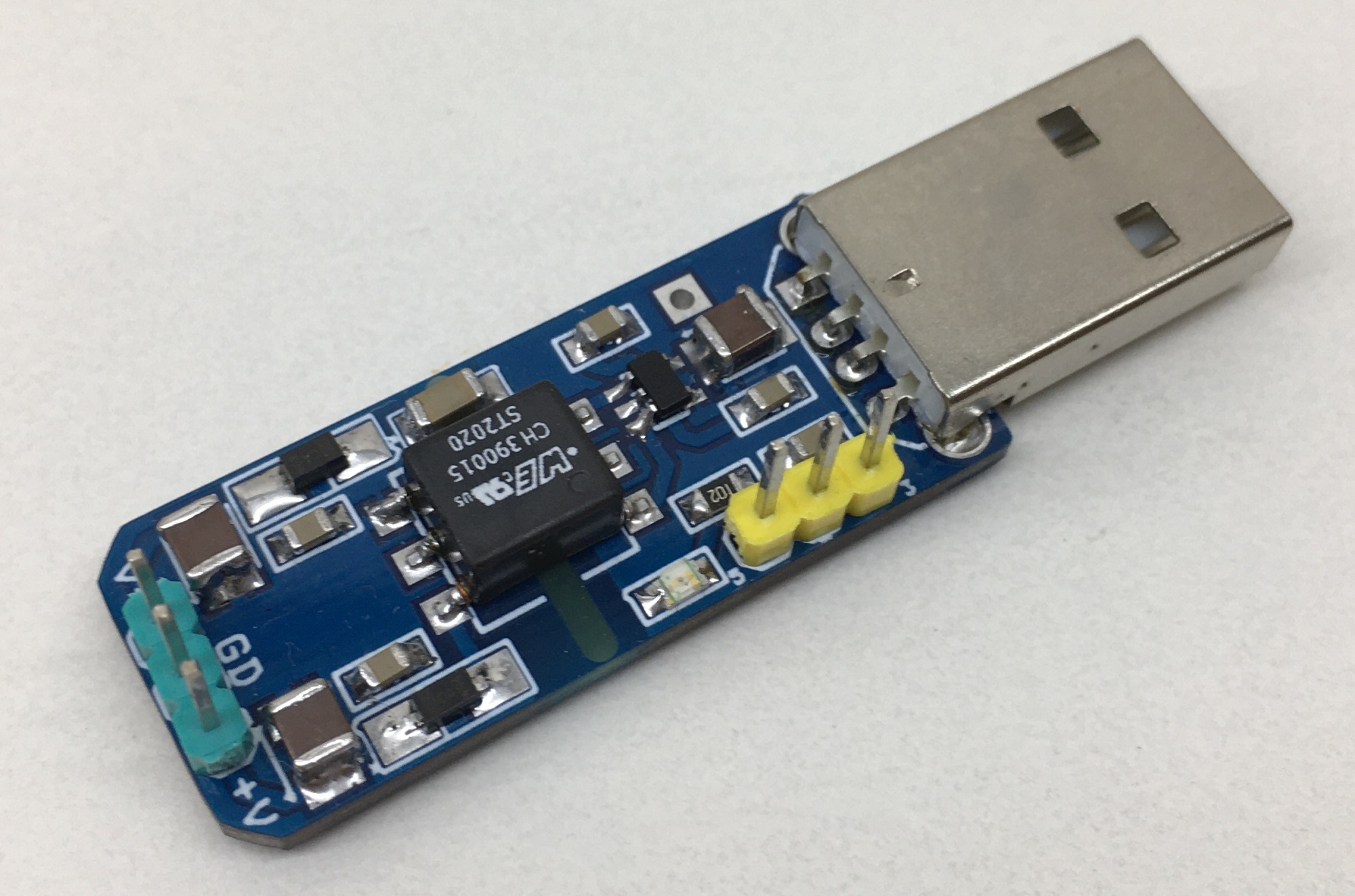
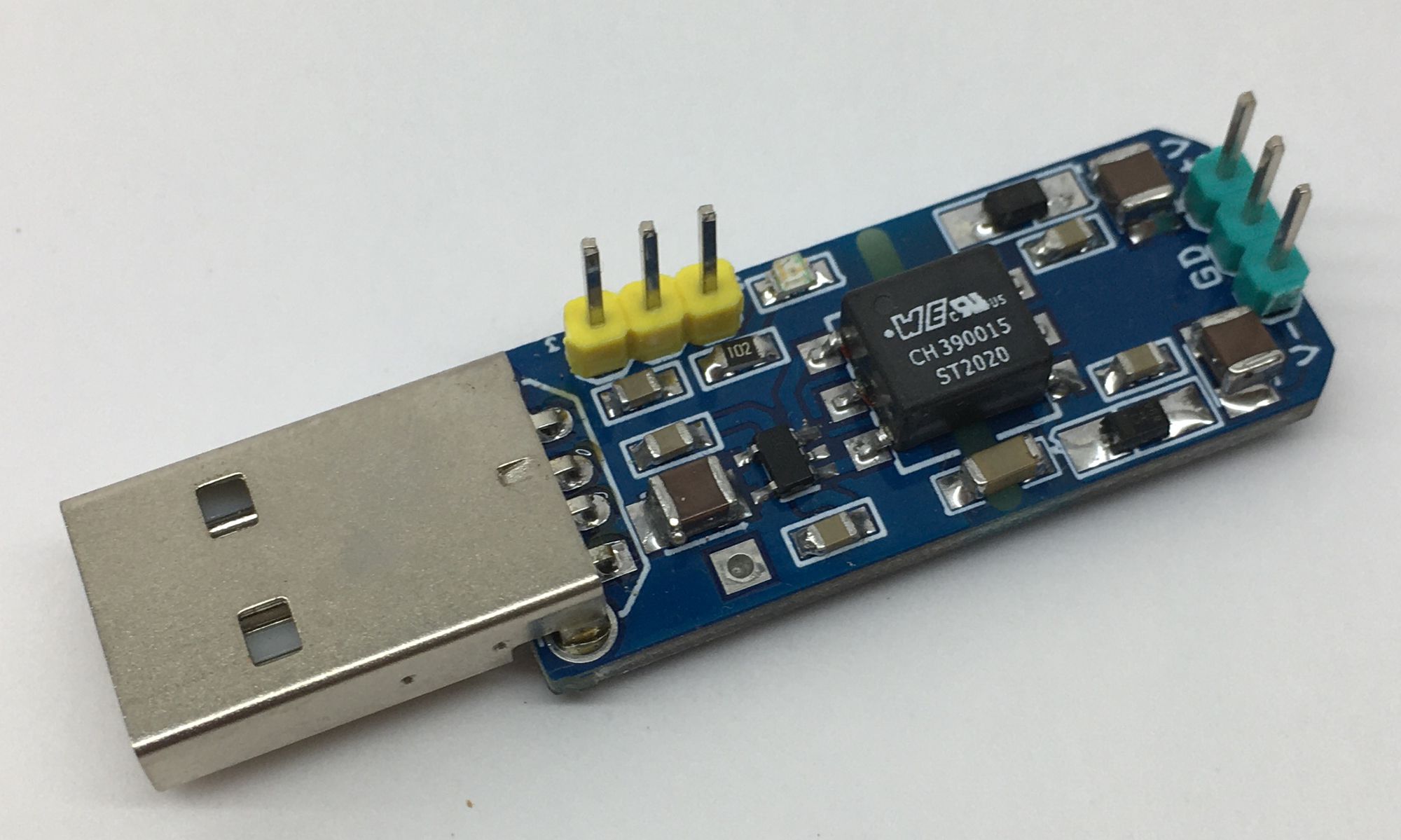
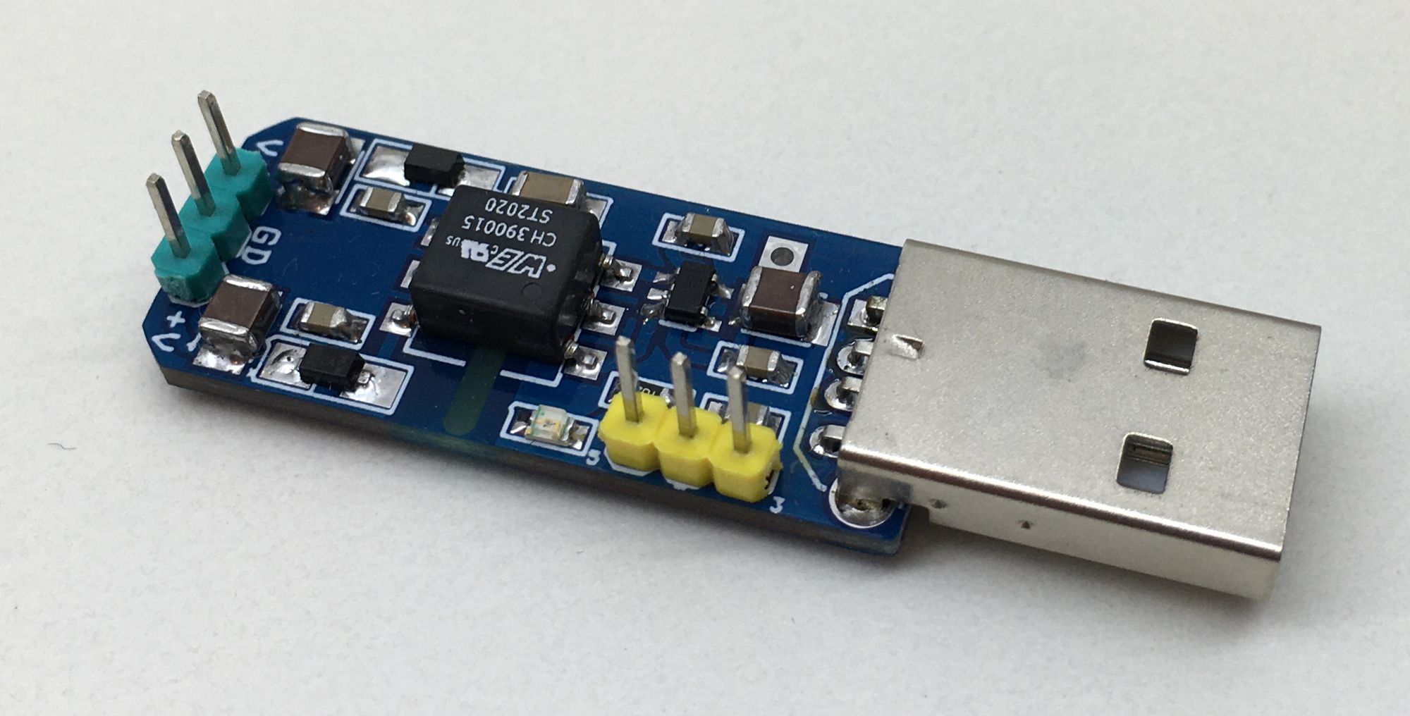
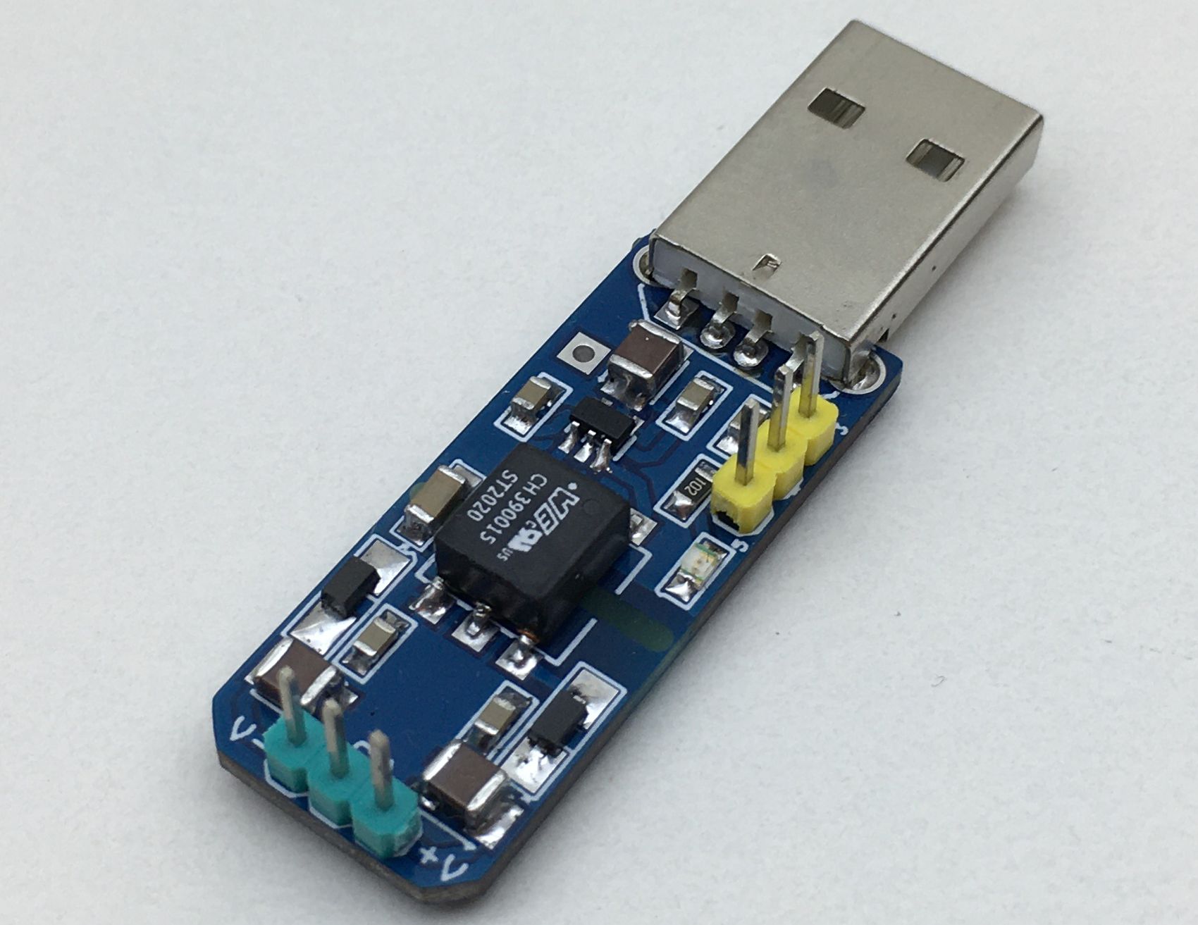
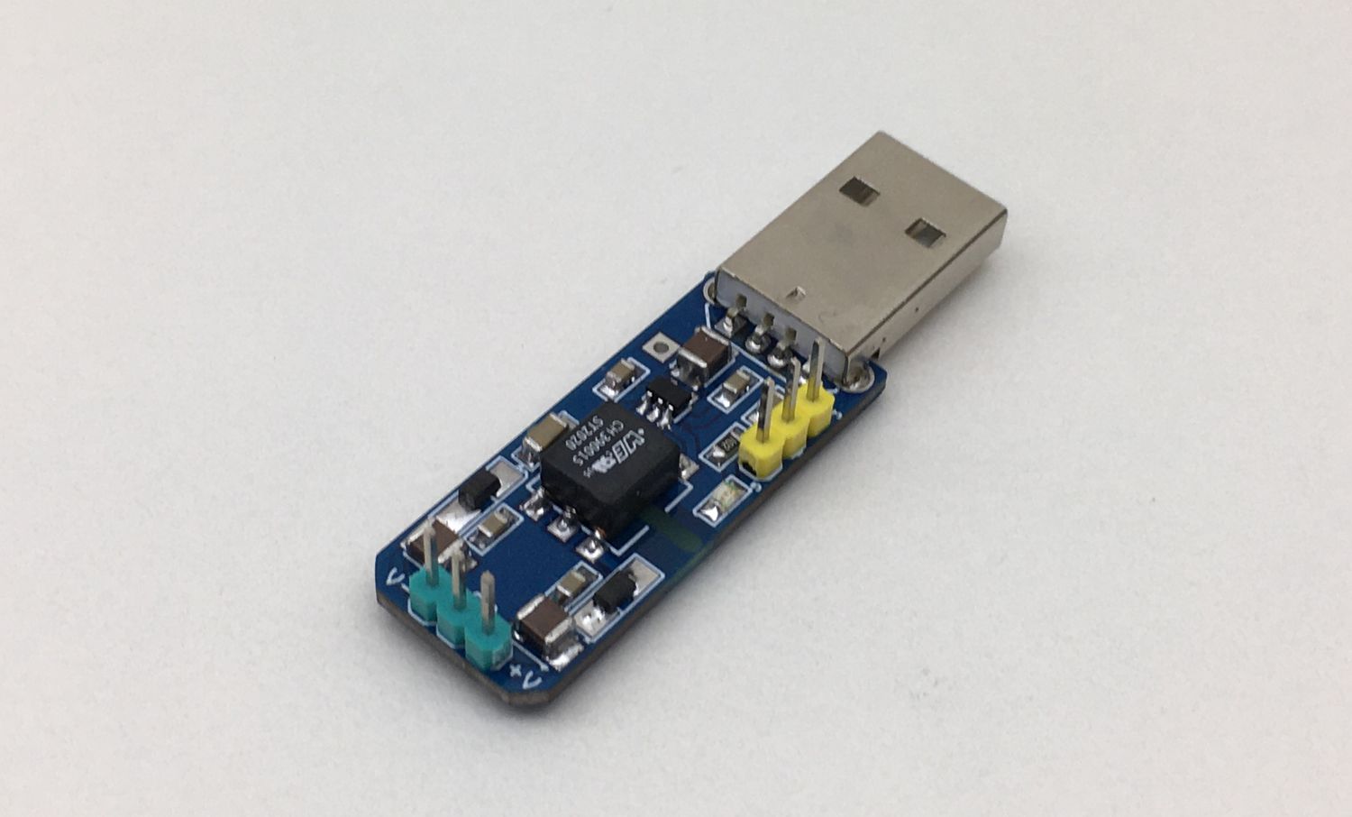
This is a mini DC-DC converter with dual output from single 5V DC supply or USB power source (e.g., +/-18V from 5V/USB). The mini board will fit into small space and perform with high efficiency. Basically, the circuit transfers power from 5V/USB to the output side +/-18V with high isolation, without a direct connection between 5V/USB power and output. The power isolation prevents ground loops and provides high noise immunity between input and output. The project is based on SN6501 chip, which is oscillator/power-driver, is specifically designed for small factor devices. The device drives a low profile, center-tapped transformer primary from 5V/USB power and secondary side provides unregulated dual output which can be further regulated as per requirement (e.g., +/-5V, +/-12V). Project is a very easy and simple tool to test and run industrial, scientific project, PLC and I/O modules which require dual output from single input. D2 power LED, CN1 USB A type connector for USB power input, CN3 No isolated 3.3V and 5V DC output, CN2 unregulated dual 18V Output.
SN6501 Oscillator: When the device supply has reached its nominal value ±10% the oscillator is fully operating. However, variations over supply voltage and operating temperature can vary the switching frequencies between 300 kHz and 620 kHz for VCC = 5 V ±10%
The SN6501 is a transformer driver designed for low-cost, small form-factor, isolated DC-DC converters utilizing the push-pull topology. The device includes an oscillator that feeds a gate-drive circuit. The gate-drive, comprising a frequency divider and a break-before-make (BBM) logic, provides two complementary output signals which alternately turn the two output transistors on and off. The output frequency of the oscillator is divided down by an asynchronous divider that provides two complementary output signals with a 50% duty cycle. A subsequent break-before-make logic inserts a dead-time between the high-pulses of the two signals. The resulting output signals, present the gate-drive signals for the output transistors. As shown in the functional block diagram, before either one of the gates can assume logic high, there must be a short time period during which both signals are low and both transistors are high impedance. This short period, known as break-before-make time, is required to avoid shorting out both ends of the primary.
Note: Other than isolated +/-18V, the circuit also provides 3.3V DC @ 150mA and 5V DC @ 200mA. Both 3.3V and 5V outs are non-isolated.
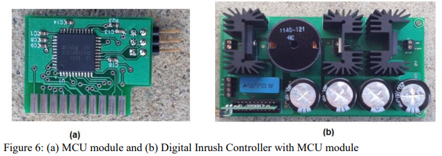
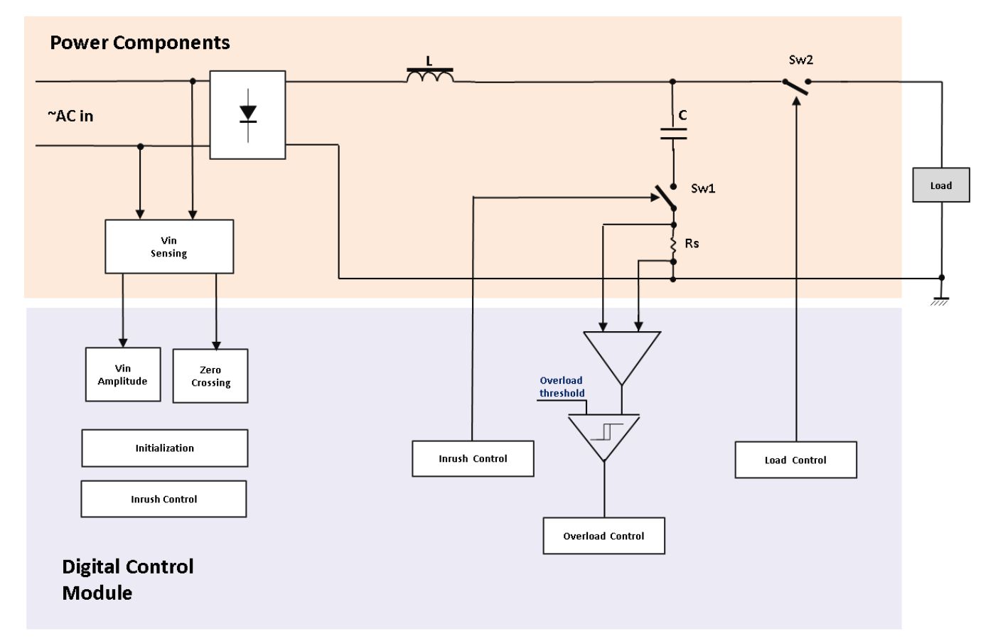
App note from IXYS about their unique digital inrush controller using Zilog’s 8-bit Z8F3281 MCU.
Digital control allows distinctive solutions to control inrush current in typical AC-DC rectifier with capacitive load by limiting capacitor pre-charge current to a predetermined value at each half sine-wave cycle. Capacitor charge is spread over a number of cycles until capacitor is charged proportion of peak value of AC voltage source. Capacitor is charged according to timedependent pulse train. The pulses are designed in a way to provide substantially equal voltage increment applied to capacitor to keep peak of charging current about the same value at each cycle. Number of cycles depends on capacitor value and charge current. For a given capacitor value which is selected depending on desired ripples amplitude, the charge current is a function of number of pulses and its timing position with respect to rectified sine wave. Detailed algorithm of creating pulse train for Digital Inrush Control is described in the Principles of Operation section.
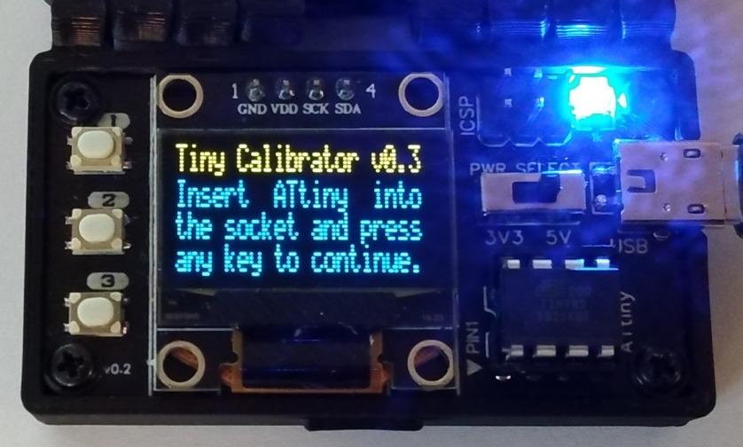
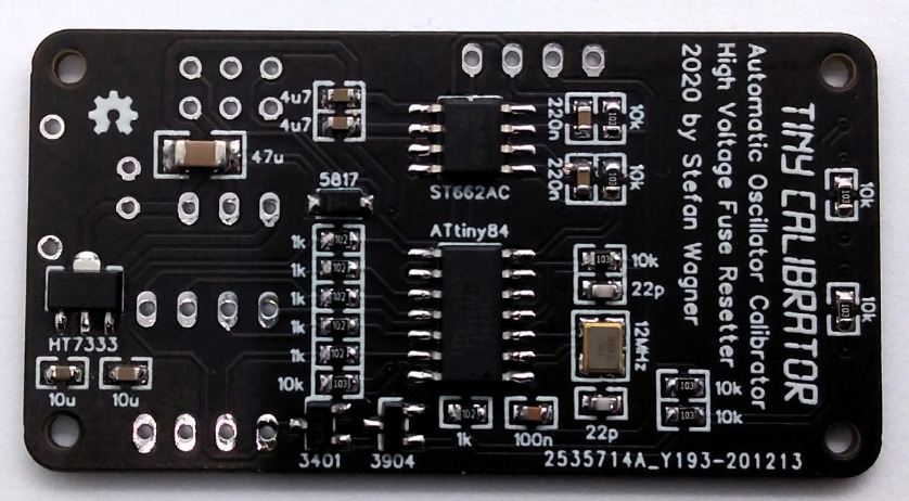
A GitHub user called Wagiminator has posted details about ATtiny84-TinyCalibrator, which is an OSC Calibrator and High Voltage Fuse Resetter for 8-Pin ATtinys. The ATtiny84 was chosen as the microcontroller for the TinyCalibrator because it has exactly the necessary number of GPIO pins. 8-pin ATtinys usually feature few GPIO pins available, so they are usually operated without an external clock. However, its internal oscillator performs well in most applications, but when it comes to precise timing, its +/-10% accuracy is often insufficient. This problem can be solved, the oscillator can be calibrated, therefore increasing its accuracy to +/-2% or more. You can perform this calibration in various ways, and the TinyCalibrator can do this fully automatically by a push of a button.
For the project hardware, Wagiminator made use of a micro USB connector to supply the TinyCalibrator with 5V. He also integrated an HT7333 voltage regulator to power the oscillator. Then he added a switch which he used to to choose whether the oscillator should be powered for 3.3V or 5V. To give out accurate frequency measurements, he operated the ATtiny84 with an external 12 MHz crystal. Since the current software version only requires about 3.7 kByte, an ATtiny44 can also be used. He chose an ST6624 charge pump IC to generate the 12V for the High Voltage Serial Programmer, which was specially designed for such applications and needs only a few external components. The 12V was controlled by a MOSFET and applied to the RESET pin of the target ATtiny if need be, then he protected the remaining programming lines to the target against a short circuit with resistors. For the user interface, He utilizes three buttons and a 128×64 pixels OLED display.
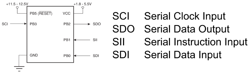
In order for him to carry out the calibration, he uploaded a program to the target ATtiny using the integrated High Voltage Serial Programmer. Also, the factory oscillator calibration value (OSCCAL) is written to the EEPROM. The software programming on the target ATtiny reads the EEPROM and writes the value to the OSCCAL register. It then applies an oscillating signal with half the clock frequency to pin PB0. He notes that “Since the fuses were previously set so that the target ATtiny runs with a prescaler of 8, a signal with 1/16 of the oscillator frequency is applied to PB0.” The code for the High Voltage Serial Programmer (HVSP) has a spectacular approach. The way it is designed is that for each action, a series of instructions are sent over the data lines to the target ATtiny and the corresponding response is read. The process and the instructions are well described in the data sheet above. For the frequency measurement, the timer/counters of the ATtiny84 carry out the measurement. The oscillator frequency of the target ATtiny can be calculated easily. He connected the PB0 of the target ATtiny, which outputs a signal with 1/16 of its oscillator frequency to the T0 input of the ATtiny84, the Timer0 then counts the pulses at T0 and timer1 stops the measurement after a time of 32 milliseconds.
To operate the device, you carry out the following processes:
You select the desired supply voltage (3.3V or 5V) with the switch.
You connect a 5V power supply to the micro USB port.
Then place the ATtiny13/25/45/85 in the IC socket and press any key. Note: use an SOP adapter for SMD parts.
Finally, select the function you want and follow the instructions on the display.
You can find more information about the project, and how it functions on his GitHub page.
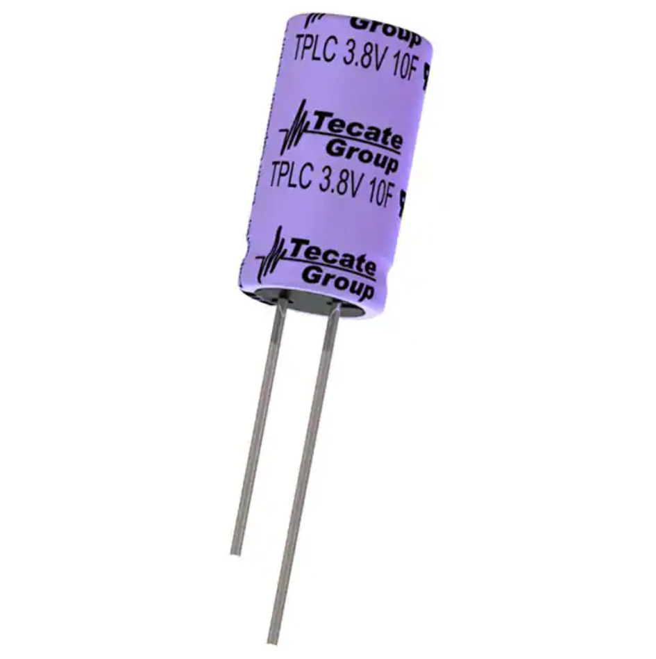
Τecate Group’s TPLC series combines the high power density of an ultracapacitor and the rich energy density of a lithium battery
Tecate Group’s TPLC series is UL recognized and RoHS and REACH compliant. The capacitors are ideally suited for applications requiring increased voltage, higher energy density, and an exceptional cycle life that is not available with standard EDLC technology or lithium-ion batteries alone. For industrial applications where essential machine controllers can be impacted by unplanned interruptions, ride through power is provided to mitigate these effects. The TPLC series provides critical pulse power that is required in gas/water utility meters where long cycle life and low self-discharge are essential for efficient and reliable operation. These capacitors are well-suited for data centers where reliable, economical, and compact energy solutions that address the potential loss of cache memory, RAID systems, and storage servers that can be impacted by unplanned power outages are necessary.
Features
Combines the long life (calendar and cycle) characteristics of the ultracapacitor with the high energy density of the Li-ion battery
Volumetric efficiency in small can size with low resistance: 10°F to 450° F
Broad operating temperature range: -25°C to +70°C
Safety: low self discharge, no thermal runaway, open failure with use of safety vent
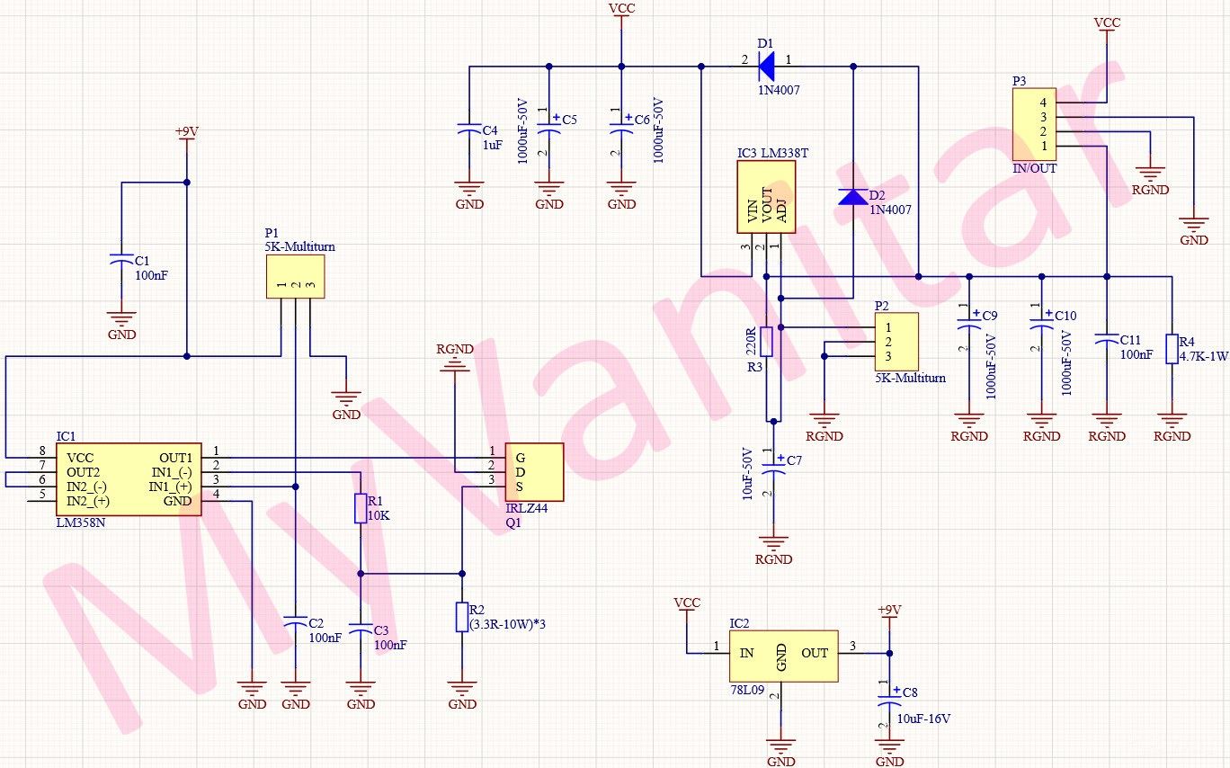
In this article/video, I introduced an adjustable 30V-4A linear power supply that provides constant voltage and constant current adjustment. The output noise of the power supply is low and has measured using the power analysis feature of the Siglent SDS2102X Plus oscilloscope. All component packages are through-hole, so you don’t need any special tool for soldering. Let’s get started!
Specifications
Input Voltage (max): 35V [30V, max-tested]
Output Voltage (min): 1.28V
Output Voltage (max-tested): 27.35V [28.9Vin, no load, 25C]