Glasgow Interface Explorer is a Hardware Debugging Tool for Digital Electronics

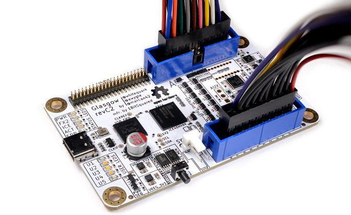
1BitSquared has launched a crowdfunding campaign for a highly capable and extremely flexible open source multi-tool called Glasgow Interface Explorer.

Glasgow Interface Explorer for digital electronics is powered by Lattice Semi iCE40 FPGA and created for hardware developers, electronics hobbyists, engineers, tinkerers, and

“anyone else who wants to communicate with a wide selection of digital devices with minimum hassle.”

The board aims to offer a broad selection of capabilities with more than “some wires and, depending on the device under test, external power.” You can attach it to devices without any need for extra active or passive components.

Some of its Key Features and Specifications include: 

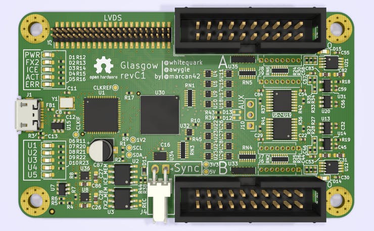
  • iCE40HX8K Lattice Semiconductor FPGA
  • 1x USB-C port connected to FX2 high-speed USB interface; 480 Mbps throughput
  • 2x 8-channel GPIO banks, each with:
    • A dedicated programmable linear voltage regulator, configurable from 1.8 – 5V with up to 150 mA of power
    • A dedicated sense ADC capable of monitoring the GPIO bank voltage and current, with interrupt trigger thresholds that can be set
  • 16 highly flexible GPIOs, each with:
    • A peak frequency of 100MHz
    • A dedicated level shifter with individual direction control, and,
    • An independent, software-controlled 10K Ohm resistor Pull-Up/-Down resistor
  • ESD protection diodes for all GPIOs
  • Set of 14x differential pair I/O, connected directly to the FPGA (optional); can be used for high speed interfaces
  • Up to 5x User-controlled LEDs
  • Up to 5x Status LEDs, and,
  • 1x Dedicated SYNC connector

The software is fully in Python 3, including the FPGA logic, which is described with a Python-based domain-specific language.

“The Glasgow software is a set of building blocks designed to eliminate incidental complexity. Each interface is packaged into a self-contained applet that can be used directly from the command line or integrated into a more complex system. Using Glasgow does not require any programming knowledge, though it is much more powerful if you know a bit of Python.”

says 1BitSquared.

Glasgow is highly flexible since it is based on an FPGA, and can do a number of things like: 

  • Communicate via UART with automatic detection of the baud rate required
  • Initiate SPI and I2C transactions
  • Read and write to and from 24-series electrically erasable programmable read-only memories (EEPROMs)
  • Read and write 25-series flash memories
  • Read and write any ONFI-compatible flash
  • Program and verify AVR microcontrollers over SPI
  • Play back JTAG SVF files
  • Debug ARC processors over JTAG
  • Debug a subset of MIPS processors via EJATG
  • Program and verify XC9500XL CPLDs
  • Determine unknown JTAG pinouts automatically
  • Read raw modulated data from 3.5″  and 5.25″ floppy drives

The board is currently available through a crowdfunding campaign that was launched recently on Crowd Supply with a USD 25,000 funding goal. The campaign has so far raised more than USD 154,000 with over 850 backers and it will still be on for the next one month. You can get the latest RevC revision of the board with a full set of flywire, sync, and USB-C cables for $139 and another package with an optional CNC-milled and anodized aluminum case for $189.

The project is also entirely open source, and all hardware design files, firmware, software and documentation are available on Github.

Further details can also be found on the project’s page on crowd supply.

Headphone Amplifier For DAC Converter

This is a headphone amplifier project for audio digital-to-analog converters (DACs) with differential voltage outputs. This circuit converts the differential voltage output of the DAC to a single-ended, ground-referenced signal and provides the additional current necessary for low-impedance headphones. Project is built using OPA1688 low distortion, high-drive Sound Plus audio amplifier. The circuit tested with dual +/-5V DC supply, and it can drive a load 16 Ohms to 600 Ohms. Headphone amplifier provides an output 50mW into 32 Ohms. Signal for the right channel and left channel input is applied to the amplifier through connectors CN1and CN3, respectively.

Headphone Amplifier For DAC Converter – [Link]

Maxim Integrated MAX17623/MAX17624 Evaluation Kits

Maxim Integrated MAX17623/MAX17624 Evaluation Kits is configured to evaluate the MAX17623/MAX17624 Step-Down Converters’ operation. The MAX17623/MAX17624 Step-Down Converters are part of the Himalaya series of products that enable cooler, smaller, and simpler power supply solutions. The devices are configured to demonstrate optimum performance and component sizes in the Evaluation Kits.

The Maxim MAX17623/MAX17624 Evaluation Kits feature provisions for selecting the mode of operation (PWM/PFM), enabling or disabling the output and PGOOD signal.

Features

  • 2.9V to 5.5V Input-voltage range
  • MAX17623 Offers high 92.2% efficiency (VIN = 3.3V, VOUT = 1.5V, IOUT = 300 mA)
  • MAX17624 Offers high 94.5% efficiency (VIN = 5V, VOUT = 3.3V, IOUT = 500 mA)
  • Selectable PWM and PFM modes of operation
  • Internal 1ms soft-start time
  • PGOOD Output with pullup resistor to respective input voltages
  • Low-profile, surface-mount components
  • Proven PCB layout
  • Fully assembled and tested

more information: https://datasheets.maximintegrated.com/en/ds/MAX17623EVKIT-MAX17624EVKIT.pdf

Texas Instruments TLV767 Positive Voltage Linear Regulators

Texas Instruments TLV767 Precision Positive Voltage Linear Regulators are a wide input linear voltage regulator that supports an input voltage range from 2.5V to 16V and up to 1A of load current. The output range is from 0.8V to 6.6V or up to 13.6V in the adjustable version. Additionally, the TLV767 has a 1% output accuracy that can meet the needs of low voltage microcontrollers (MCUs) and processors.

The TLV767 is designed to have a much lower IQ than traditional wide-VIN regulators, thus making the device well positioned to meet the needs of increasingly stringent standby power requirements. When disabled, the TLV767 draws only 1.5µA of IQ. The internal soft-start time and fold-back current limit reduce inrush current during startup, thus minimizing input capacitance.

Features

  • VIN: 2.5V to 16V
  • VOUT
    • 0.8V to 13.6V (Adjustable)
    • 0.8V to 6.6V (Fixed, 50mV Steps)
  • 1% Output Accuracy Over Load and Temperature
  • Low IQ: 50µA (Typical, ~1.5µA in Shutdown)
  • Internal Soft-Start Time: 500µs (Typical)
  • Fold-Back Current Limiting and Thermal Protection
  • Stable With 1µF Ceramic Capacitors
  • High PSRR: 70dB at 1kHz, 46dB at 1MHz
  • Temperature Range: –40°C to +125°C
  • Package: 6-Pin 2mm×2mm WSON

Wide bandwidth PSRR performance is greater than 70dB at 1kHz and 46dB at 1MHz, which helps attenuate the switching frequency of an upstream DC/DC converter and minimizes post regulator filtering. To allow for more flexibility, the TLV767 has both fixed and adjustable versions.

more information: https://www.ti.com/product/TLV767

RGBDuino UNO and RGBDuino RGB Shield: Add Light and Questionable Arduino PCB

Now, from my writing experience here at eLab, I have dealt with some funny and interesting concepts, but nothing quite like what I am about to show you. But bear with me here, aside from the questionably looking electronics you are about to glance, there might be something useful to light up your Arduino projects. So, take this article with a grain of salt, as things will get very weird, very fast.

So, what is there so special about the RGBDuino? Firstly, we are talking about an RGB shield for Arduino, constituted by 40, individually addressable, RGB LEDs. It allows for a flexible 5 and 3.3 V inpt logic, as well as operate under the 3.5 to 5.3 V range, so nothing very limiting there. Speaking of limitations, you only need one pin to control it, and you also have a 24-bit color resolution, which is really good. It can be powered via the Arduino directly (with a mere 2 A of maximum operating current, are you sure you want to do that?), or via an external source. Regarding safety, it incorporates a reverse polarity protection diode for the external power port. Being compatible with the Arduino interface, it makes an ideal candidate for your projects where lightling is important. The last two things to take into consideration are a digital output connection, for you to expand the 40 LEDs to more, if you desire, and the adition of a reset button, so that you do not injure yourself trying to reach for the button on the bottom of the board, if necessary.

The RGBDuino shield
The RGBDuino shield

Now, everything discussed so far does not seem ridicule, in any way, so let us embrace the weirdness that accompanies this product. You can only get the RGBDuino shield if you get a very questionably looking Arduino UNO compatible board, the RGBDuino UNO. Do not get me wrong, it is a fully-fledge and dignified version of an Arduino, but they went with a very unusual looking PCB, which comes in the form of an anime woman (and I describe: half-naked, holding a soldering iron, the right way at least) named Jenny, or an intelectual-looking duck with glasses and dungarees. Why am I complaining? They look amazing! Well, they did not name the duck, and that bothers me.

Is this the part where I get fired?

After what we have seen so far, you may be wondering: what’s the use of an image on top of a PCB if I am going to hide it with a shield? Well, do not hide it. It is worth much more, use an Arduino for the shield instead, and get a transparent case to the Arduino board! Lastly, as I said, you can only get this in bundle with Jenny or “duck”, and it will be $18.67, which is not bad, considering the creativity put into it (and the fact that LED shields are quite expensive).

When I said to not hide the board, here is a suggestion

Watchy: The Open-Source E-Paper Watch

The good thing about Tindie is that allows all of us to creatively showcase and sell our most promising projects. I cannot stress how awesome it is to have such a market online, for our inventions! As a good example of its usefulness, we will glance today at an e-paper watch that has the potential to do so much, the Watchy!

Created by SQFMI and hosted on Tindie, the Watchy is an open-source (hardware and software) e-paper watch, that consists of a single PCB, with the connectors for a battery and an 200 x 200, e-paper display. While its display gives you a unique vibe, not really usual in a watch, the wearable is also a very promissory development platform, due to its hardware and the easiness to program it to incorporate different functionalities: it can be stated as an innocent watch, but can go far beyond that scope. Besides that, its appearance can be customized with no fuss, through 3D printed cases and different watch straps.

Watchy, dissected
Watchy, dissected

By taking a deeper dive into its internals, you can see why we have done nothing but compliment this innofensive timepiece. At the heart of the PCB there is an ESP32, giving you the Wi-Fi and Bluetooth capabilities most smartwatches rely upon these days. When it comes to sensors and actuators, you are well served: a motor, some tactile buttons, an accelerometer… and more obviously, the serial-USB adapter for programming / charging and an RTC (because at the end of the day, it is still intended to be a watch).

Taking a look at the specs, here is what you will find:

  • Ultra-low-power, 1.54″ e-paper display, with a resolution of 200 x 200 and wide viewing angles
  • ESP32-PICO-D4 MCU, with Wi-Fi and Bluetooth connectivity
  • 3-axis accelerometer with gesture detection capability
  • Vibration motor
  • 4x tactile buttons, located on the sides
  • Open-source hardware and software architecture; many watch faces + examples available on GitHub and 3D case designs + watch straps
Watchy and its inner beauty

As you can see here, the Watchy has the potential both as a product and also as a handheld development platform, for you to unleash your creativity upon. It even has a website entirely dedicated to it! We do not see many alternatives on the market, beside some Arduino-based projects, but this one here is something else, in my humble opinion. One thing I do not know for sure is the e-paper display, I do like a bit of color, so I would like to see them release an alternative display, just because I think it would bring even more attention to it. Lastly, let us discuss price: for $44.99 (in sale right now) you can get the complete Watchy. If you are int he market for something similar, it is a no-brainer!

Even the case is cooler than the cool kids

Meet Qomu – A complete SoC that easily fits inside a USB port

Tomu family of USB devices has recently introduced a small form factor board that is not only a single MCU or an FPGA, but a complete System-on-chip that fits easily inside a USB port.

The tiny compact board called Qomu, is a capable USB device that integrates an EOS S3 low-power MCU and an eFPGA with 100% open source tools. The MCU can run up to 80 MHz while the embedded FPGA has about 2,400 effective logic cells and up to 64 Kbits of available embedded RAM.

Whether it’s a glue logic for a new peripheral or an accelerated machine learning classifier that you need, the EOS S3 SoC makes it easier to make fine-grained design tradeoffs. Contained within the chipset is a 16-channel DMA for efficient data movement, configurable serial peripheral interface, I2C controller interfaces and two dedicated multipliers that can be used to offload math-intensive functions.

Qomu is compatible with a number of open source tools, so you don’t have to worry about being an expert with Verilog before you can use the FPGA. They include nMigen for Python-to-FPGA design flow, Zephyr, FreeRTOS, SymbiFlow and Renode. The board also features about 16 Mbit flash, 3x RGB LEDs and up to 4x capacitive touchpads.

Some of the key features and specifications of this board include:

  • QuickLogic EOS S3 SoC that integrates:
    • An Arm® Cortex-M4F MCU that can be clocked at up to 80 MHz
    • embedded FPGA with 2,400 effective logic cells
    • 512 KB system memory
    • 64 Kbits of embedded RAM with about eight RAM/FIFO controllers
    • 2x dedicated multipliers for offloading math-intensive functions
    • 16-channel DMA (for efficient data movement within the chipset)
    • Configurable SPI controller and peripheral interface
    • I2C controller interface
    • Ultra low Power consumption (in µW)
  • 16 Mbit Flash
  • 3x LEDs (R G B), and,
  • 4x capacitive touch pads

The board which can be used with low-power machine learning-capable devices, is a perfect EOS S3 development kit to get started with. It is the kind of device that you can carry anywhere even while you are still at your project. Just slot it into any USB Type-A port and it becomes easy to move around.

The board project is still looking for community funding and is yet to be launched on Crowdsupply, but you can sign up here to receive updates and notifications when it finally does. Hopefully that should come up sometime around the beginning of next year.

More details about the board can also be found here: https://www.crowdsupply.com/quicklogic/qomu

Headphone Amplifier For DAC Converter

This is a headphone amplifier project for audio digital-to-analog converters (DACs) with differential voltage outputs. This circuit converts the differential voltage output of the DAC to a single-ended, ground-referenced signal and provides the additional current necessary for low-impedance headphones. Project is built using OPA1688 low distortion, high-drive Sound Plus audio amplifier. The circuit tested with dual +/-5V DC supply, and it can drive a load 16 Ohms to 600 Ohms. Headphone amplifier provides an output 50mW into 32 Ohms. Signal for the right channel and left channel input is applied to the amplifier through connectors CN1and CN3, respectively.

The positive input from the source connects to the pin labelled I1+/I2+, the negative input from the source connects to the pin labelled I1-/I2-, and the ground connection from the source connects to the center pin of CN1 and CN3, labelled GND. Stereo 3.5mm Female EP socket provided to interface the Headphone.  The project supports headphone of 16 Ohms, 32 Ohms and 600 Ohms, output power of the circuit depends on impedance of headphone, for example, a pair of headphones with a 95dB/mW sensitivity given a 3mW input signal produces a 100dB SPL. If the headphones have a nominal impedance of 32 Ω, then the voltage and current from the headphone amplifier (voltage=310mV RMS and current 9.86mA RMS)

Features

  • Supply +/-5V DC
  • Differential Input Signal
  • Output Power 50mW in to 32 Ohms Headphone
  • Head-Phone Loads: 16 Ohms, 32 Ohms, 600 Ohms
  • Frequency Response 20Hz to 20Khz
  • PCB Dimensions 42.23 x 20.16 mm

Schematic

Parts List

Connections


Gerber View

Photos

Video

OPA1688 Datasheet

Texas Instruments UCC27288 Half-Bridge Driver

Texas Instruments UCC27288 Half-Bridge Driver is a robust N-channel MOSFET driver with a maximum switch node (HS) voltage rating of 100V. It allows for two N-channel MOSFETs to be controlled in half-bridge or synchronous buck configuration based topologies. Its 3.5A peak sink current and 2.5A peak source current, along with low pull-up and pull-down resistance, allows the UCC27288 to drive large power MOSFETs with minimum switching losses during the transition of the MOSFET Miller plateau. Since the inputs are independent of the supply voltage, UCC27288 can be used in conjunction with both analog and digital controllers. Two inputs are completely independent of each other and therefore provide added control design flexibility.

The input pins, as well as the HS pin, can tolerate significant negative voltage, which improves system robustness. The inputs are completely independent of each other. This feature allows for control flexibility where two outputs can be overlapped by overlapping inputs if needed. Small propagation delay and delay matching specifications minimize the dead-time requirement, which improves system efficiency. Under-voltage lockout (UVLO) is provided for both the high-side and low-side driver stages forcing the outputs low if the VDD voltage is below the specified threshold. No integrated bootstrap diode allows users to use an application-appropriate external bootstrap diode. Texas Instruments UCC27288 is offered in a SOIC8 package to improve system robustness in harsh environments.

Features

  • Drives two N-channel MOSFETs in high-side low-side configuration
  • 16ns typical propagation delay
  • 12ns rise, 10ns typical, fall time with 1800pF load
  • 1ns typical delay matching
  • Configurable external bootstrap diode
  • 8V typical undervoltage lockout
  • Absolute maximum negative voltage handling on inputs (–5V)
  • Absolute maximum negative voltage handling on HS (–14V)
  • 3.5A sink, 2.5A Source output currents

more information: https://www.ti.com/product/UCC27288

TOP PCB Companies