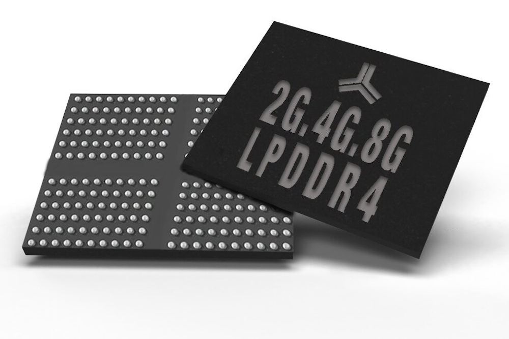
Alliance Memory 2Gb, 4Gb, and 8Gb LPDDR4 SDRAMs Offer Low Power Consumption to Increase Battery Life in Mobile Electronics; Devices Combine Low-Voltage Operation of 1.1V With Fast Clock Speeds of 1.6GHz for increased Efficiency and Performance
The 2Gb AS4C128M16MD4-062BAN, 4Gb AS4C256M16MD4-062BAN and AS4C128M32MD4-062BAN, and 8Gb AS4C256M32MD4-062BAN provide lower power consumption and faster speeds than the previous-generation LPDDR3 SDRAMs. The devices are available in 200-ball FBGA packages.
The devices offer low-voltage operation of 1.1V/1.8V to prolong battery life in portable electronics for the consumer and industrial markets. For higher efficiency for advanced audio and high-resolution video in embedded applications, the LPDDR4 SDRAMs provide clock speeds of up to 1.6GHz for high transfer rates of 3.2Gbps. For automotive applications, the AEC-Q100 qualified products can operate over an extended temperature range of -40°C to +105°C.
The LPDDR4 SDRAMs are organized as 1 channel (AS4C128M16MD4-062BAN and AS4C256M16MD4-062BAN) and 2 channels (AS4C128M32MD4-062BAN and AS4C256M32MD4-062BAN) per device. Individual channels consist of eight banks of 16 bits. The components feature fully synchronous operation; programmable read and write burst lengths of 16, 32, and on the fly; and selectable output drive strength. An integrated temperature sensor controls the self-refresh rate.
Alliance Memory’s LPDDR4 SDRAMs have been developed to provide a reliable drop-in, pin-for-pin-compatible replacement for numerous similar solutions in high-bandwidth, high-performance memory system applications — eliminating the need for costly redesigns and part requalification.
Key Specifications and Benefits:
On-chip ECC
AEC-Q100 qualified
Low-voltage operation of 1.1V/1.8V
Fast clock speeds of 1.6GHz
Extremely high transfer rates of 3.2Gbps
Automotive A2 Grade, temperature range -40°C to +105°C
Eight internal banks per channel
x32 for 2-channels per device (AS4C128M32MD4, AS4C256M32MD4)
x16 for 1-channel per device (AS4C128M16MD4, AS4C256M16MD4)
Programmable read and write latencies
Programmable and on-the-fly burst lengths (16 and 32)
Selectable output drive strength
On-chip temperature sensor to control self-refresh rate
Offered in the 200-ball FBGA package
Samples and production quantities of the new LPDDR4 SDRAMs are available now, with lead times of eight weeks.
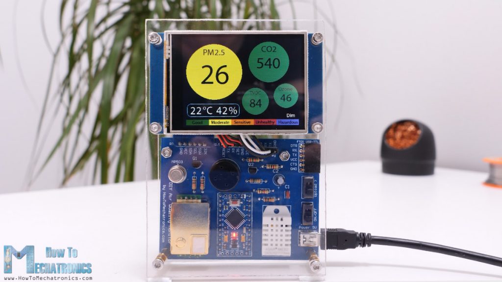
Dejan over at HowToMechatronics shared detailed instructions on how to build your own air quality monitor:
Have you ever wondered about the quality of the air you are breathing, or maybe, why you sometimes feel sleepy in the office or tired in the morning even after sleeping all night? Poor air quality can lead to many negative health effects as well as can cause tiredness, headaches, loss of concentration, increased heart rate and so on. Monitoring the quality of the air may actually be more important than you realize. So, in this tutorial we will learn how to build our own Air Quality Monitor which is capable of measuring PM2.5, CO2, VOC, Ozone, as well as temperature and humidity.
There are a lot of different LCD display interfaces depending on the requirements of resolutions, speed, cost, stability etc. The following outlines the common ones on the market:
Parallel vs Serial Interface
Parallel interface could transmit many data bits at the same time depending on the data bits width.
PROs: Simple
CONs: Need RAM, Speed is limited.
Serial interface could transmit just one-bit data at same time
PROs: less connection, hardware lower cost
CONs: Software is more complicated
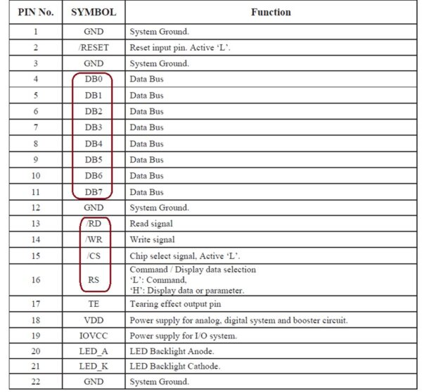
MCU Interface
MCU interfaces include two types, 6800 and 8080. 8080 is much more popular than 6800. Generally, MCU interface consist of 4/8/9/16bits data (like DB0, DB1, , , DB7; Note: 8bits is the most popular bits width), CS (chip select), RS (data register or instruction register select), RD (read enable), WR (write enable).
Used in Mono character, graphic, small TFT (smaller than 3.5”)
Fig. 1 MCU Parallel Interface
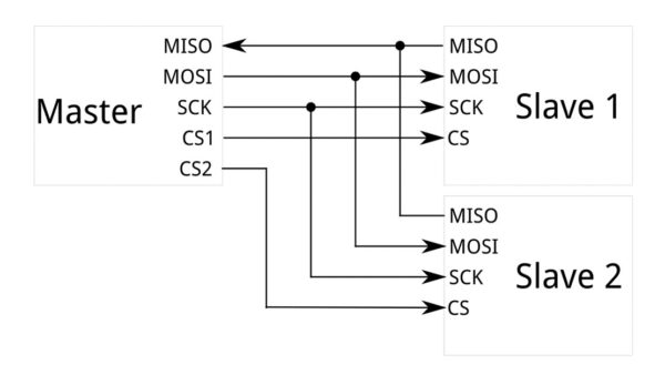
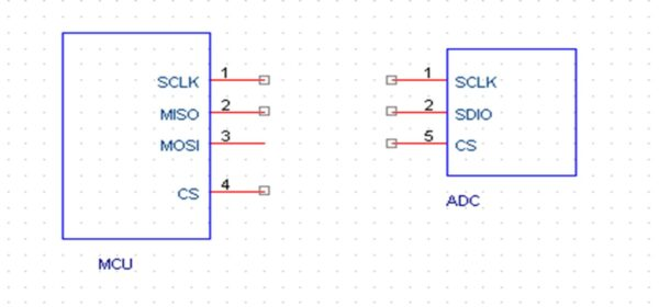
SPI Interface
SPI (Serial Peripheral Interface Bus) includes the following 4 wires:
SCLK: serial clock (output from master);
MOSI; master output, slave input (output from master);
MISO; master input, slave output (output from slave);
SS: slave select
Used in Mono digit, character, graphic LCD, small TFT, some CTP
Fig. 2, 4 Wire SPI Interface
Fig. 3, 3 Wire SPI Interface
IIC (I²C) Interface
I²C (Inter-Integrated Circuit) includes the following 2 connections.
SCL (serial clock wire),
SDA (serial data and address wire).
Used in Mono digit, character, graphic LCD, small TFT, most CTP
Fig. 4, IIC (I²C) Interface
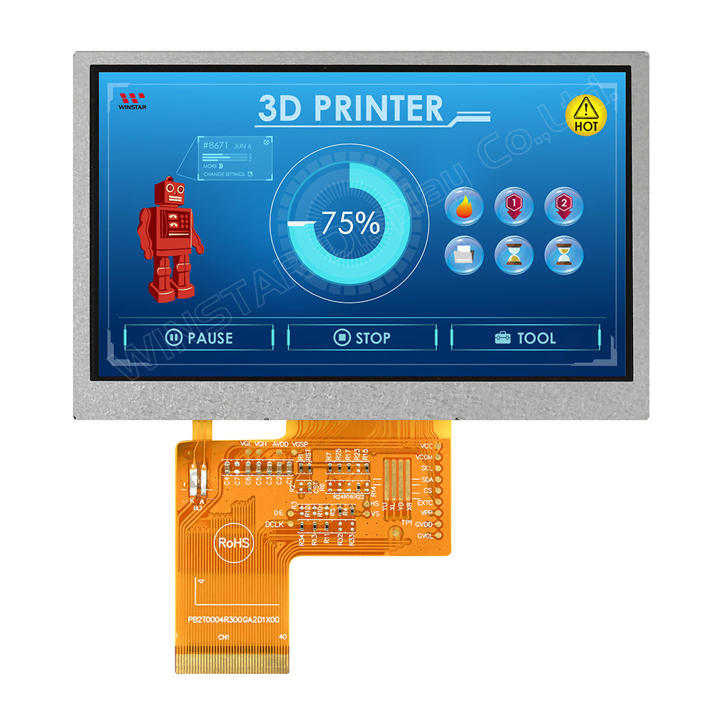
RGB Interface
RGB interfaces are often used to control large-scale high-resolution LCD displays. It includes 6/16/18bits data (like R0, R1, G0, G1, ,B0, B1, , ), VSYNC (Vertical synchronization), HSYNC (Horizontal synchronization).
Advantage is that R,G,B data is written to LCD directly without GRAM, high speed. Normally used in large-scale high-resolution LCD. No initialization code needed
Disadvantage is that controlling LCD is more complex, and requires more data wires than MCU interface.
Application: Medium size TFT (3.5” to 8”)
Fig.5 RGB interface includes 24 bit, 18 bit, 16 bit
Fig. 6 Examples of 24 Bit and 18 Bit RGB Interface
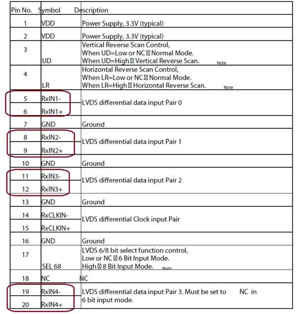
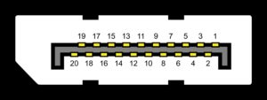
LVDS Interface
LVDS (Low-voltage differential signaling) is an electrical digital signaling standard that can run at very high speeds over inexpensive twisted-pair copper cables.
Most used in big panels (>7”)
Fig.7 Example of LVDS Interface
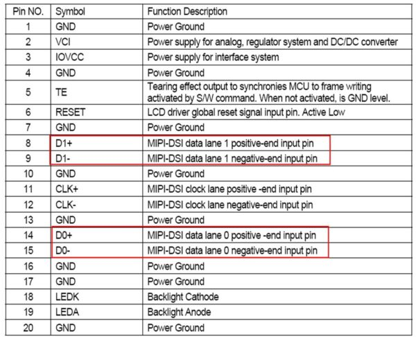
MIPI DSI Interface
MIPI (Mobile Industry Processor Interface) Alliance, DSI (Display Serial Interface)
Aimed at reducing the cost of display controllers in a mobile device. It is commonly targeted at LCD and similar display technologies. It defines a serial bus and a communication protocol between the host (source of the image data) and the device (destination of the image data)
MIPI Interface is getting more and more popular.
Fig. 8 An Example of MIPI Interface
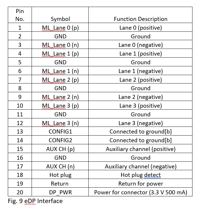
eDP interface
DisplayPort (DP) is a digital display interface developed by a consortium of PC and chip manufacturers and standardized by the Video Electronics Standards Association (VESA). The interface is primarily used to connect a video source to a display device such as a computer monitor, and it can also carry audio, USB, and other forms of data.
DisplayPort was designed to replace VGA, DVI, and FPD-Link. The interface is backward compatible with other interfaces, such as HDMI and DVI, through the use of either active or passive adapters. It is mostly used for larger size and higher resolution displays.
The above interfaces are basic LCD interfaces. They can be changed to other more human machine friendly interfaces. The examples are listed as below,
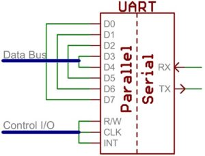
UART Interface
A universal asynchronous receiver/transmitter (UART) is a block of circuitry responsible for implementing serial communication. Essentially, the UART acts as an intermediary between parallel and serial interfaces. On one end of the UART is a bus of eight-or-so data lines (plus some control pins), on the other is the two serial wires – RX and TX.
Fig. 10 URAT Interface
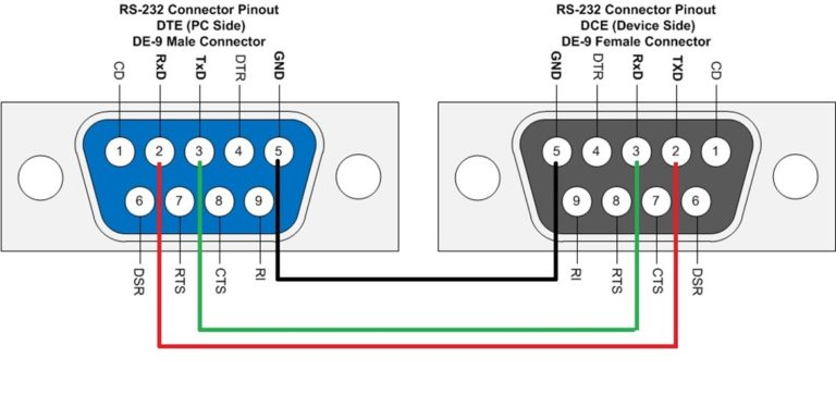
RS232
RS232 is a standard protocol used for serial communication, it is used for connecting computers and its peripheral devices to allow serial data exchange between them. As it obtains the voltage for the path used for the data exchange between the devices.
RS232 includes the following connections:
RX
VSS Signal Ground
Vdd +5v
Fig. 11 RS232 Interface
RS-232, when compared to later interfaces such as RS-422, RS-485 and Ethernet, has lower transmission speed, short maximum cable length, large voltage swing, large standard connectors, no multi point capability and limited multi drop capability. In modern personal computers, USB has displaced RS-232 from most of its peripheral interface roles. Few computers come equipped with RS-232 ports today, so one must use either an external USB-to-RS-232 converter or an internal expansion card with one or more serial ports to connect to RS-232 peripherals. Nevertheless, thanks to their simplicity and past ubiquity, RS-232 interfaces are still used—particularly in industrial machines, networking equipment, and scientific instruments where a short-range, point-to-point, low-speed wired data connection is fully adequate.
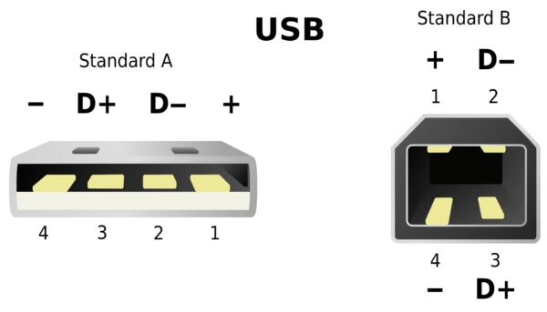
USB Interface
A Universal Serial Bus (USB) is a common interface that enables communication between devices and a host controller such as a personal computer (PC). It connects peripheral devices such as digital cameras, mice, keyboards, printers, scanners, media devices, external hard drives and flash drives. There have been four generations of USB specifications: USB 1.x, USB 2.0, USB 3.x and USB4.
It is widely used in capacitive touch panel connections.
Fig. 12 USB Interface
Some of the interfaces are interchangeable. For further information, please consult Orient Display technical support team.
Author Bio
This article is an original piece of content written by Bill Cheung, a marketing manager who has an engineering and technical support background at Orient Display. We are a LCD and display technology provider with over two decades of industry experience in delivering cutting edge display solutions. Please browse our knowledge base if you would like to learn more about LCDs!
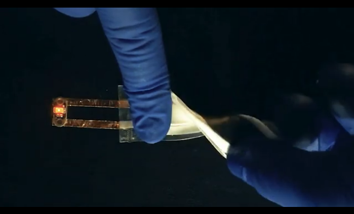
A team of researchers made up from the University of California San Diego and California-based company ZPower have developed a flexible, rechargeable silver oxide-zinc battery with a 5 to 10 times greater energy density than standard batteries. A good characteristic of the battery is that it is easier to manufacture because most flexible batteries need to be manufactured in sterile conditions, under vacuum, but this new battery can be screen printed in normal lab conditions. The device can be applied in flexible, stretchable electronics for wearable as well as soft robotics. About the battery, Lu Yin, one of the paper’s co-first authors and a Ph.D. student in the research group of UC San Diego’s nanoengineering Professor Joseph Wang says:
“Our batteries can be designed around electronics, instead of electronics needed to be designed around batteries.” He continues “The areal capacity for this innovative battery is 50 milliamps per square centimeter at room temperature—this is 10-20 times greater than the areal capacity of a typical Lithium ion battery. So for the same surface area, the battery described in Joule can provide 5 to 10 times more power. This kind of areal capacity has never been obtained before, and our manufacturing method is affordable and scalable.”
The new battery offers higher capacity than any of the flexible batteries currently available on the market thanks to its much lower impedance—the resistance of an electric circuit or device to alternative current. The lower the impedance, the better the battery performance against high current discharge. About future usage, Jonathan Scharf the paper’s co-first author says:
“As the 5G and Internet of Things (IoT) market grows rapidly, this battery that outperforms commercial products in high current wireless devices will likely be a main contender as the next-generation power source for consumer electronics.”
In their series of test, the batteries successfully powered a flexible display system equipped with a microcontroller and Bluetooth modules, and also performed better than commercially available Li coin cells. The battery is very durable, its cells were recharged for more than 80 cycles, without showing any major signs of capacity loss. The cells also remained functional in spite of repeated bending and twisting. The battery was created via a proprietary cathode design and chemistry from ZPower. Wang and his team combined their expertise in printable, stretchable sensors and stretchable batteries to create this battery. Meng and her colleagues also offers their expertise in advanced characterization for electrochemical energy storage systems and characterized each iteration of the battery prototype until it reached peak performance.
The battery’s exceptional energy density is as a result of its silver oxide-zinc, (AgO-Zn) chemistry. Conventional commercial flexible batteries utilize a Ag2O-Zn chemistry, as a result they usually have limited cycle life and have low capacity. This limits their use to low-power, disposable electronics. AgO is traditionally considered unstable. However, ZPower’s AgO cathode material depends on a proprietary lead oxide coating to improve AgO’s electrochemical stability and conductivity. As an added advantage, the AgO-Zn chemistry is responsible for the battery’s low impedance. The battery’s printed current collectors also offer excellent conductivity, which also enables it achieve lower impedance.
The batteries are printed onto a polymer film that is chemically stable, elastic and has a high melting point (about 200 degrees C or 400 degrees Fahrenheit) that can be heat sealed. The current collectors, the zinc anode, the AgO cathode and their corresponding separators each comprise of a stacked screen-printed layer. The team is already working on the next generation of the battery, aiming for cheaper, faster charging devices with even lower impedance that would be used in 5G devices and soft robotics that require high power and customizable and flexible form factors. You can read more about the project here.
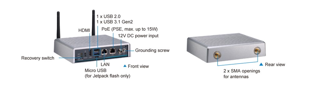
Axiomtek – a world-renowned leader relentlessly devoted in the research, development and manufacture of series of innovative and reliable industrial computer products of high efficiency – is pleased to announce the AIE100-903-FL-NX, its ultra-compact and state-of-the-art edge AI system. The high-performance AIE100-903-FL-NX is powered by the NVIDIA® Jetson Xavier™ NX module which has a powerful 6-core NVIDIA® Carmel ARM® v8.2 64-bit processor and 384-core NVIDIA® Volta™ GPU architecture with 48 Tensor cores; in addition, it integrates Allxon Device Management Solutions (Allxon DMS) to provide a cost-effective and simplified device management solution with comprehensive remote management capabilities. The AIE100-903-FL-NX is ideal for smart city, smart manufacturing, smart retail, and other intelligent edge AI applications.
“The AIE100-903-FL-NX is a waterproof, fanless NVIDIA-based AI edge inference system designed for AI computing and deep learning applications, such as behavior analytics, face recognition and vehicle analysis. Due to its rugged design, the ultra-compact edge computing device can operate in harsh environments with a wide range of temperatures from -30°C to +50°C and can withstand vibration up to 3 Grms. In addition, it offers an optional waterproof IP42-rated cover kit for enhanced protection in semi-outdoor environments,” said Annie Fu, the product manager of Product PM Division at Axiomtek. “Besides the outstanding hardware solutions, the AI-powered AIE100-903-FL-NX is integrated with cloud-based Allxon DMS to provide remote management for convenient real-time control on devices. Allxon DMS offers rapid deployment and integration on multiple operating systems, reduces system downtime and maintenance costs, and further provides a wide breadth of centralized cloud device management. This industrial edge AI system is the best choice to simplify the large-scale deployment of AIoT platforms.”
The AIE100-903-FL-NX offers support for NVIDIA® JetPack 4.4 for ease of development in AI computing and deep learning applications. It has abundant I/O connectivity, including one USB 3.1 Gen2 port, one USB 2.0 port, one Micro USB port, one GbE LAN port, one GbE PoE port and one HDMI 2.0 port supporting 4K2K. It also has one recovery switch, one reset button, one power button, one 12V DC power input and two SMA-type antenna openings. Users can use the recovery switch and Micro USB to easily flash the image without opening the chassis. The AIE100-903-FL-NX has a 16GB eMMC onboard and is equipped with one M.2 Key M 2280 SSD slot with PCIe x4 NVMe and one Micro SD slot for real-time massive workload processing at the edge. Furthermore, the AIE100-903-FL-NX has one full-size PCIe Mini Card slot supporting USB and PCIe signal and one SIM slot for 3G/4G, GPS, Wi-Fi and Bluetooth connections.
Advanced Features:
NVIDIA® Jetson Xavier™ NX with Volta™ GPU architecture with 384 NVIDIA CUDA® cores
High AI computing performance for GPU-accelerated processing
Ideal for edge AI smart city applications
Supports one 15W GbE PoE for a camera
Wide operating temperature settings ranging from -30°C to +50°C
Axiomtek’s AI-powered AIE100-903-FL-NX is now available for purchase. For more product information or customization services, please visit our global website at www.axiomtek.com or contact one of our sales representatives at info@axiomtek.com.tw.
Texas Instruments’ driver features integrated current sense, 1/256 microstepping, STEP/DIR interface, and smart tune technology
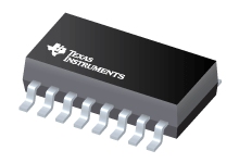
Texas Instruments’ DRV8428 is a stepper motor driver for industrial and consumer applications. The device is fully integrated with two N-channel power MOSFET H-bridge drivers, a microstepping indexer, and integrated current sensing. The DRV8428 can drive up to 1 A full-scale output current (dependent on PCB design).The DRV8428 uses internal current sense architecture to eliminate the need for two external power sense resistors, saving PCB area and system cost. The device uses an internal PWM current regulation scheme selectable between smart tune and mixed decay options. Smart tune automatically adjusts for optimal current regulation, compensates for motor variation and aging effects, and reduces audible noise from the motor.
The simple STEP/DIR interface allows an external controller to manage the direction and step rate of the stepper motor. The device can be configured in different step modes ranging from full-step to 1/256 microstepping. A low-power sleep mode is provided for very low standby quiescent standby current using a dedicated nSLEEP pin. Protection features are provided for supply undervoltage, overcurrent, short circuits, and overtemperature. Fault conditions are indicated by the EN/nFAULT pin.
Features
PWM microstepping stepper motor driver:
Simple STEP/DIR interface
Microstepping indexer: up to 1/256
Integrated current sense functionality:
No sense resistors required
Full-scale current accuracy: ±6%
Smart tune decay technology and mixed decay options
Operating supply voltage range: 4.2 V to 33 V
RDS(ON): 1,500 mΩ HS + LS at 24 V, +25°C
Current capacity per bridge: 1.7 A peak, 1 A full-scale, 0.7 ARMS
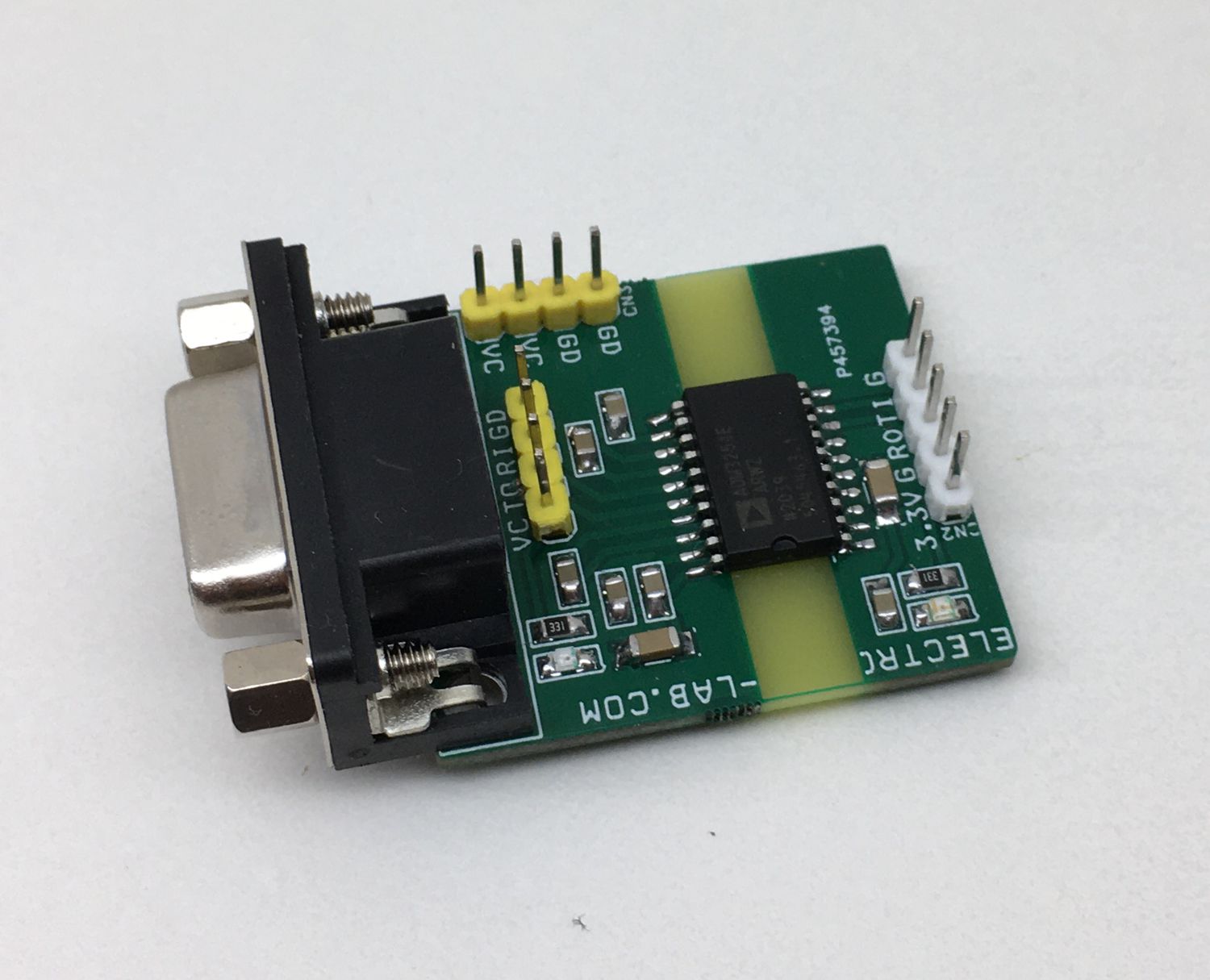
The project presented here provides an isolated interface between the RS-232 cable network and the connected UART systems to protect against voltage spikes and ground loops within the noisy environment and improve system reliability. The project achieves a robust data communication link in harsh industrial environment. ADM3251E chip from Analog Devices is the heart of the project, this chip is a high speed, 2.5KV fully isolated, single-channel RS-232 transceiver device that operates from a single 5 V power supply. Due to the high ESD protection on the RIN and TOUT pins, the device is ideally suited for operation in electrically harsh environments or where RS-232 cables are frequently being plugged and unplugged. Four external 0.1 μF charge pump capacitors are used for the voltage doubler/inverter, permitting operation from a single 5 V supply. Project operates at data rates up to 460kbps. RS-232 transceiver D-Sub 9 Pin Female block provide convenient signal connections. D2 Power LEDs on respective isolation ends. The chip has inbuilt isolated DC-DC Converter thus the project can work with single supply. Apply 5V DC to CN2 and project is ready to go.
Isolated, Single-Channel RS232 transceiver (Isolated RS232 to UART) – [Link]
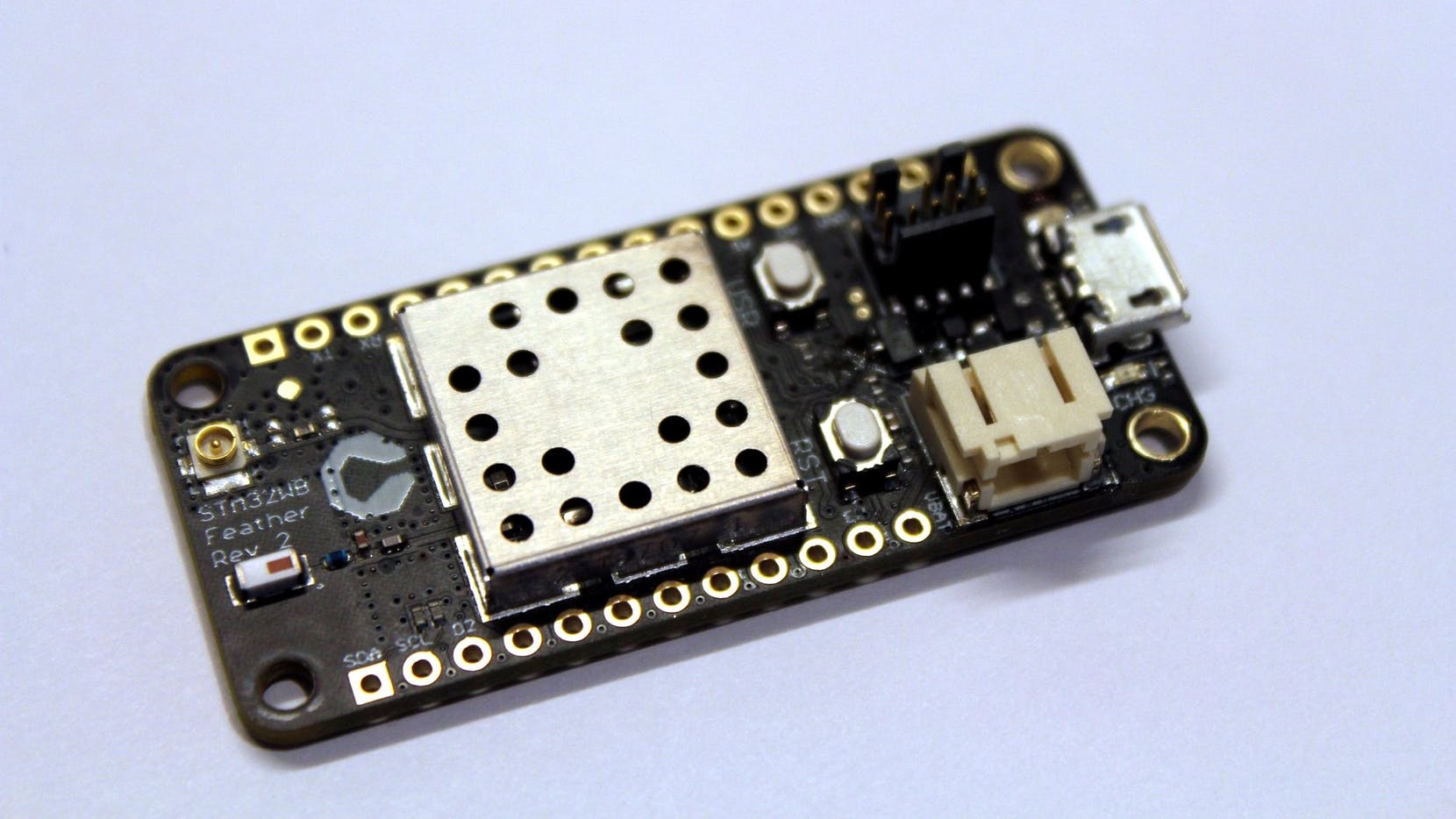
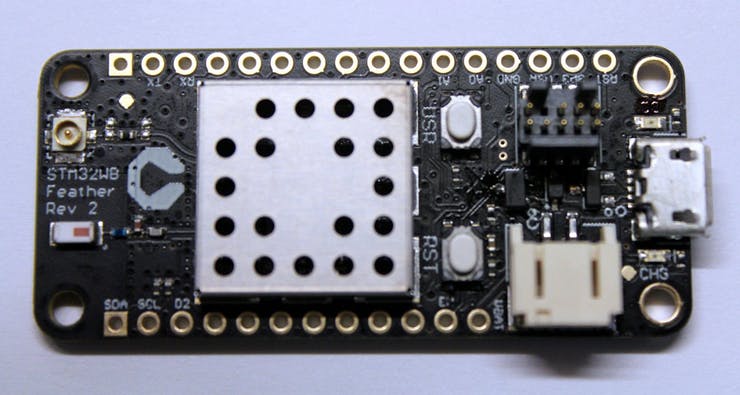
Reclaimer Labs has launched an STM32WB Feather development board that is based on STMicro’s first wireless STM32 MCU which was announced sometime around last year.
The STM32WB Feather board like other development boards in the STM32 family of wireless MCUs is built around the STM32WB55CG SoC which includes an 64MHz Arm Cortex‐M4 running as the main processor along with a 32MHz Cortex‐M0+ as a co-processor for Bluetooth.
The STM32WB Feather board in Adafruit feather standard, has an STM32WBCGU6 Bluetooth SoC at its core alongside other wireless and ultra-low-power features. One advantage this new line of IoT SoC has over others is that of size and space. The chipset integrates everything together into a single chip, so there’s no need for separate chips for microcontroller and radio. It can also achieve lower power sleep states thus making the board efficient at low power.
The chipset has 1MB of flash memory that is shared between the main and co-processors, a USB ROM bootloader, and 256kB of SRAM, while the board itself is equipped with an on-board chip antenna that radiates high – frequency electromagnetic waves, a wide variety of I/O, including 6x analog input pins, UART, I2C, and SPI, plus 7x digital GPIO pins.
The STM32WB Feather board also possesses embedded security hardware functions like 256-bit AES hardware encryption, PCROP read/write protection, JTAG fuse, and public-key cryptography with an elliptic curve encryption engine.
Here’s a list of some of the features and specifications that the board has:
STMicro STM32WB55CG Bluetooth SoC with:
Arm Cortex-M4 application core
Arm Cortex-M0+ Bluetooth co-processor
256 KB SRAM
1 MB Flash storage (shared between main and co processors)
USB ROM Bootloader
128 Mbit external SPI NOR Flash memory
On-board chip antenna
u.Fl connector for external antenna
16-pin plus 12-pin unpopulated headers with 6x analog input pins
UART, I2C, SPI, plus 7x GPIO pins
1x Standard SWD debug connector
1x User button and LED
32.768 kHz crystal for LSE/RTC
5V power supply via micro USB port
2-pin battery header, and,
LiPo battery charger
Dimensions: Adafruit feather form factor
The company has made things easier for users by providing an example project using the STM32CubeIDE, since the STM32WB Feather Board can be programmed with STM32CubeProgrammer.
The board is currently available and sells on Tindle for just $45, in case you’re interested in purchasing one, but further details on it including a full schematic and a link to the code sample can be found on the Reclaimer Labs’ website.
GNSS location with standards like GPS is a key feature of smartphones and other devices. They enable you navigate around, and share your location with friends, family, and business contacts. However, sometimes we find it difficult to get an accurate location because of a number of factors like tall buildings in urban area bouncing the satellite network, etc. This can be really problematic for someone seeking for directions, delivery companies, e-hailing taxi riders etc. However, Google has come up with a solution on android devices via 3D mapping aided GPS corrections.
For reasons behind the project, they say:
“At Android, we want to make it as easy as possible for developers to create the most helpful apps for their users. That’s why we aim to provide the best location experience with our APIs like the Fused Location Provider API (FLP). However, we’ve heard from many of you that the biggest location issue is inaccuracy in dense urban areas, such as wrong-side-of-the-street and even wrong-city-block errors. This is particularly critical for the most used location apps, such as rideshare and navigation. For instance, when users request a rideshare vehicle in a city, apps cannot easily locate them because of the GPS errors. The last great unsolved GPS problem. This wrong-side-of-the-street position error is caused by reflected GPS signals in cities, and we embarked on an ambitious project to help solve this great problem in GPS.”
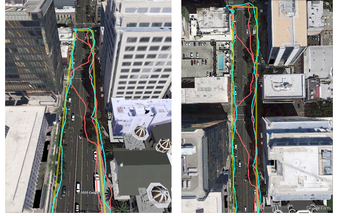
Picture of a pedestrian test, with Pixel 5 phone, walking along one side of the street, then the other. Yellow = Path followed, Red = without 3D mapping aided corrections, Blue = with 3D mapping aided corrections.
Explaining how the 3D mapping works, Google says:
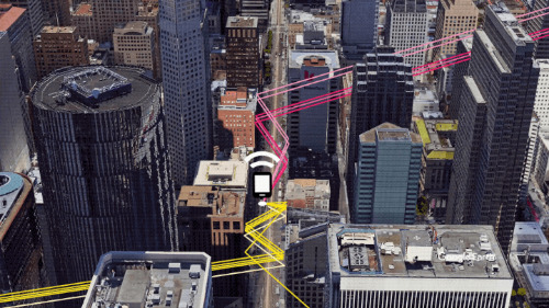
“The 3D mapping aided corrections module, in Google Play services, includes tiles of 3D building models that Google has for more than 3850 cities around the world. Google Play services 3D mapping aided corrections currently supports pedestrian use-cases only. When you use your device’s GPS while walking, Android’s Activity Recognition API will recognize that you are a pedestrian, and if you are in one of the 3850+ cities, tiles with 3D models will be downloaded and cached on the phone for that city. Cache size is approximately 20MB, which is about the same size as 6 photographs. Inside the module, the 3D mapping aided corrections algorithms solve the chicken-and-egg problem, which is: if the GPS position is not in the right place, then how do you know which buildings are blocking or reflecting the signals? Having solved this problem, 3D mapping aided corrections provide a set of corrected positions to the FLP. A system API then provides this information to the GPS chip to help the chip improve the accuracy of the next GPS fix.”
Android’s 3D mapping aided corrections automatically works when the GPS is being used by a pedestrian in any of the 3850+ cities, on any phone that runs Android 8 or later. The best way for developers to take advantage of the improvement is to use FLP to get location information. The further 3D mapping aided corrections in the GPS chip are available to Pixel 5 and Pixel 4a (5G) today, and will be rolled out to the rest of the Android ecosystem (Android 8 or later) in the next several weeks. We will also soon support more modes including driving.
Android’s 3D mapping aided corrections cover more than 3850 cities, including:
North America: All major cities in USA, Canada, Mexico.
Europe: All major cities. (100%, except Russia & Ukraine)
Asia: All major cities in Japan and Taiwan.
Rest of the world: All major cities in Brazil, Argentina, Australia, New Zealand, and South Africa.
About release, Google says:
“With this December Pixel feature drop, we are releasing version 2 of 3D mapping aided corrections on Pixel 5 and Pixel 4a (5G). This reduces wrong-side-of-street occurrences by approximately 75%. Other Android phones, using Android 8 or later, have version 1 implemented in the FLP, which reduces wrong-side-of-street occurrences by approximately 50%. Version 2 will be available to the entire Android ecosystem (Android 8 or later) in early 2021.” You can read more about the 3D mapping here.
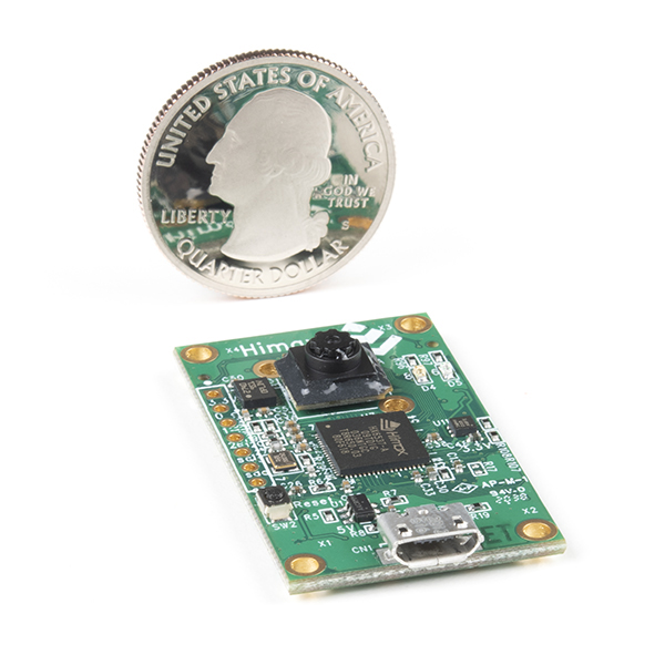
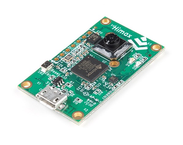
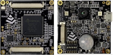
If you are looking for an AI development board that supports TensorFlow Lite for microcontrollers, then Himax has something that might interest you. This board claims to be the perfect solution for your machine vision and AI/ML based applications as it has support for TFLite. There are many existing AI development boards which are in the feather form factor like QuickFeather development board or even RISC-V based EdgeX AI Kit which are interesting but quite expensive when compared to Himax AI development board for microcontrollers.
The AI development board is powered by HX6537-A SoC based on ARCv2DSP instruction set architecture that comes with a 32-bit ARC processor from Synopsys that is “optimized for sensor fusion, voice detection, speech recognition and audio processing that are common in Internet of Things (IoT) and other embedded applications.” The SoC supports embedded 2MB SRAM for code and data memory along with 2MB flash memory. It also “features a power-efficient unified 32×32 MUL/MAC unit and support for fixed-point DSP data types and vector/SIMD (single instruction multiple data) operations.”
The company says,
“This new WE-I Plus EVB board is optimized for TensorFlow Lite for Microcontrollers target applications, and it integrates AoS™ VGA camera, L/R microphones, 3-axis accelerometer, and USB to SPI/I2C/UART bridge into one board with 40mmx27mm dimension. It is the best leading ultralow power and performance solution for TensorFlow Lite for Microcontrollers applications in this industry.”
Specifications
SoC: WE-I Plus Application Specific Integrated Circuit (HX6537-A)
ARC 32-bit EM9D DSP with FPU clocked up to 400 MHz
2MB SRAM
2MB Flash
Onboard Camera: Himax HM0360 AoS TM ultra-low power VGA camera with 1.6″ CMOS Sensor along with resolution of 640 x 480 pixels at 60 frames per second.
USB Bridge: FTDI USB connectivity to devices with a SPI/I2C/UART interface
Power supply: 3.3/2.8/1.8/1.2V
Expansion header
1x I2C port
3x GPIOs
Power/Ground
According to the manufacturer,
“To support “Voice” applications, this board features two MEMS microphones. The latency time of the 20KB TensorFlow Lite for Microcontrollers “Micro speech” example is only 6ms. To support “Vibration” applications, this board features a STM LSM9DS1 IMU for 3-axis accelerometer function. The WE-I Plus features an ASIC embedded EM9D DSP Floating-Point-Unit (FPU).”
How to get started?
To get started with the development board, you will need expert coding skills that will help you code the development board. You will also need a SDK.AI, which is a collaboration with Google TFL micro & Synopsys MLI teams along with TensorFlow Lite for microcontrollers that is designed to run machine learning models on microcontrollers. For more information, you can visit the product page on Himax’s website.
For interested folks, the board is available to buy via SparkFun for just $65 which is very less compared to many existing AI development boards in the market like EdgeX AI Kit.