Hall Effect switches have self-diagnostics capability

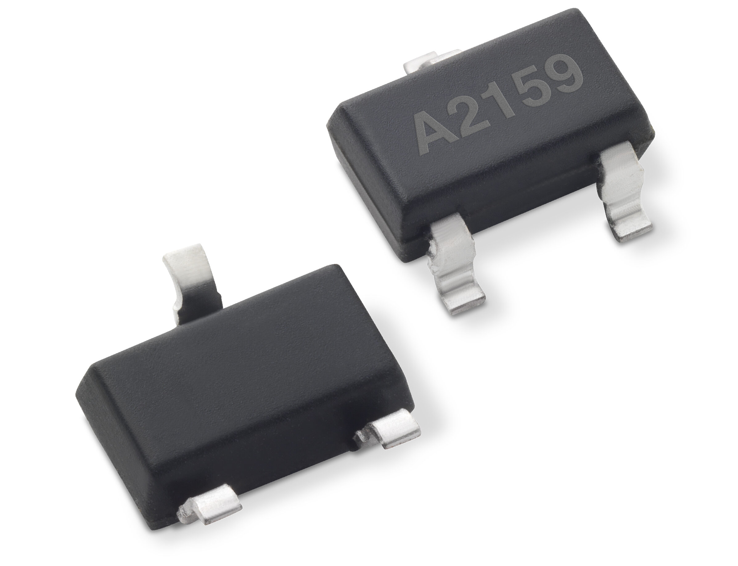
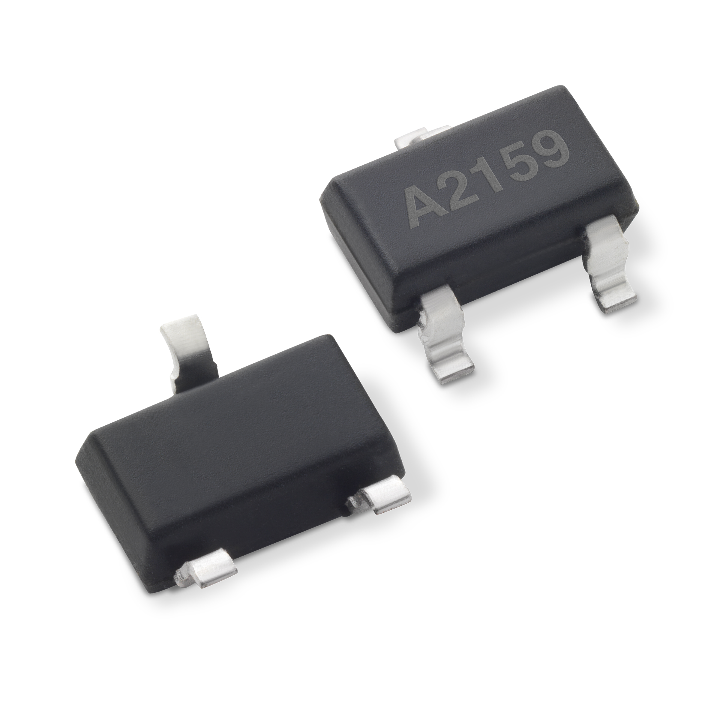
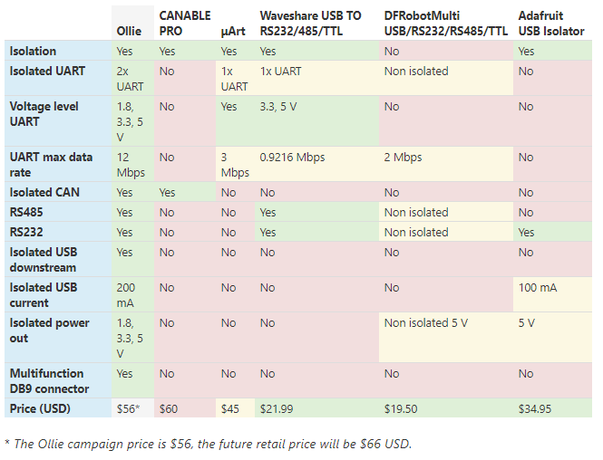
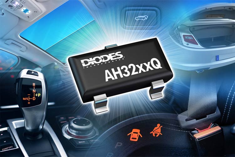
Diodes Incorporated has announced a family of automotive-compliant, two-wire unipolar (AH323xQ/4xQ) and latch (AH327xQ/8xQ) switch integrated circuits (ICs) that provide high sensitivity and high stability over wide operating voltage and temperature ranges. The ICs are for use in automotive proximity- and position-sensing applications, including seatbelt buckle, power window, gear selector and seat position. The adoption of two-wire hall switches reduces the number of wires required in the harness, saving on system complexity and cost while improving robustness to electrical noise.

The AH324xQ and AH328xQ have integrated self-diagnostics which continually monitor the main device blocks, supply voltage, and temperature. There is a third output state that warns of an abnormal condition. These devices are ISO 26262 ASIL-B ready, having been developed using rigorous design processes with safety analysis conducted in accordance with the ISO 26262 standard.

Diodes adopted an advanced chopper-stabilized design, which provides superior stability of the magnetic operating and releases points (BOP/BRP) over the 2.7V to 27V operating voltage and -40˚C to +150˚C temperature range. This stability, coupled with a high ESD rating of 8kV, built-in reverse blocking diode, and supply pin Zener clamp, enables the AH32xxQ series to meet the demanding requirements of automotive proximity/position-sensing applications.

All AH32xxQ devices are supplied in the SC59 package. They are qualified to AEC-Q100, manufactured in IATF 16949 certified facilities, and support PPAP documentation. The AH324xQ and AH328xQ have a unit price starting at $0.40 in 3000 piece quantities, while the AH323xQ and AH327xQ start at $0.36 in 3000 piece quantities.

more information: https://www.diodes.com

High Sensitivity Ultra-Low Power Tunneling Magnetoresistance TMR Switch

Littelfuse’s TMR is a magnetically-triggered digital switch with high sensitivity and ultra-low power consumption

Littelfuse’s TMR switch is a digital magnetic switch that integrates tunneling magnetoresistance (TMR) and CMOS technology to provide a magnetically-triggered digital switch with high sensitivity and ultra-low power consumption. The TMR switch contains a magnetic sensor and CMOS signal processing circuitry with an on-chip TMR voltage generator for precise magnetic sensing. A TMR voltage amplifier and comparator plus a Schmitt trigger provide switching hysteresis for noise rejection and a bandgap regulator is used to provide a temperature compensated supply voltage for internal circuits.

Features
  • TMR technology supports operating point thresholds from 4 Gauss to 35 Gauss
  • Ultra-low power consumption: 200 nA
  • Operation with north and south pole / X-axis or Z-axis sensing direction
  • Available in uni-polar, omni-polar, and bi-polar (latching) operating modes
  • Output type: push-pull or open-drain
Applications
  • Proximity detection
  • Utility meters including gas, water, and heat meters
  • Position and speed sensing
  • Rotary sensing
  • Motor and fan control
  • Solid-state switches

more information: https://www.littelfuse.com/products/magnetic-sensors-and-reed-switches/tmr-magnetic-ic/tmr-switch/lf11115tmr.aspx

The Launchpad – A $2 Arduino Nano alternative

Boards like the Arduino and Raspberry Pi have their origins, deep in education, either maker education as a way for people to express themselves (Arduino) or an affordable and portable way for people to learn about computers and programming (Raspberry Pi). The culture of creating solutions targetted at beginners, is one that is quickly fading in the ecosystem, as most of the boards or project we review in recent times are power-up boards, focussed or more useful to advanced users.

While catering for advanced users is important, we believe there is room for both and are glad to see someone else thinking and building something along that line. Meet the Launchpad; A 2$ development board targeted at helping newbies get into programming and making.

Designed by Hackaday user, Clyde D. Corpus, the Launchpad is a tiny Arduino compatible microcontroller development board that does away with the “probably overused” ATmega328p used in the classic Arduino boards in favor of a newer, cheaper, and equally capable ATtiny1616 microcontroller. Ah yes, Launchpad is the name of a board by Texas Instruments. It was one of the few things Clyde discovered late and we should be getting a new name for the board when it’s ready to go into sales.

Sharing on the motivation behind the board on his Hackaday post, Clyde noted that:

“The goal is to design a board aimed at basic education that can be made for as low as $2”, and this component cost was achieved, leading to the emergence of the current version which in comparison has all the features of the classic Arduino Nano, a faster 20MHz clock speed, true analog output, but with smaller IO pins.

Some highlight features of the first version of the board include:

  • Breadboard-friendly pinout
  • Micro USB  type B connector
  • Microchip ATtiny1616
    • 20MHz clock speed
    • 16kB of flash memory
    • 2kb of RAM
    • 256 bytes of EEPROM
    • 18 I/O pins (1 is currently configured as the reset pin)
    • 8 PWM outputs (8-bit resolution)
    • 12 analog inputs (10-bit resolution)
    • 1 true analog output (0 – 4.3V)
    • UPDI programming interface
    • 1 UART
    • 1 SPI
    • 1 I2C
    • Configurable custom logic (CCL) pins
    • tinyAVR 1-series architecture (similar to the megaAVR 0-series chips on the Arduino Nano Every and Uno WiFi rev2 boards)
  • OptibootX bootloader
  • CH340G USB to serial converter
  • AMS1117 5V LDO voltage regulator

The development of the board itself has been quite the learning curve for Clyde as documented on Hackaday, and we are hoping he infuses the lessons learned into the board so it’s easy for others to walk his path.

The board is not yet available for sale, but you can follow the project on Hackaday to learn more about the board and its development.

Aledia – Pioneering nanowire microLED’s on 300 mm Wafers

We talk a lot about downsizing. It is, and always will be on the top priority list of the world of electronics. Without smaller sizes, we would never have gotten to this state, where our projects can be housed in a small PCB and ran on an ATTiny mcu. It is one of the most fascinating things about this area, seeing how much you can cram into a small space. Today, we have something among those lines, not necessarily about high performance in small sizes, but the microLED display technology, which the company Aledia is pushing further.

So, you probably heard about the MicroLED technology, but if you did not, here is a small refresher: it is a new display technology based on GaN (Gallium Nitride) that offers more than what we have nowadays with OLED and LCD. It presents more durability than OLED, delivering those perfect dark colors with no danger of burn-in after a long time, it can be brighter than any other technology on the market, with better color quality, faster display switching speeds, and better energy efficiency.

LEDs and MicroLEDs through the microscope

Even though it has already caught the eye of TV manufacturers and co., it still is not a sounding name on the market, alongside, for example, OLED, but why? Being a new technology, its manufacturing process is still a bit blurry, with companies such as Aledia trying to find the best way to enable the mass production that will allow the technology to strive on the market. As such, Aledia came through with the world’s first MicroLED production on 300 mm silicon wafers, which only has been done on 200 mm wafers to this point. The larger wafer size means lower transfer and assembly costs.

To analyze the issue with producing larger wafers, we must take a look at its production process. Planar or “2D” microLEDs are produced by depositing flat layers of GaN, mainly on small 100mm sapphire wafers, due to the stress seen on the microLEDs when the wafer size is increased. With “3D” microLED technology, developed by them, this fabrication process can be performed in bigger and silicon wafers, meaning the silicon foundries can aid in their production.

The Wall: a modular MicroLED TV from Samsung

Having these two breakthroughs combined together, is there some hope to see this technology soon in our everyday lives? Well, the use of larger silicon wafers and making use of the silicon foundries to provide the high demands of the industry are two steps in the right direction. But, there is a need of around 24 million 300 mm wafers per year. Will we see it any time soon? Only time will tell, but one can hope.

Aledia company link: https://www.aledia.com/en

Hackboard 2 Intel Gemini Lake Based SBC Features Windows 10 Pro

Hackboard, a Texas-based startup has launched a campaign on Crowdsupply for Hackboard 2, which is a new single-board computer (SBC) designed from the ground up to be one of the most powerful and affordable Windows-capable, Intel-based computers ever. The SBC features optional 4G or 5G connectivity, and it is ideal for students, teachers, families, makers, and hobbyists alike. Unlike the Raspberry Pi, Hackboard 2 is based on a powerful Intel processor capable of running Windows, and unlike other Intel-based SBCs, Hackboard 2 is incredibly affordable. The Hackboard 2 features a dual-core 1.1GHz/2.8GHz Celeron N4020, with a 6W TDP from the second wave of Gemini Lake RefreshSoCs. The SBC also ships with 4GB DDR4 and 64GB eMMC and provides M.2 B- and B/M-key slots. For low-power expansion, the SBC features a 40-pin GPIO header which is compatible with Raspberry Pi HATs. Python is pre-installed for hacking the GPIO. The board also features a GbE port, 802.11ac with Bluetooth 5.1, and 3x USB 3.0 ports.

Hackboard 2 is a reliable, high-performance platform that is well suited to a large and diverse set of possible projects. Application of the Hackboard 2 includes:

  • Entertainment systems like media servers, game consoles, and digital audio hubs
  • Home automation controllers and smart-home peripherals like IoT appliances and security systems
  • Sensor gateways such as industrial monitors and controls


The standard version of Hackboard 2 features preinstalled Windows 10 Pro, a full-featured version of Windows that retails for more than the price of Hackboard 2 itself, and also comes preinstalled with the powerful Python programming language for accessing Hackboard 2’s GPIO.

There is a limited edition version of Hackboard 2, which is preinstalled with Ubuntu Linux and it will be available only during the Crowd Supply campaign. The hardware is identical, but it features Linux instead of Windows. The Hackboard 2 Starter Kit features everything you need to hook up Hackboard 2 to your own monitor or TV and be productive right away. It includes a Hackboard 2 with Windows 10 Pro, a 12 VDC / 3 A international power supply, a heatsink, two board-mountable antennas, a protective ABS plastic case, a 1080p USB 2 video camera, and a wireless keyboard with integrated trackpad, all slim and lightweight enough to take on the go. Optional 4G and 5G cellular modems are available separately.

The Hackboard 2 Complete Kit features everything you need to carry out your work right away. It includes everything that comes with a Hackboard 2 Starter Kit, plus a portable 13.3″ IPS 1080p HD display with integrated speakers, USB C and HDMI inputs, a mini USB B power supply (5 V / 3 A), and a protective cover that doubles as a stand, all slim and lightweight enough to take on the go. Optional 4G and 5G cellular modems are available separately.

Features & Specifications:

  • Processor – Intel Celeron N4020
    -Dual-core, 64-bit
    -Up to 2.8 GHz clock
    -4 MB cache
  • Memory & Storage
    -4 GB DDR4 RAM
    -64 GB onboard eMMC flash
    -Two NVMe M.2 slots accommodate up to 4 TB additional storage
  • Video & Audio
    -Intel UHD Graphics 600
    -4K HDMI 2.1 output
    -30-pin eDP 11.6″-15.6″ screen connector
    -6-pin touchscreen interface
    -3.5 mm CTIA audio jack (stereo + mic)
    -5-pin stereo speaker connector
  • Connectivity
    -Wi-Fi – Intel dual-band AC95060 rated at 1.73 Gb/s
    -Bluetooth 5.1
    -Gigabit Ethernet
    -Optional 4G or 5G cellular modem
  • Expandability
    -3 x USB 3.0 ports
    -5-pin USB 2 camera connection
    -40-pin GPIO header (RPi-HAT-compatible with pass-through adapter)
    -NVMe M.2 B key slot
    -NVMe M.2 B & M key slot
  • Power – included
    -12 VDC, 3 A international power supply
    -10-pin 3.7 V rechargeable battery input connector
    -Heatsink
    -Small cell battery for up to two years BIOS backup
  • Dimensions
    -120 mm x 80 mm
    -Corner mounting holes centered 5 mm from edges
Hackboard 2 with two included antennas

The Hackboard 2 is available on Crowd Supply till Jan. 15, with pricing starting at $99 with Ubuntu, and $140 with Win 10 Pro. Shipments are due April 30, 2021, with shipping costing $8 in the US and $20 to other parts of the world. You can find more information on Hackboard’s announcement and on the Hackboard 2 Crowd Supply page and the Hackboard website.

ESP32-M1 Reach Out is a compact and richly-featured ESP32-M1 dev board with up to 1.2 km Wi-Fi range

Bison Science is preparing to launch a project that aims to be a perfect solution to the Wi-Fi range limitations of existing boards, called the ESP32-M1 Reach Out Development Board.

The ESP32-M1 Reach Out development board is said to increase range up to two to three times, and is quoted to be more than 1.2km. The ESP32-M1 Reach Out is an excellent solution for developers, makers, engineers, and hobbyists who seek to develop robust communication systems using Wi-Fi and Bluetooth protocols even at a distance. It is integrated with an ESP32 RF SoC that makes getting going with long-range RF as simple as can be. The chipset features both a microcontroller and RF stage in a single package and guarantees a range of more than 1.2km using Wi-Fi 802.11b.

Though with a small size, the ESP32-M1 Reach Out has a methodical design that features amongst others, 17 GPIOS, 3 different voltage outputs, digital external interfaces, external antenna connectors, and a high-power radio front-end for Wi-Fi.

Features & Specifications of the ESP32-M1 Reach Out Development Board include:

  • SoC: ESP32-D0WDQ6 RF clocked up to the frequency of 240MHz
  • 32 Mbit flash memory
  • CP2102 USB serial bridge (USB to UART converter)
  • Wi-Fi 802.11 b/g/n
  • Bluetooth 4.2 and Bluetooth Low Energy
  • Digital external interfaces and external antenna ports for Wi-Fi and Bluetooth
  • Qorvo QPF4219 PA and LNA Wi-Fi front-end (33 dB PA gain and 14 dB LNA gain)
  • Configurable Wi-Fi transmit power
  • Wi-Fi transmit output power: 27 dBm typical and max 30 dBm
  • Wi-Fi receiver sensitivity: -103 dBm for 802.11b, 11 Mbps
  • Wi-Fi front-end bypass mode (the Wi-Fi front-end is off, while the ESP32 only is used to transmit and receive).
  • UART, I²C, I²S, SPI, PWM, and,
  • 12-bit ADC
  • 15x GPIOs,
  • 2x accessible input-only IOs
  • Input Power:
    • USB +5 V, ~> 750mA (for high power Wi-Fi front end operations)
    • USB +5 V, ~< 300 mA (for normal Wi-Fi, BT and general operations)
  • Voltage Outputs: +3.3 V, +4.85 V and USB voltage
  • Dimensions: 40 mm x 60 mm

ESP32-M1 Reach Out can be used in a wide variety of applications like long-range video streaming, drone radios, security measures, remote monitoring and sensing, mesh networking, etc.

The Reach Out development board is expected to participate in Crowd Supply’s Qorvo RF Accelerator, alongside other projects like the LimeRFE and XYNC, as the next generation of wireless solutions.

Board schematics and other design files will be available soon but further details on the project can be found on the company’s crowd supply page where the board is expected to launch soon.

Blues Wireless’ New $50 Notecard LTE Card Comes With 10 Years of Prepaid Service

Blues Wireless has announced the new Notecard. It is a $50 LTE modem with 10 years of prepaid service. The company aims to eliminate all the data billing-related headaches that come with IoT devices while using the cellular network. The product comes with a single flat fee that includes the hardware price along with a 10-year global data plan with 500MB data. Blues Notecard is equipped with a modern JSON-based interface. It contains an in-browser terminal that makes the interaction with the Notecard easy, via the Web Serial API.

The Notecard is available in LTE Cat-M and Cat-1 versions for the North American market, as well as a Global model capable of using LTE-M, NB-IoT, and GSM networks. All of its variants include an onboard accelerometer and temperature sensor, as well as GPS capabilities. There are built-in security elements bypassing certificate provisioning. An embedded SIM arrives pre-provisioned as well. The board incorporates a Cortex-M4 microcontroller (users won’t be able to modify it by coding). The board connects to a carrier via M.2 edge connector.

Notecarrier (highlighted components)

Blues team has a variety of Notecarrier development boards to help make prototyping easier. One of them is the Notecarrier AF which includes 28-pin Adafruit Feather-compatible headers. The board includes embedded cellular and GPS/GNSS antennas, Quiic/STEMMA QT and Grove connectors, and JST connectors for LiPo and solar power. Another board, the Notecarrier Pi features a 40-pin stackable header for use with Raspberry Pi and Pi-compatible devices.

The “Note” ecosystem is concluded by Notehub.io, it’s the Blue’s standalone cloud data and fleet management service. Notecards are in direct communication to the Notehub, which can also act as a bridge to external cloud services via “Routes”. Routes can be used to forward Notecard events to an MQTT server using ThingWorx, Azure — or any JSON supported services.

The Blues Notecard and Notecarrier lines, with included service, are now available for purchase directly from the Blues Wireless Shop, starting at $49 for the LTE Cat-M Notecard with 10 years/500MB of cellular data.

Meet Ollie – The Swiss Army Knife of Connectors

Two challenges field engineers face is the need to go around with multiple connectors and cables, and the ESD/over-voltage challenges faced when interfacing with high voltage devices. With the desire to help solve these challenges, Melbourne-based hardware designer Ali Slim, got to work and recently announced a new product called Ollie.

An isolated, multifunction interface module with USB-to-isolated-UARTx2/CAN/USB/RS485/RS232 converter, Ollie is a versatile device that combines the most commonly used interface modules into one safe, reliable, compact, and affordable package.

Sharing the ideas behind the project in the product description, the team notes that the main objective behind Ollie is to replace the mess of wires from different connectors, that used to be a regular feature of the toolkit of all field engineers, with a simple singular device, which not only provides access to multiple connectors but also prioritizes safety.  Through its isolation features, Ollie ensures that computers and other equipment are not damaged if things go wrong when interfacing with high voltage devices.

Some features and specification of ollie as described in the product description include:

  • Isolated UART:
    • Two isolated UART ports (UARTA and UARTB)
    • Data Rate up to 12 Mbps
    • 1.8/3.3/5 V voltage levels (set by slide switch)
  • Isolated CAN:
    • Based on CANable/CANtact open hardware
    • By default flashed with *dual firmware CANtact and Candlelight*, the firmware is set by the DIP switch
    • Termination Resistor switch
    • ESD protection
  • Isolated Power Supply:
    • 1.8/3.3/5 V output voltage(set by slide switch). The output voltage can set only before the USB is plugged in, to prevent accidental level change (hackable in firmware)
    • Current-limited with auto-restart (~100m V drop at max current)
      • 5 V @ 200 mA
      • 3.3 V @ 300 mA
      • 1.8 V @ 300 mA
    • Reverse voltage protection up to 10 V
    • Reverse current protection
    • Reverse polarity protection
  • Isolated downstream USB:
    • USB Type-A connector
    • Supports 1.5 Mbps (Low Speed) or 12 Mbps (Full Speed) USB devices
    • Current limited with auto-restart
    • Reverse current protection
    • ESD protection
  • Isolated RS485:
    • Bias and Termination resistors switches
    • Error-free transmission up to 500 kbps
    • ESD protection
  • Isolated RS232:
    • The typical data rate of 235 kbps
    • ESD protection
  • optional: CAN/RS232/RS485 DB9 pluggable connector

On applications, Ollie was designed as a perfect multi-tool for hackers and field engineers; a “Swiss Army knife” of interface modules. These open it up to a lot of use cases some of which include;

  • High-speed 1.8/3.3/5 V isolated UART
  • Power up your project from the USB port safely
  • Auto Flash ESP32, Arduino, or similar
  • Isolate any USB (Full Speed/Low Speed) device
  • Isolated CAN to interface with vehicles
  • Communicate with any system that uses RS485/RS232

Ollie is not the first of it’s kind, there are several tools like the DFRobotMulti USB/RS232/RS485/TTL, and Waveshare’s USB TO RS232/485/TTL which possesses similar features and are used for similar purposes, but all fall short in one way or the other when compared to Ollie as illustrated in the comparison table below.

While Ollie is entirely open source with all documentations (firmware and hardware) available on Github, the team recently launched a crowd supply campaign through which prospective users can buy Ollie with a custom enclosure for just $56 rather than build. The campaign, which had a $4,200 goal, has so far raised $7,968, surpassing the goal by more than 80% with up to 28 days to go.

More information on the Ollie and the crowdfunding campaign can be found on the project page on crowdsupply here.

Next DFM: A PCBs Life-Saver?

Have you ever had problems with your PCB designs and had to remake any of them after having the “final” prototype in your hand? If you are one of these non-human geniuses that made only masterpiece-like, immaculate PCBs, please, throw the first stone. As we are not, and had to perform many revisions of our PCBs, we are always looking for ways to minimize our (expected) human errors, which can save us some money at the end of the day. This is why we bring today to the table, to meet a possible new PCB design partner, Next DFM. Now, is it useful for you? Let us check on that.

What is Next DFM? It is a PCB design analysis software, developed by the PCB boards manufacturer Next PCB. Being frustrated with many failed designs that end in the garbage pile, we decided to give this app a try. By placing the Gerber files on the Next DFM and running the DFM (Design For Manufacturability) analysis, the software gives you a considerable amount of information. Some of it is obvious to the designer (like the layer count and the dimensions), others may be interesting, such as minimum pad size, hole diameter, SMD’s spacing, minimum track width and spacing, hole to hole, and hole to track spacing, to name a few. But if you are a good designer, and using good software, as Altium example, most of the information given you already have configured on the rules before starting to route everything up, and checked it all after performing DRC (Design Rules Check).

The DFM analysis in action

Along with the one-click analysis, which we have just seen, there are other two major functionalities in this app. Starting with the PCB physical simulation preview, it sort of works as the preliminary step in order to order a board, where you can easily switch the PCB color and its finish, check also the layers, and easily switch between the design and the simulation views.

Who does not like a colorful PCB?

The last interesting function the Next DFM provides is the automative tool, which there may be some interesting hidden features. By clicking on the tools tab, you can calculate the impedance, compare files to check if they are the same and place them over one another (can come in handy when making changes to PCBs, so that you do not forget anything), perform panelization, calculate routing distance, utilization rate, soldering pads on each layer and check for open and short circuits, for which you will need the .ipc file.

The file comparison functionality in action

To whom is the Next DFM available for? Firstly, Windows users. For now, the app is free, and it looks like it will be that way forever. The app is said to support files from Altium, Pads, and Protel99SE, but Gerbers are pretty much universal, so you can probably throw Eagle and KiCad EDA files to it and it probably will work too. Even though it is tightly coupled to the Next PCB brand, using buttons that link to order the PCB on their website and estimated order pricing, and simplifies the ordering process, avoiding those “we need said files to manufacture your PCB” emails. It begs the question: is it for you, if they are not your go-to PCB manufacturer? Well, you can give it a chance, see if it has more to offer than your favored PCB software. It is a relatively easy app on the computer, so you have got nothing to lose. My only complaint will be not having a tutorial for it, which can help many more users get into it.

Next DFM link: https://www.nextpcb.com/nextdfm.html

STMicroelectronics STEVAL-PTOOL1V1 BLDC Motor Driver for Battery-Powered Applications

Due to continuous developments in power electronics and advanced semiconductor devices, the brushless DC motor (BLDC), also known as the electronically commuted motor, is seen in commercial and industrial applications. If you are looking for a brushless motor design, this might aid your requirements. The STEVAL-PTOOL1V1 from STMicroelectronics is based on the STSPIN32F0B controller, which is an advanced single shunt BLDC controller with embedded STM32 MCU, and STL180N6F7 (or STL220N6F7) is an N-channel, enhancement type power MOSFET. This compact design measures 70 mm x 30 mm and is designed for low voltage power tools driven by 3-phase brushless motors, supplied by 2S to 6S Lipo batteries.

These three-phase BLDC motors are known for their high-efficiency capability and easy to drive features. But one of the disadvantages of this kind of motor is that the commutation of the motor phases relies on its rotor position. To tackle the rotor position issue, a sensorless solution is developed for the elimination of the position sensor and its connections between the control unit and the motor.

This board is available for both sensorless and sensor field-oriented control (FOC) and can be designed for up to six-step sensorless control through available BEMF sensing circuitry. “The Back-EMF (BEMF) sensing technique is based on the fact that only two phases of a DC Brushless motor are connected at a time, so the third phase can be used to sense the Back-EMF voltage.

Hardware

As mentioned before, the board is based on the STSPIN32F0B controller, which has embedded a triple half-bridge gate driver able to drive power MOSFETs with a current capability of 600 mA because we also have STM180N6F7 Power MOSFET. The MCU has an extended operating voltage of 6.7 to 45 V along with a 3.3V DC/DC buck converter regulator with overcurrent, short-circuit, and thermal protection. The SoC is a 32-bit ARM Cortex-M0 core clocked up to 48 MHz clock frequency. It has a 4kByte SRAM, 32-kByte flash memory, and 20 general-purpose I/O ports.

The design is also based on STL180N6F7 (or STL220N6F7) Power MOSFET that features “an enhanced trench-gate structure with faster and more efficient switching for simplified designs and reduced equipment size and cost”.

The board is capable of delivering up to 15 A continuous currents because of the optimal thermal dissipation provided by an embedded heatsink.

According to the company, this reference design is predominately intended for power tools, but is very suitable for any battery-powered application involving similar architecture, rating and performance. A potentiometer input for speed variation is available.

To get started, make sure you check this page for complete information. For interested folks, the user manual is available on STMicroelectronics’s website and can be ordered directly through the STMicroelectronics’s website for $40.43 for volumes of 1 to 500 units.

Source: All the images were taken from STMicroelectronics.

TOP PCB Companies