Industrial OpenWrt gateway features MediaTek MT7628 SoC, WiFi, LTE, and GNSS connectivity

Atreyo AG-702 industrial OpenWrt gateway

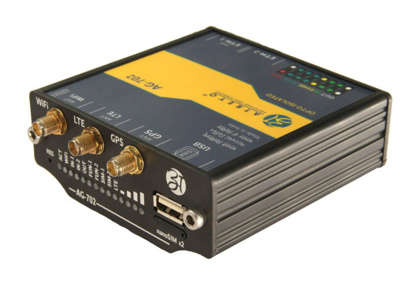
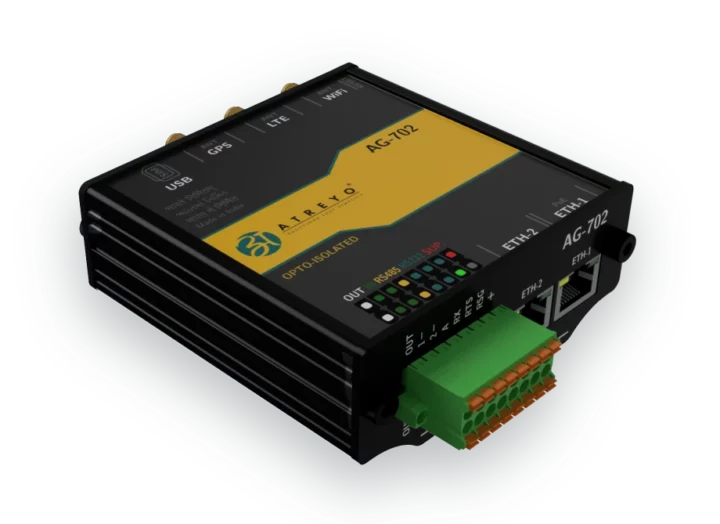
The Atreyo AG-702 is an industrial OpenWrt gateway powered by the MediaTek MT7628 processor, featuring dual Ethernet and WiFi connectivity alongside an integrated LTE and GNSS modem capable of accommodating two SIM cards.

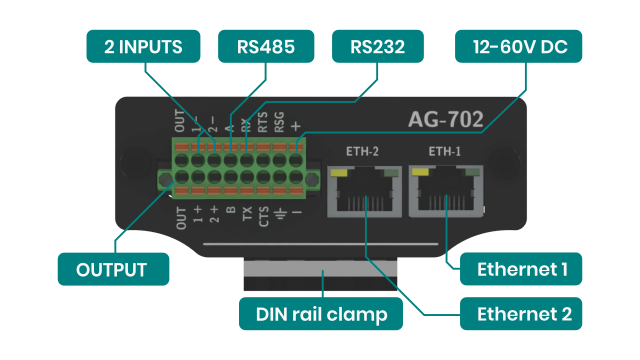
This gateway boasts isolated RS485 and RS232 interfaces for reliable communication, two digital isolated inputs, one relay output, and a USB host port that facilitates connections to peripherals like flash drives or USB converters, enhancing its versatility across different interfaces. Encased in an anodized aluminum enclosure, it offers robust durability suitable for industrial environments.

Furthermore, the Atreyo AG-702 supports a wide input voltage range of 14-60V DC, ensuring compatibility with various industrial power systems and enhancing its adaptability to diverse settings.

AG-702 Interfaces Rear Panel

Atreyo AG-702 specifications:

  1. SoC: MediaTek MT7628 MIPS processor at 580MHz
  2. System Memory: 256MB
  3. Storage:
    • 32MB eMMC flash
    • 512MB NAND flash with ExtRoot support (overlay)
  4. Networking:
    • 100Mbps Ethernet WAN port
    • 100Mbps Ethernet LAN port
    • LTE/GPRS with dual SIM and 1x external antenna
    • 2.4 GHz WiFi with 1x external antenna
    • GNSS with active antenna support
  5. USB: 1x USB 2.0 Type-A port
  6. Serial Interfaces:
    • Isolated RS485
    • Isolated RS232
  7. Expansion:
    • 2x isolated digital input
    • 1x relay output
  8. Miscellaneous:
    • LED indicators for system, I/Os, WiFi, SIM card, LTE, and signal strength
  9. Power Supply:
    • 14 to 60V DC via terminal block
    • Passive PoE support
  10. Dimensions: 88 x 87 x 35mm (Aluminium housing with DIN rail mounting option)
  11. Weight: 240 grams

The AG-702 is said to run OpenWrt 23.05 with the Atreyo Environment V1.01b and Linux kernel 5.15.71.

The default firmware installed on the Atreyo AG-702 industrial OpenWrt gateway offers a wide array of advanced features designed to enhance functionality and flexibility. Among these features is robust VPN support, including protocols such as OpenVPN and WireGuard, ensuring secure and encrypted communication over public networks. Additionally, the gateway supports the ModBus protocol, serving various roles like TCP slave, TCP master, RTU master, and RTU gateway, enabling seamless integration with ModBus-enabled devices in industrial environments.

RS485 dual Ethernet gateway

For remote management, the gateway provides multiple avenues such as a user-friendly Web UI for configuration and monitoring, SSH access for secure command-line interface management, SNMP for network device monitoring, and MQTT(s) for efficient communication in IoT applications. These capabilities empower administrators to efficiently manage and monitor the gateway and connected devices, making it well-suited for industrial deployments requiring secure, reliable, and scalable communication solutions. Atreyo also provides an SDK allowing users to develop their application(s) for the gateway. Additional information about the hardware and software can be found on the documentation website.

Atreyo told CNX Software the AG-702 industrial OpenWrt gateway is available now with pricing starting at $125 without cellular and GNSS connectivity. I can also see they have offices in India and Poland, so European companies should also be able to easily source the gateway. More details may be found on the product page.

Revolutionizing Wireless Connectivity: Exploring the Compex WLE7002E25 WiFi 7 Mini PCIe Module

The Compex WLE7002E25 is a WiFi 7 module designed in a standard mini PCIe form factor, ensuring compatibility with existing systems using WiFi 4 or WiFi 5 modules. This compatibility simplifies integration for device manufacturers, as they do not need to modify their hardware to accommodate the new generation WiFi 7 module. As a result, development costs are reduced, and time-to-market is accelerated.

One of the key achievements of the WLE7002E25 is its lower power consumption while maintaining impressive transmit power levels. Compared to the high-performance Qualcomm reference design, the WLE7002E25 module offers a 50% reduction in size and significantly lower power consumption with a minor loss in performance. The module boasts a maximum transmit power of 22dBm in the 2.4GHz band and 21dBm in the 5GHz band, with a maximum power consumption of 8.0W.

An important feature of WiFi 7 is Multi-Link Operation (MLO), allowing clients to connect to an Access Point (AP) through multiple bands simultaneously, reducing latency. The WLE7002E25 supports MLO between its 2.4GHz and 5GHz bands and implements MLO signals between adapters, enabling MLO with other WiFi 7 modules such as the Compex WLE7000E6. This MLO capability is crucial for applications requiring low latency, such as games, robotics, real-time translation, and teleconferencing.

The WLE7002E25 also offers open-source Ath12k driver support, ensuring seamless integration with non-Qualcomm platforms like x86 embedded boards. Despite its advanced features, the WLE7002E25 is competitively priced, making it an attractive option for migrating from WiFi 4 and WiFi 5 to WiFi 7 directly, bypassing WiFi 6 development costs. The Compex WLE7002E25 is not just a WiFi 7 mini PCIe module but an investment in the future of wireless connectivity, offering cutting-edge technology, comprehensive features, and diverse application potential.

The Compex WLE7002E25 represents more than just a WiFi 7 mini PCIe module; it’s an investment in the future. With its cutting-edge technology, comprehensive features, and diverse application potential, the Compex WLE7002E25 stands poised to rewrite the rules of wireless connectivity.

Exploring the Security and Performance Features of nRF9151: A Breakdown of Arm Cortex-M33, TrustZone, and CryptoCell

The newly developed System-in-Package (SIP) is a significant advancement for power-efficient cellular projects. It features a 64MHz Arm Cortex-M33 processor, LTE-M/NB-IoT cellular connectivity, and DECT NR+ connectivity, all integrated into a single chip. What sets this SIP apart is its remarkable one-fifth footprint reduction compared to previous solutions. This reduction in size makes it ideal for applications where space is limited but advanced cellular capabilities are required, offering a compact yet powerful solution for a range of IoT and mobile communication projects.

Nordic Semiconductor has announced a new addition to its nRF91 family, introducing the nRF9151 system-in-package (SiP). This innovative SiP integrates a system-on-chip (SoC), power management features, and a radio frequency front end (RFE) tailored for cellular connectivity. Notably, Nordic Semiconductor claims a substantial 20 percent reduction in footprint with the nRF9151, making it well-suited for wearables, sensors, and other compact projects.

A development kit will be offered when the part hits general availability, the company has confirmed

Kjetil Holstad from Nordic Semiconductor highlights that a deep understanding of market demands and customer challenges drove the development of the nRF9151. The goal of the nRF9151 is to streamline the development process, reduce power consumption, and minimize footprint. This strategic addition to Nordic’s cellular IoT portfolio emphasizes its commitment to providing advanced solutions and staying at the forefront of the industry.

The nRF9151 from Nordic Semiconductor is fully compatible with its existing nRF9161 and nRF9131 parts, including the same modem firmware. Compared to the nRF9161, it introduces Power Class 5 20dBm operation alongside Power Class 3 23dBM support, along with a 20 percent reduction in footprint. This makes it ideal for power- and space-constrained designs like wearables. Additionally, it supports 3GPP Release 14 LTE-M and NB-IoT connectivity, as well as DECT NR+, a new technology for non-cellular local wireless connections in the 1.9GHz spectrum, offering low-latency high-reliability connections and support for large mesh networks.

The nRF9151 includes a single 64MHz Arm Cortex-M33 microcontroller core, 256kB of static RAM (SRAM), and 1MB of onboard flash memory outside the radio hardware. This setup provides the necessary computational power and storage capacity for various applications.

In terms of security, the chip supports Arm’s TrustZone security technology which provides a hardware-based security foundation for system software, enabling secure execution environments and protecting sensitive data. Additionally, it features CryptoCell, an embedded security system that targets power-and-area-constrained designs. CryptoCell offers cryptographic acceleration to enhance the performance of encryption and decryption tasks and includes a true random number generator (TRNG) for generating cryptographic keys and ensuring secure communication channels.

The nRF9151 is sampling now, Nordic has confirmed, with no word yet on pricing or general availability. More information is available on the Nordic website.

Introducing WeAct STM32G4: Tiny Development Board with Versatile Microcontroller Options

The WeAct STM32G4 is a compact development board that utilizes the STMicro STM32G4 Arm Cortex-M4F mixed-signal microcontroller. This microcontroller operates at a clock speed of 170 MHz and comes equipped with DSP (Digital Signal Processing) instructions, making it suitable for a wide range of applications.

Key features of the WeAct STM32G4 board include:

  • Microcontroller: It is based on the STM32G4 microcontroller, which is known for its mixed-signal capabilities, making it ideal for applications such as motor control, building automation, lighting control, digital power meters, and more.
  • Compact Size: The board is designed to be tiny, making it convenient for prototyping and integration into space-constrained projects.
  • High Performance: With a clock speed of 170 MHz, the STM32G4 microcontroller delivers high processing power and efficiency for real-time applications.
  • Mixed-Signal Capabilities: The microcontroller’s mixed-signal architecture enables it to handle analog and digital signals simultaneously, making it versatile for a wide range of tasks.

The WeAct STM32G4 development board is available in two versions, each powered by a different STM32 microcontroller. The first version features an STM32G474CEU6 “Hi-resolution line” microcontroller with 128KB RAM and 512KB flash memory, making it suitable for applications requiring higher processing power and memory capacity. On the other hand, the second version is equipped with an STM32G431CBU6 “Access Line” MCU, offering 32KB RAM and 128KB flash memory, which is more suitable for basic applications with lower memory and processing requirements. Both versions of the board come with a USB-C port for power supply and programming, three buttons for user interaction or control, and two 24-pin headers for connecting peripherals and expansion modules. These features make the WeAct STM32G4 board versatile and adaptable to a wide range of projects, from simple applications to those demanding higher performance and memory capabilities.

WeAct STM32G4 schematics

The WeAct STM32G4 development board is available with two microcontroller options:

  • STMicro STM32G431CBU6: Arm Cortex-M4F MCU @ 170 MHz with DSP instructions, 32KB RAM, and 128KB flash.
  • STMicro STM32G474CEU6: Arm Cortex-M4F MCU @ 170 MHz with DSP instructions, 128KB RAM, and 512KB flash; includes a high-resolution timer and complex waveform builder plus event handler (HRTIM) for digital power conversion applications.

Additional features include:

  • 1x USB Type-C port for power and programming.
  • 2x 24-pin headers with GPIOs, ADC, DAC, I2C, USART, LPUART, OAmp, CAN Bus, timer outputs, etc.
  • 4-pin SWD header for debugging.
  • Compact size: 36.28 x 28.14 mm.
  • Power supply support from 3.3V to 20V DC via USB-C port.
  • MicrOne ME6216A33XG voltage regulator providing 3.3V output.

WeAct Studio does provide the PDF schematics, the STM32G4 datasheet, and TRM, some code samples (Blink, ADC, RTC, MSC, SPI flash), and the WeAct Studio Download Tool (Windows only) to flash the firmware via USB or UART. You’ll find those resources on GitHub for both the value line board and the hi-resolution line board, but most people will need to check the tools and documentation on the STMicro website as well.

The other benefit of those boards is their price, the board goes for $2.92 and $5.79 for the STM32G431CBU6 and STM32G474CEU6 models respectively, including GPIO and SWD headers, but not shipping which adds about $1 in my case. For reference, the official STMicro NUCLEO-G491RE board is sold for $15.

Questwise Ventures Introduces Energy-Harvesting Wireless Transmitter/Receiver for IoT Connectivity

Los Gatos-based Questwise Ventures has launched a new gadget which aims to deliver Internet of Things (IoT) connectivity without the need to power the transmitting side — by using an energy-harvesting push-button capable of driving its own radio.

Los Gatos-based Questwise Ventures has launched a new gadget that aims to deliver Internet of Things (IoT) connectivity without the need to power the transmitting side — by using an energy-harvesting push-button capable of driving its radio.

Questwise Ventures, based in Los Gatos, has introduced a groundbreaking gadget called the Energy-Harvesting Wireless Transmitter & Receiver. This device is designed to provide Internet of Things (IoT) connectivity without requiring a power source on the transmitting end. It achieves this by utilizing an energy-harvesting push-button that can power its radio transmission.

The key innovation lies in the specially designed button, which features an inventive spring mechanism. When the button is pressed, it efficiently captures and releases energy generated during the press. This energy is then directed to a coil, which in turn powers the transmitter, enabling seamless transmission of a single signal.

The Energy-Harvesting Wireless Transmitter & Receiver represents a revolutionary solution for IoT connectivity, allowing for energy-efficient and self-powered wireless communication.

Questwise Ventures‘ Energy-Harvesting Wireless Transmitter & Receiver builds upon a technology that has already seen use in self-powered door chimes. In this familiar scenario, the button outside the door draws the energy needed for transmission from the physical act of pressing the button, eliminating the need for a power source.

Similarly, Questwise’s device includes a transmitter that harnesses energy from the push-button mechanism. This transmitter is paired with a receiver designed for connection to a microcontroller or another powered device. When the transmitter sends a signal — which can be received from up to a couple of meters away — the receiver can then generate a momentary pulse or a latching toggle signal. This signal can be interpreted and acted upon according to the user’s needs or preferences.

The boards come as a matched pair, and can operate to a range of over six feet. (📷: Questwise Ventures)
The boards come as a matched pair, and can operate to a range of over six feet.

“Using a self-powered transmitter in situations where the receiver needs to be powered can offer distinct advantages, particularly in scenarios where you want to minimize maintenance, increase reliability, or enhance convenience,” the company says, suggesting it could find a use for everything from doorbells to emergency signaling.

The transmitter and receiver are available as a matched pair on the Questwise Ventures Tindie store, priced at $21.30.

Vodafone and Lime Microsystems Unveil Upgraded 5G Network-in-a-Box with Raspberry Pi 5 Integration

Cellular network giant Vodafone and software-defined radio specialist Lime Microsystems have announced they will be showing off a revamped version of their 5G network-in-a-box device, built around a Raspberry Pi 5 single-board computer.

Cellular network giant Vodafone and software-defined radio specialist Lime Microsystems have announced they will be showing off a revamped version of their 5G network-in-a-box device, built around a Raspberry Pi 5 single-board computer.

Vodafone and Lime Microsystems have collaborated to develop an advanced 5G network-in-a-box solution, which is based on a Raspberry Pi 5 single-board computer. This innovative device represents a significant upgrade over previous designs, offering higher bandwidth, a smaller physical size, and reduced power consumption.

The network-in-a-box device is designed to provide a complete 5G network solution in a compact and efficient package. It leverages software-defined radio (SDR) technology, allowing for flexible and customizable network configurations. This enables faster deployment of 5G networks in various environments, including remote areas, temporary setups, and specialized applications.

By utilizing the Raspberry Pi 5 as the core computing platform, the new network-in-a-box solution benefits from its powerful processing capabilities, versatile connectivity options, and widespread developer support. This makes it easier for developers and network operators to integrate and customize the device according to their specific needs and requirements. The collaboration between Vodafone and Lime Microsystems showcases the ongoing innovation and evolution in the field of 5G networks, providing a glimpse into the future of flexible, scalable, and efficient network solutions.

“Following on from the success of last year’s unveiling of the Raspberry Pi 5G network-in-a-box at Mobile World Congress, Vodafone is introducing a new improved version at MWC24 with numerous use cases, ranging from network coverage extension to 5G network delivery via drone,” says Lime Micro’s Andrew Back.

According to Lime Micro’s Andrew Back, the new system will be fully compatible with Raspberry Pi 5, providing improved compute performance for addressing various use cases, including network coverage extension and 5G network delivery via drones. The project is a continuation of the success seen with last year’s Raspberry Pi 5G network-in-a-box unveiled at Mobile World Congress.

The new system is based on LimeNET CrowdCell, an open radio access network (open RAN) solution that utilizes Lime Micro’s LimeSDR software-defined radio technology. It serves as a small cell network base station for rapid deployment and remote reconfiguration. The latest revision integrates the Raspberry Pi 5, offering enhanced computing capabilities over previous models.

The LimeNET CrowdCell (pictured) is getting a smaller, lower-power successor, powered by a Raspberry Pi 5.

Back mentions that the Lime radio module has undergone further improvements for lower power consumption and a smaller form factor. Optimized drivers for the efficient Amarisoft 5G software stack enable the deployment of a self-contained, plug-and-play network solution for various use cases.

The new model is set to launch in the first half of the year and will be demonstrated during Mobile World Congress (MWC)2024  at Vodafone’s booth in Hall 3, Stand 3E11.

PiEEG A Raspberry Pi Shield for Measuring Biosignals like ECG, EMG, and EEG, Available for Just $350

PiEEG: An 8-channel, open-source Raspberry Pi shield for easy EEG, EMG, and ECG measurement. User-friendly and electrode-compatible.

PiEEG is an 8-channel, open-source shield for Raspberry Pi, designed to easily measure EEG, EMG, and ECG biosignals. It’s user-friendly and compatible with various electrodes, making it easy to explore complex biosignals without needing specialized equipment.

Researchers at Heriot-Watt University have developed the PiEEG, a cost-effective and precise Raspberry Pi shield that turns the device into a brain-computer interface. This 8-channel tool enables real-time EEG signal measurement and processing, facilitating projects like thought-controlled robots, sleep and meditation monitoring, lie detection, and more. The PiEEG’s mission is to make neuroscience widely accessible, targeting educational uses in universities and schools with Raspberry Pi.

The PiEEG device uses a Texas Instruments ADS299 analog-to-digital converter for precise reading of brain signals in microvolts from the scalp, converting them to digital form for Raspberry Pi. Due to EEG data’s susceptibility to noise from electromagnetic interference, poor contact, and human movement, the device includes software with a bandpass filter to clean up the data in real-time. The software, written in C, C++, and Python allows for flexible data reading, processing, and display, making it adaptable for various projects.

Scheme of connecting electrodes to the PEEG plan: 1 – EEG electrode, 2 – reference electrode, 3 – ground electrode, 4 – bias electrode

PiEEG Raspberry Pi Shield Specifications:

  • Compatible with Raspberry Pi 3,4 or 5
  • 8 channels for connecting wet or dry electrodes
  • Data transfer via SPI protocol with a frequency from 250 SPS to 16 kSPS and a resolution of 24 bits per channel
  • Programmable signal gain: 1, 2, 4, 6, 8, 12, 24
  • Ability to measure impedance
  • LEDs for power indication and ADS1299 connection indication
  • 3 free pins for connecting external objects (ground and Raspberry Pi channel)
  • Easy programming with Python

The company offers comprehensive support for users, including a guide for making an electrode hat (manual) and various docs available on the GitHub repository.

For setup and usage, detailed documentation is provided, along with a video presentation and a demo). For academic references, see the IEEE publication (IEEE Xplore).

The device was Initially launched on Crowdsupply and is now available on Elecrow.

STMicroelectronics reveals advanced ultra-low-power STM32 microcontrollers

New flagship in ultra-low-power consumes less, delivers more at effective cost

STMicroelectronics has introduced a new generation of energy-conscious and cost-effective microcontrollers (MCUs) that can reduce energy consumption by up to 50% compared to previous product generations. This enables less frequent battery replacements, minimizes the impact of discarded batteries, and allows more designs to go battery free running solely from an energy-harvesting system such as a small photovoltaic cell.

In the global pursuit of sustainability, technologies deployed in smart buildings and Internet of Things (IoT) applications are critical tools for managing energy and resources efficiently. At the heart of the smart sensors and actuators making them possible, ST’s microcontrollers manage the processes that collect, filter, analyze, and act, communicating with high-level applications in the cloud. There are billions of these MCUs in action already and the expansion of smart living and working will demand billions more.

“It’s vital that these pervasive devices consume as little energy as possible as they help to minimize waste elsewhere. The new STM32U0 microcontroller series we are introducing today takes this notion to a new level, building on our proven ultra-low-power technologies,” explained Patrick Aidoune, General Purpose MCU Division General Manager, STMicroelectronics. “In fact, our new MCUs consume so little power that small devices in some dedicated applications like industrial sensor management can run for twice as long from the same size battery. This comes with the opportunity to add more advanced features and deliver cost-effective solutions for a variety of industrial, medical and consumer devices.”

The new STM32U0 MCUs enable this great leap in energy efficiency through a combination of their state-of-the-art design techniques and advanced manufacturing process. These include extremely low static power consumption in standby mode and superior wake-up performance, enabling the MCU to spend more time in power-saving sleep modes to minimize average energy demand.

One lead customer, in the security-systems market, is using the STM32U0 in security cameras to wake the device when motion is detected and thus enhance surveillance while saving energy. Another has created ultra-long-lasting smoke detectors, while a further application, by Ascoel, is using the STM32U0 to manage power-conscious functions of a water meter.

“Ascoel builds a wide range of innovative electronic devices with a focus on IoT technologies. We are working to design an ultrasonic water meter, with battery lasting for more than 10 years, integrating an LCD screen for real-time data, as well as the necessary security,” said Francesco Cerretani, Senior Software Developer, Ascoel. “We found that the STM32U0 was the perfect solution, supporting our goal to create a low-cost, ultra-low-power, easy-to-install, zero maintenance, precise water meter. When deployed at scale in the customer’s grid, it will improve control over water leakage and contribute to reducing the environmental impact.”

The STM32U0 enhances cost-effectiveness by providing an LCD segment display controller. Devices with an LCD, like Ascoel’s water meter as well as thermostats, smart retail labels, access-control panels, and factory automation can take advantage of this to reduce the cost of their PCB. Additional value-added features of STM32U0 MCUs include numerous analog peripherals like analog-to-digital converters (ADC), digital-to-analog converters (DAC), operational amplifiers, and comparators. There is also an on-chip system oscillator that helps cut the bill of materials to save costs and PCB space.

STM32U0 devices are the first MCUs running on Arm® Cortex®-M0+ targeting SESIP Level 3 and PSA level 1 focusing on firmware code protection. Certification provides an independent assurance of the STM32U0 security capabilities that product manufacturers can leverage to comply with the coming voluntary US Cyber Trust Mark and mandatory EU Radio Equipment Directive (RED).

Developers can also take advantage of up to 256KB of Flash, package options up to 81 pins, and 56MHz core speed, which are generous specifications for this class of device.

The STM32U0 series is in production now and ST is making the new devices available at an attractive price point starting at $0.68 for 1,000 units. Sample requests and further pricing options are available from local ST sales offices.

STMicroelectronics breaks the 20nm barrier for cost-competitive next-generation microcontrollers

Highlights

  • First STM32 microcontroller based on new technology to sample to selected customers in the second half of 2024.
  • 18nm FD-SOI with embedded phase change memory (ePCM) to deliver a leap in performance and power consumption.

STMicroelectronics announces an advanced process based on 18nm Fully Depleted Silicon On Insulator (FD-SOI) technology with embedded phase change memory (ePCM) to support next-generation embedded processing devices. This new process technology, co-developed by ST and Samsung Foundry, delivers a leap in performance and power consumption for embedded processing applications while allowing larger memory sizes and higher levels of integration of analog and digital peripherals. The first next-generation STM32 microcontroller based on the new technology will start sampling to selected customers in the second half of 2024, with production planned for the second half of 2025.

Remi El-Ouazzane, President of Microcontrollers, Digital ICs and RF products Group at STMicroelectronics, said:

As a leading innovator in the semiconductor industry, ST has pioneered and brought to our customers FD-SOI and PCM technologies for automotive and aerospace applications. We are now taking the next step to bring the benefits of these technologies to developers of industrial applications starting with our next-generation STM32 microcontrollers.”

Technology benefits

Compared to ST 40nm embedded non-volatile memory (eNVM) technology used today, 18nm FD-SOI with ePCM vastly improves key figures of merit:

  • More than 50% better performance-to-power ratio
  • 2.5-times higher non-volatile memory (NVM) density enabling larger on-chip memories
  • Three times higher digital density for integration of digital peripherals such as AI and graphics accelerators and state-of-the-art security and safety features
  • 3dB improvement in noise figure for enhanced RF performance in wireless MCUs

The technology is capable of 3V operation to supply analog features such as power management, reset systems, clock sources and digital/analog converters. It is the only sub-20 nm technology supporting this capability.

The technology also delivers the reliability required for demanding industrial applications thanks to robust high-temperature operation, radiation hardening, and data retention capabilities already proven in automotive applications.

Additional information on FD-SOI and PCM is available on ST.com

u-blox launches new GNSS platform for enhanced positioning accuracy in urban environments

The u-blox F10 platform increases positioning accuracy by reducing multipath effects, simplifying the process of promptly locating a vehicle.

u-blox, a global provider of leading positioning and wireless communication technologies and services, has announced F10, the company’s first dual-band GNSS (Global Navigation Satellite Systems) platform combining L1 and L5 bands to offer enhanced multipath resistance and meter-level positioning accuracy. The platform caters to urban mobility applications, such as aftermarket telematics and micromobility.

Applications that use GNSS receivers for accurate positioning are on the rise. Yet, current receivers do not fully perform in urban areas. Accurate and reliable positioning in dense urban environments, where buildings or tree foliage can reflect satellite signals, requires GNSS receivers to mitigate multipath effects. The L5 band‘s resilience to these effects significantly improves positioning accuracy. Combined with the well-established L1 band, an L1/L5 dual-band GNSS receiver can deliver < 2 m positioning accuracy (CEP50), against about 4 m with the L1 band only. The u-blox team has conducted driving tests in several urban areas, confirming a significant improvement over GNSS L1 receivers.

The F10’s firmware algorithm prioritizes L5 band signals in weak signal environments, ensuring reliable positioning accuracy even when paired with small antennas. The platform is also equipped with protection-level technology that provides a real-time trustworthy positioning accuracy estimate.

When a cellular modem is extremely close to a GNSS receiver, it can interfere with the receiver’s reception. Some F10 module models (NEO-F10N, MAX-F10S, and MIA-F10Q) are equipped with a robust RF circuit that allows the GNSS and the cellular modem to operate without interference.

Video

The u-blox F10 platform is pin-to-pin compatible with the previous u-blox M10 generation for easy migration. It also supports u-blox AssistNow, which offers real-time online A-GNSS service with global availability to reduce GNSS time-to-first-fix and power consumption.

The u-blox EVK-F101 evaluation kit will be available in April 2024.

TOP PCB Companies