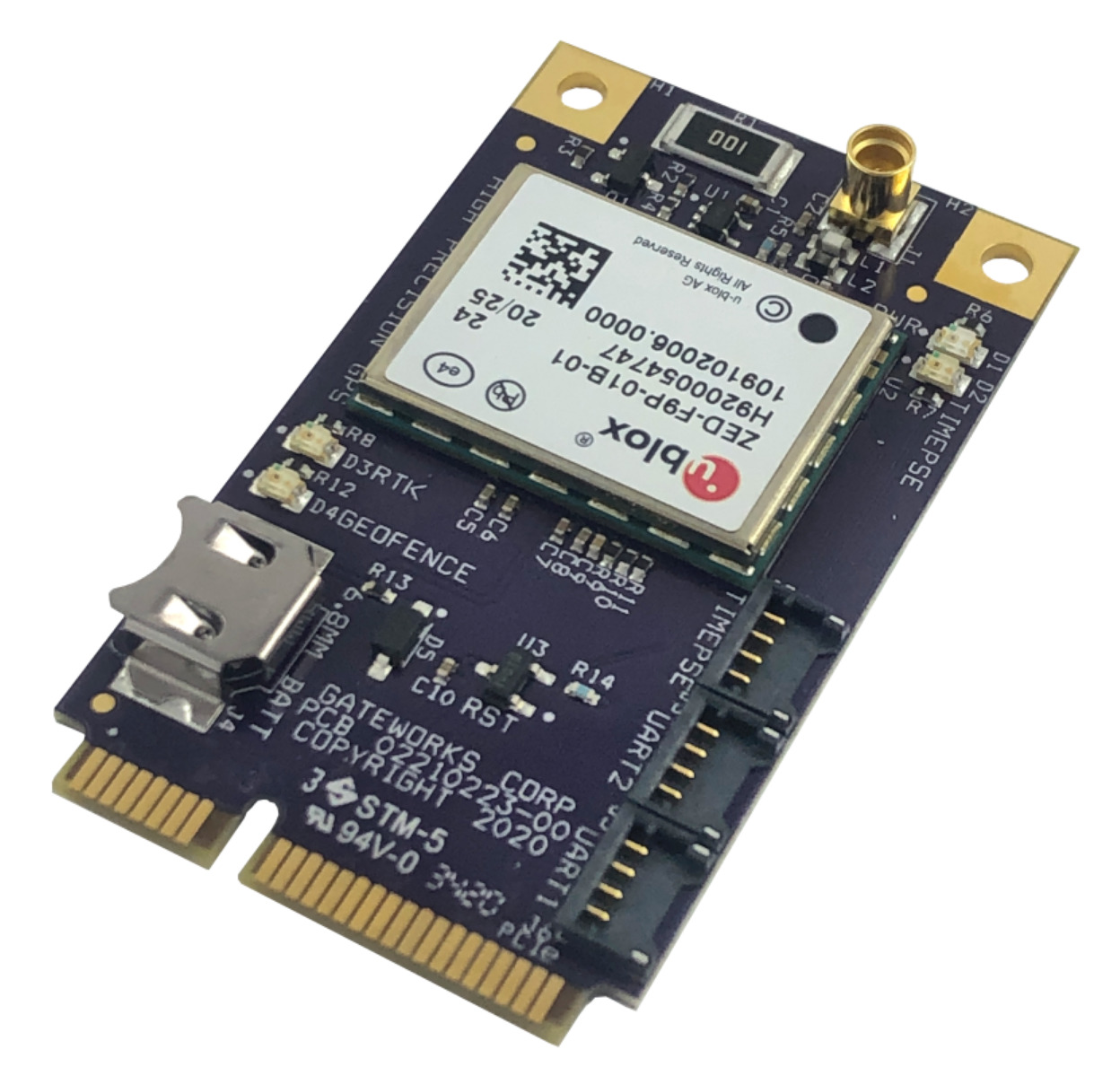
Gateworks is pleased to release a new high precision GNSS / GPS Mini-PCIe adapter based upon the u-blox ZED-F9P. The GW16143 enables precision navigation and automation of moving machinery in industrial applications such as agriculture, mining, and field mapping. Differential GNSS devices such as the GW16143 are starting to replace survey-grade equipment where precision is important. Multi-band Real-time kinematic (RTK) technology provides fast convergence times and reliable performance. The module supports both base and rover operation for RTK applications. Other radio cards such as the Gateworks GW16130 Iridium Satellite Modem or GW16132 CAT-M1 modem can provide communication links for the augmentation data.
GW16143 High Precision Mini-PCIe Card Highlights:
High Precision u-blox ZED-F9P GNSS/GPS Mini-PCIe Adapter
Concurrent reception of GPS, GLONASS, Galileo and BeiDou
Centimeter-level (<2cm) Accuracy GNSS positioning
Integrated Multi-Band Real Time Kinematics (RTK)
High update rate for highly dynamic applications
Allows for RTK “Base” and “Rover” Operation
Two UART headers for correction data over serial, PPS timepulse output header
Uses Standard NMEA, UBX and RTCM Message Format
Uses Mini-PCIe USB Signaling
Status LEDs
Rechargeable Lithium battery, 3.3V, 3mAH, 6.8mm
RTCM 3.x, SSR, SBAS Corrections
<1.0m SBAS, <0.2m SSR, <0.03m RTCM 3.x
Supports L1 and L2/L5 Bands
Rugged & Industrial design
-40C to +85C Industrial Operating Temperature
Made in the USA
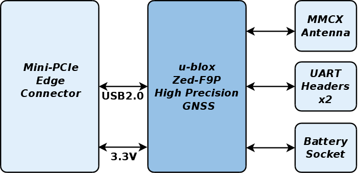
A MMCX antenna port allows for an external antenna. USB signaling is used on the Mini-PCIe connector to communicate with the host processor. Two UART headers are available to allow for correction data over serial. A PPS timepulse output header is also available. For faster cold start acquisition times, a rechargeable 3.3V lithium battery is provided.
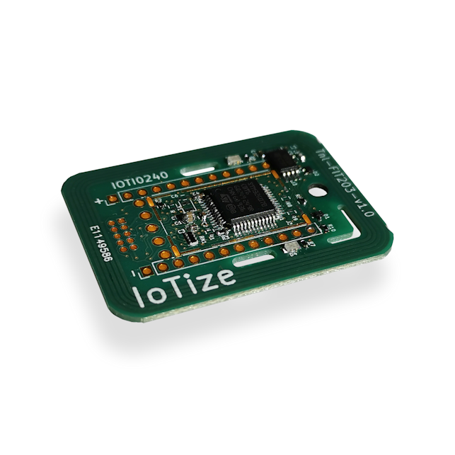
IoTize’s NFC module allows designers to add NFC 3-stroke configuration rapidly and with virtually no expertise
IoTize’s TapNLink TnL-FIT203 enhances user experiences with NFC 3-stroke configuration, providing an easy and secure way of viewing and updating appliance parameters using iOS or Android mobile phones. With NFC 3-Stroke configuration, users update parameters of appliances or machines in three steps:
approach the phone to the appliance to connect and read the actual configuration
view and modify settings in the mobile app
approach the phone to the appliance again to send the new parameters
With NFC, connecting mobile phones to appliances is automatic, intuitive, and secure. There are no addresses or codes to enter; just place the phone within a couple of inches of the NFC indicator on the appliance. The connection is established, data is read, and the appropriate app is launched instantaneously. Appliance users view and modify settings more easily with their mobile phones than with an on-board LCD-based user interface. Settings can even be stored and recalled for later use.
With TapNLink TnL-FIT203 appliance and equipment designers can add NFC 3-stroke configuration rapidly and with virtually no expertise. Designers simply connect TapNLink to their electronic design and configure it. The free IoTize Studio configuration software does the rest and automatically generates apps for iOS and Android mobile phones. No coding is required.
Features
Near field communication (NFC) Type5 tag (ISO/IEC 15693)
Configurable access profiles
Configurable, encrypted passwords
AES-128 data encryption
Configuration of up to 500 accessible data addresses
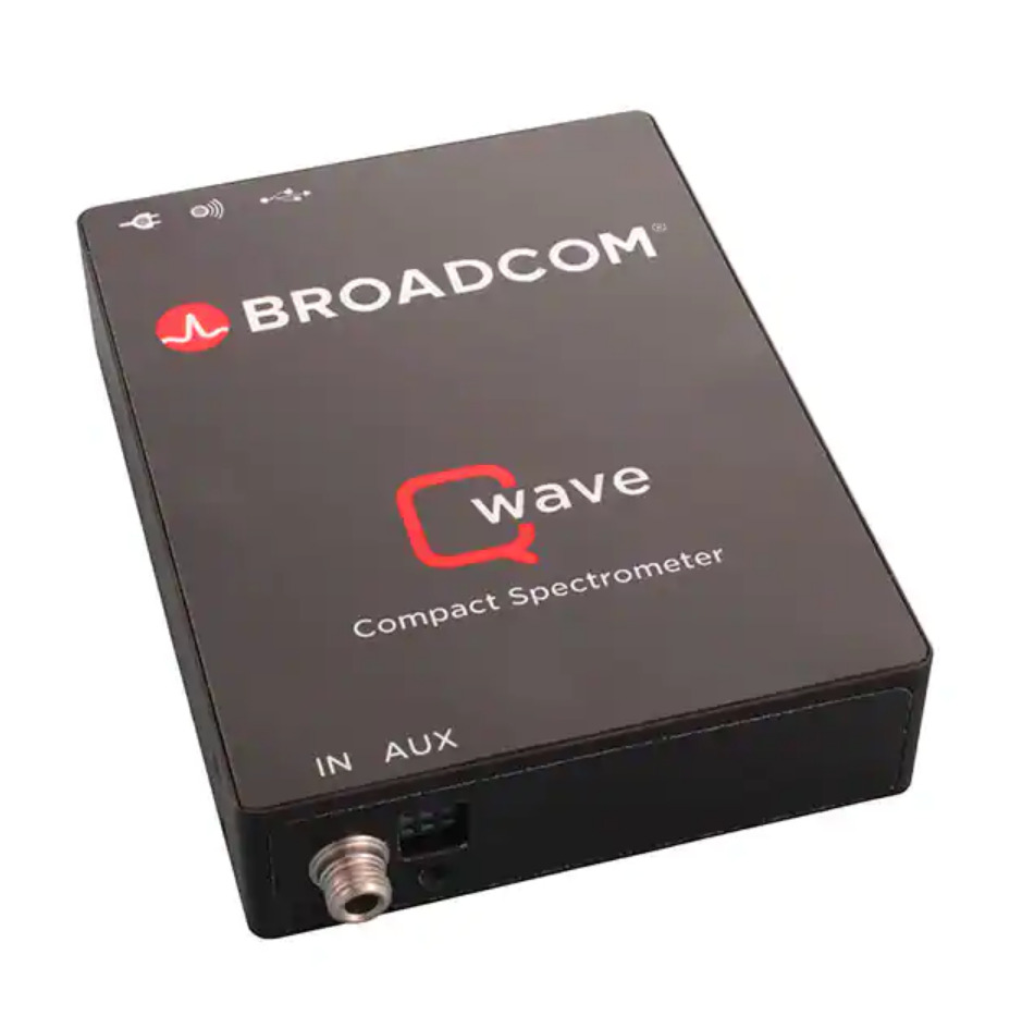
Qwave NIR–Compact USB spectrometer with high resolution and sensitivity for NIR measurements from 700 to 1030 nm
Armed with a high-resolution 3,648-pixel linear CCD detector, Broadcom’s Qwave 2 series can cope with bulkier spectrometer designs while maintaining a package size of 89.5 mm x 68.0 mm x 19.5 mm. Together with the smart spectrometer software Waves and various communication interfaces, the Qwave is the ideal spectroscopic instrument to be integrated into high-performance applications.
The TSZ181, TSZ182 are single and dual operational amplifiers featuring very low offset voltages with virtually zero drift versus temperature changes.
The TSZ181, TSZ182 are single and dual operational amplifiers featuring very low offset voltages with virtually zero drift versus temperature changes. They offer rail-to-rail input and output, excellent speed/power consumption ratio, and 3 MHz gain-bandwidth product, while consuming just 1 mA at 5 V. The device also features an ultra-low input bias current. These features make the TSZ18x ideal for high-accuracy high-bandwidth sensor interfaces.
Key features
Very high accuracy and stability
Rail-to-rail input and output
Low supply voltage: from 2.2 to 5 V
Low power consumption: 1 mA max. at 5 V
Additional features
Very high accuracy and stability:
Offset voltage 25 µV max. at 25 °C, 35 µV over the full temperature range (-40 to 125 °C)
Rail-to-rail input and output
Low supply voltage: 2.2 – 5.5 V
Low power consumption: 1 mA max. at 5 V
Gain bandwidth product: 3 MHz
Automotive qualification
Extended temperature range: -40 to 125 °C
Micro packages: DFN-8 2 x 2, SO-8 and MiniSO-8
Additional Benefits:
Higher accuracy without calibration
Accuracy virtually unaffected by temperature change
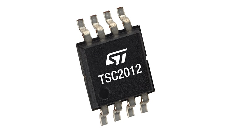
The TSC2010, TSC2011, and TSC2012 are precision bidirectional current sense amplifiers.
The TSC2010, TSC2011, and TSC2012 are precision bidirectional current sense amplifiers. They can sense the current thanks to a shunt resistor over a wide range of common-mode voltages, from -20 to +70 V, whatever the supply voltage is. They are available with an amplifier gain of 20 V/V for TSC2010, 60 V/V for TSC2011, and 100 V/V for TSC2012.
They are able to sense very low drop voltages as low as 10 mV full scale minimizing the measurement error.
The TSC2010, TSC2011, and TSC2012 can also be used in other functions such as: precision current measurement, overcurrent protection, current monitoring, and feedback loops.
Key features
Wide common-mode voltage: -20 to 70 V
Offset voltage: ±200 µV max
2.7 to 5.5 V supply voltage
Different gain options available – TSC2010: 20 V/V – TSC2011: 60 V/V – TSC2012: 100 V/V
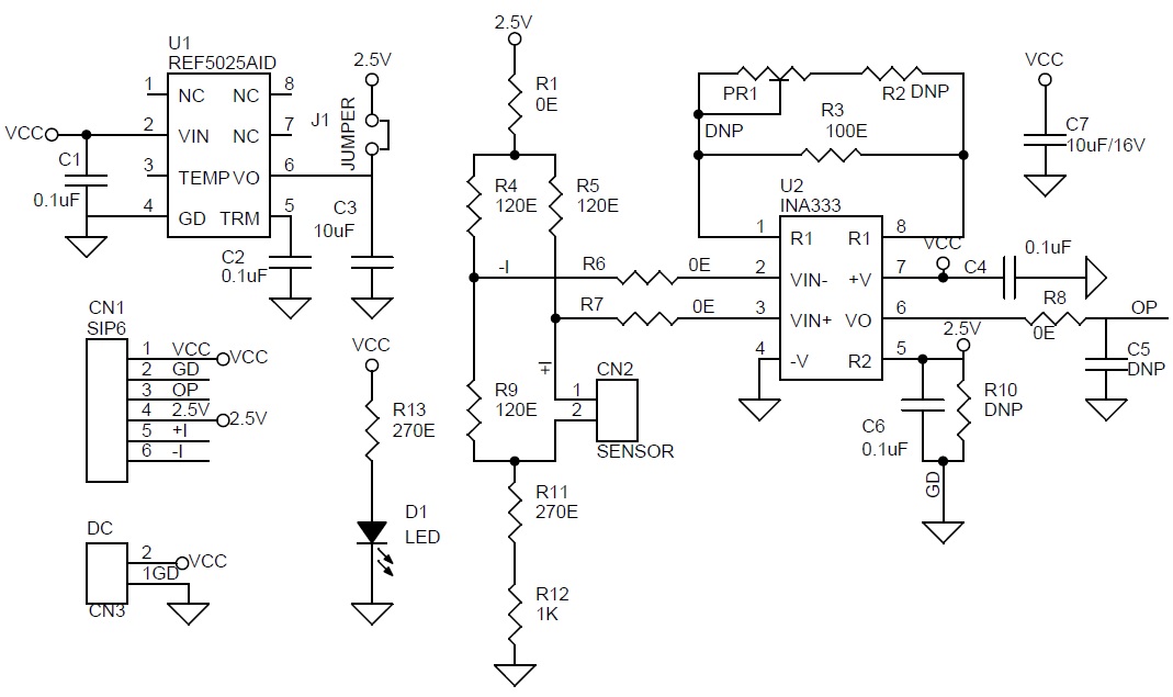
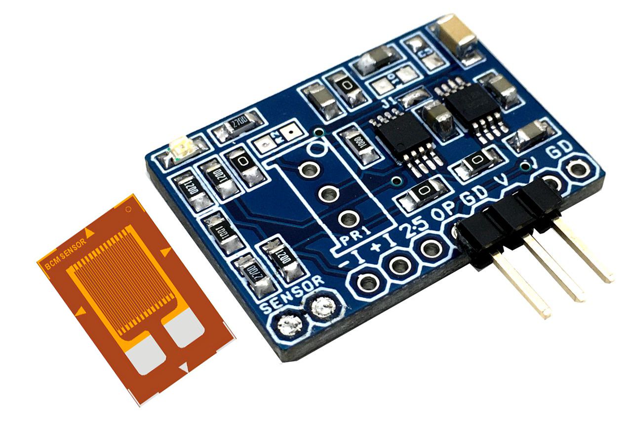
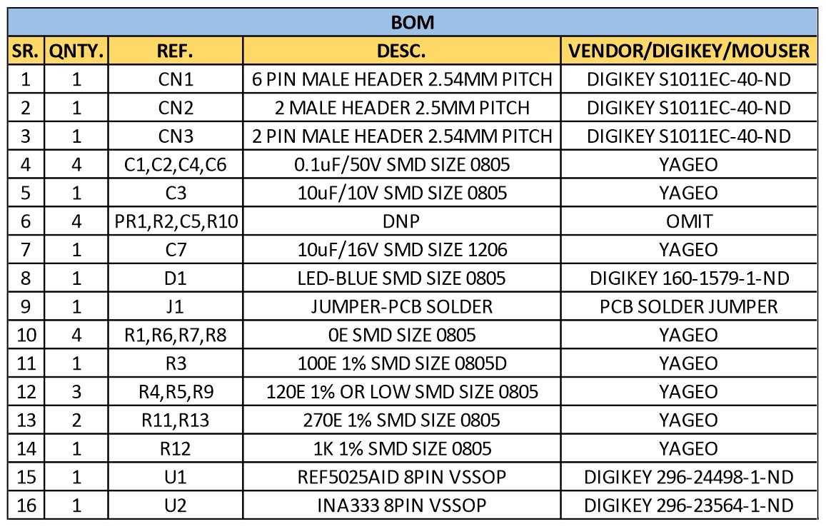
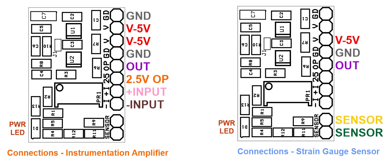
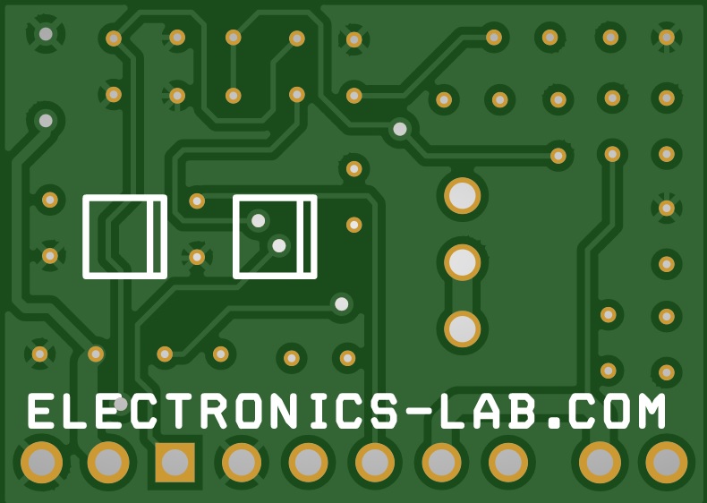
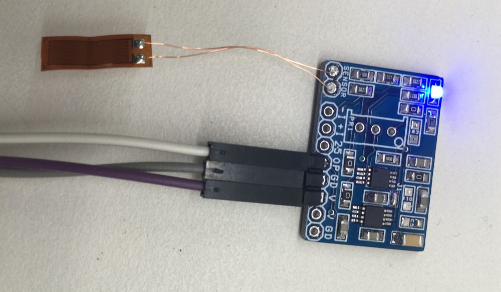
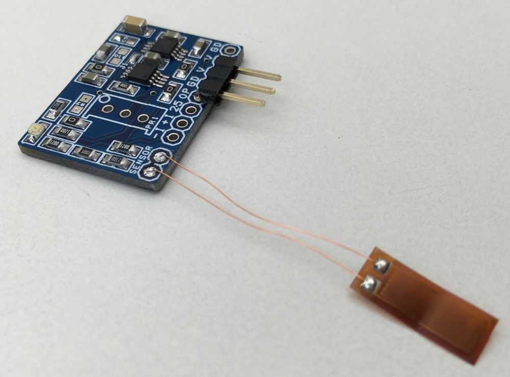
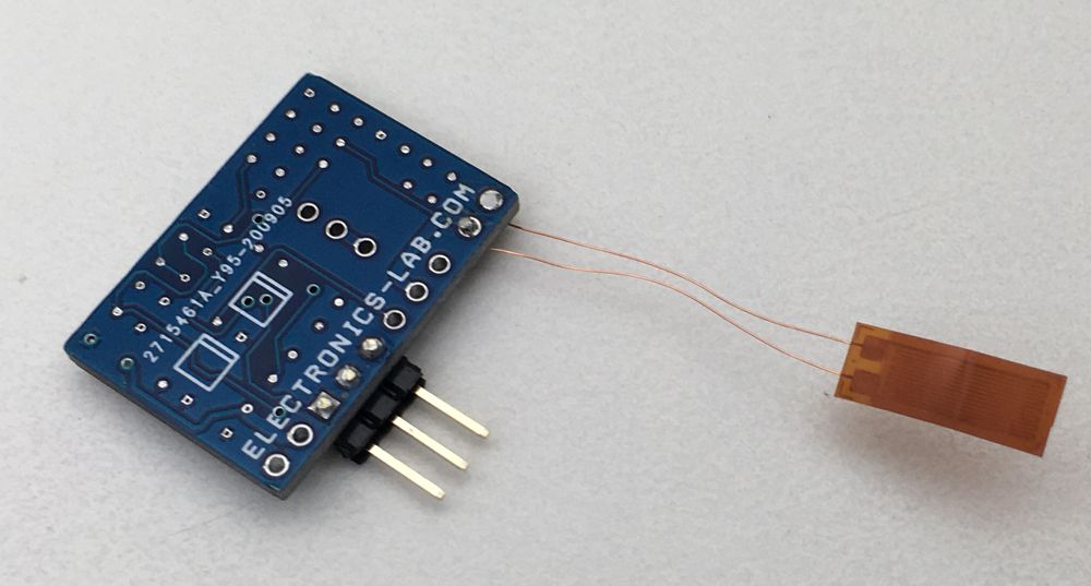
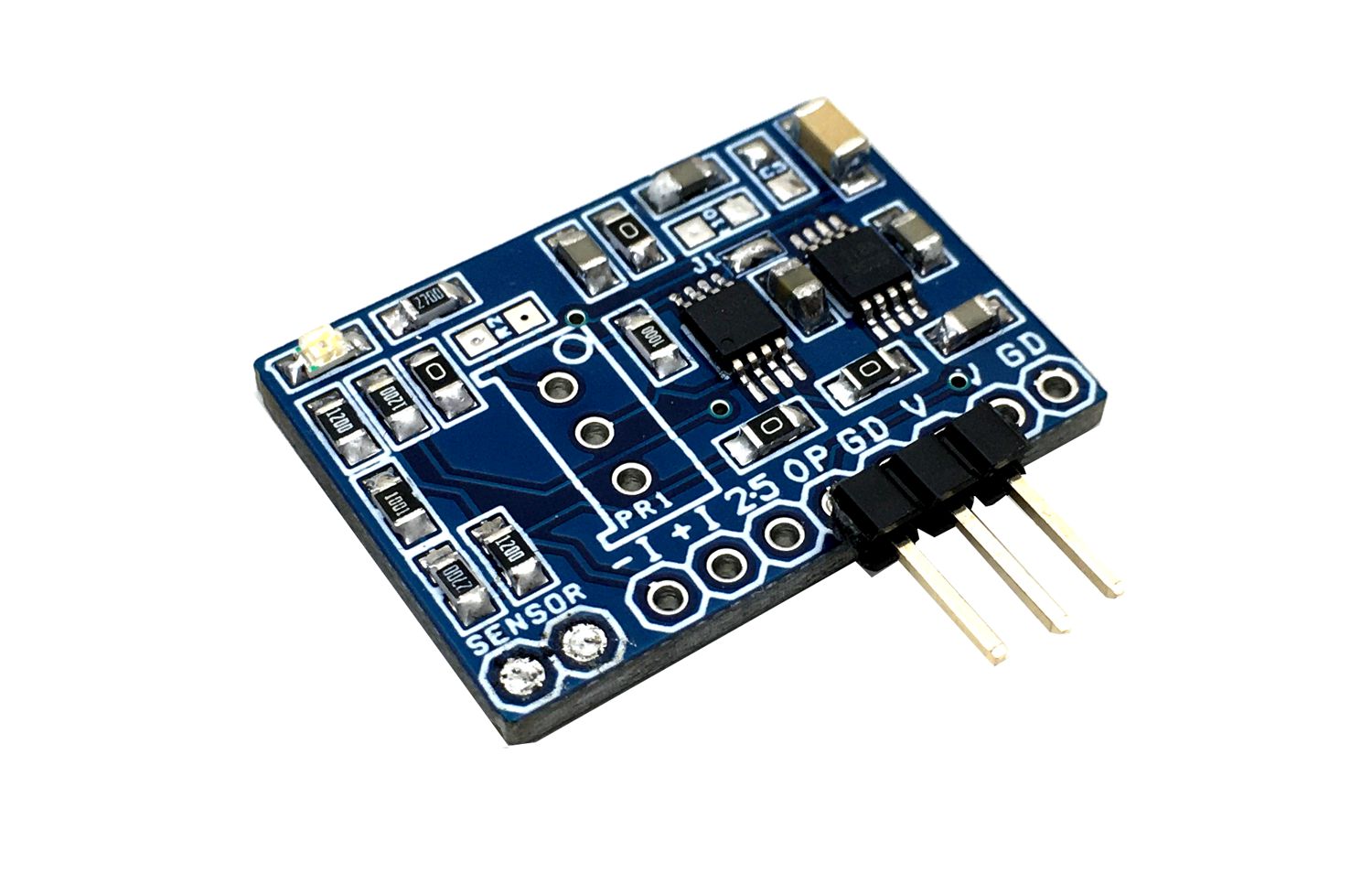
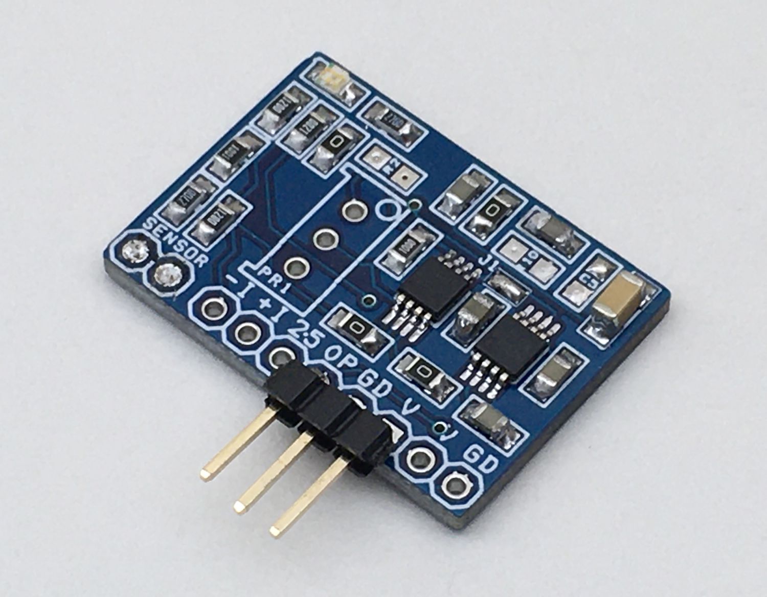
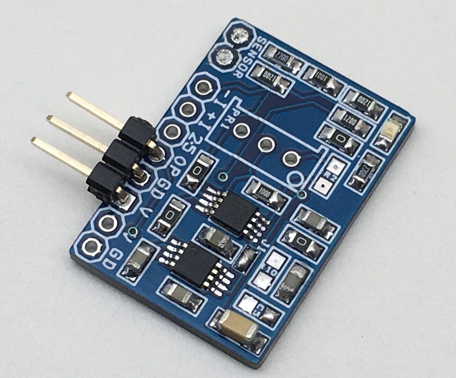
This is a new project, a single supply instrumentation amplifier with onboard bridge configuration, and a 2.5V precision reference voltage chip. The project can be configured for applications such as thermocouple amplifier, bridge amplifier, ECG amplifier, pressure sensors, medical instrumentation, portable instrumentation, RTD sensor amplifier. The project is based on INA333 micropower, zero drift, rail to rail out instrumentation amplifier chip. REF5025AID chip provides a precise 2.5V reference voltage. The board can be configured as an instrumentation amplifier or as a strain gauge amplifier with few easy changes.
We have tested this board as Strain Gauge Amplifier, circuit, Bom, Connection diagram, and information presented below.
Strain Gauge Amplifier
The circuit shown here is a simple example of a Strain Gauge Amplifier in a bridge configuration, this strain gauge circuit accurately measures the resistance of a strain gauge sensor placed in a bridge configuration. The resistance of the strain gauge sensor varies with applied force, change in resistance is directly proportional to how much strain the sensor is experiencing due to the force applied. Changes in the strain gauge resistance create a differential voltage that is amplified by an instrumentation amplifier INA333. The amplifiers have very high input impedance and therefore introduce negligible error with respect to the bridge resistance. The output voltage of the instrumentation amplifier will be depending on the sensor’s value and variation in resistance value. The bridge excitation voltage and instrumentation amplifier reference voltage 2.5V are supplied using the REF5025. A reference voltage at mid-supply (5V DC) biases the output voltage of the instrumentation amplifier to allow differential measurements in the positive and negative direction. The common mode resistors, R1, R11 and R12, have two main functions; limit the current through the bridge and set the common mode of the instrumentation amplifier. I have used 120 Ohms Strain Gauge sensor and thus I have chosen bridge resistors R4, R5, and R9 also 120 Ohms to match the sensors impedance. Matching the bridge resistors with the strain gauge resistance produces a 0 V differential bridge voltage when the strain gauge resistance is at its nominal value. It is advisable to use very low tolerance resistors to minimize the offset and gain error due to the bridge resistors. Operating power supply 5V DC, D1 power LED, J1 PCB jumper closed. CN2 sensor connection, CN1 supply input, and sensor output, R3 100 Ohms resistor set the gain of Amplifier to approx. 1001.
Note: I have used 120 Ohms strain gauge sensor, but different resistance sensor can be used, few available sensors are 350 Ω, 1000 Ω, and 3000 Ω. If a different nominal resistance is used, the bridge resistors must be chosen to match the nominal resistance of the strain gauge. The output voltage of the circuit will depend on the Gauge Factor of the Sensor.
Features
Power Supply 5V DC
Output 230mV to 4.7V DC
Strain Gauge Nominal Resistance 120 Ohms
Stain Gauge Resistance Variation 115 Ohms to 125 Ohms
Sensor Gauge Factor 5%
Bridge Excitation Voltage and Reference Voltage 2.5V DC
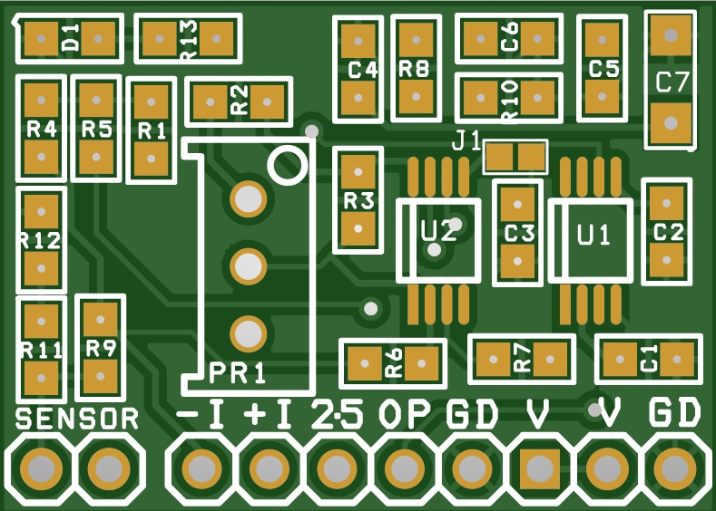
PCB Dimensions 26.99 x 19.21 mm
Strain Gauge Sensor
Digi-Key Part Number: MMF002504-ND
Manufacturer: Micro-Measurements (Division of Vishay Precision Group)
Manufacturer Part Number: MMF002504
Description: EA-06-250BG-120/LE STRAIN GAGES
Detailed Description: Linear Strain Gauge ±5% 0.250″ (6.35mm) 0.125″ (3.18mm)
Pattern Type: Linear
Strain Range: ±5%
Resistance: 120 Ohms
Resistance Tolerance: ±0.15%
What is a Strain Gauge Sensor?
A strain gauge is a sensor whose resistance varies with applied force. The change in resistance is directly proportional to how much strain the sensor is experiencing due to the force applied. Strain Gauge sensors are available in different types, configuration and different dimensions and resistance.
Resistance of Sensor
The electric resistance between the two metal leads, solder tabs or cable ends for connecting the measuring cable is called the resistance of a strain gauge. Strain gauges are available with 120-ohm, 350-ohm, 700-ohm 1,000 ohm or 3000-ohm resistance.
Gauge Factor of Sensor
The gauge factor k of a strain gauge is the proportionality factor between the relative change in resistance DR/R0 and the strain to be measured e: DR/R0 = k · e the gauge factor, a dimensionless number, is sometimes also called the k factor. This gauge factor is determined for each production batch by measuring and is specified on each strain gauge package as a nominal value complete with tolerance. The gauge factors vary between production batches by just a few thousandths.
The project also can be configured as a differential instrumentation amplifier for various applications. All-important pins of INA333 are easily accessible using header connectors to other devices or sensors. Omit R1, R4, R5, R9, R11, R12, Choose R3 or R2, and PR1 to adjust the gain of the amplifier, Choose R6, R7, 0ohms resistors, and differential pins +I and -I are available as input. Open the J1 jumper if the reference voltage is not required.
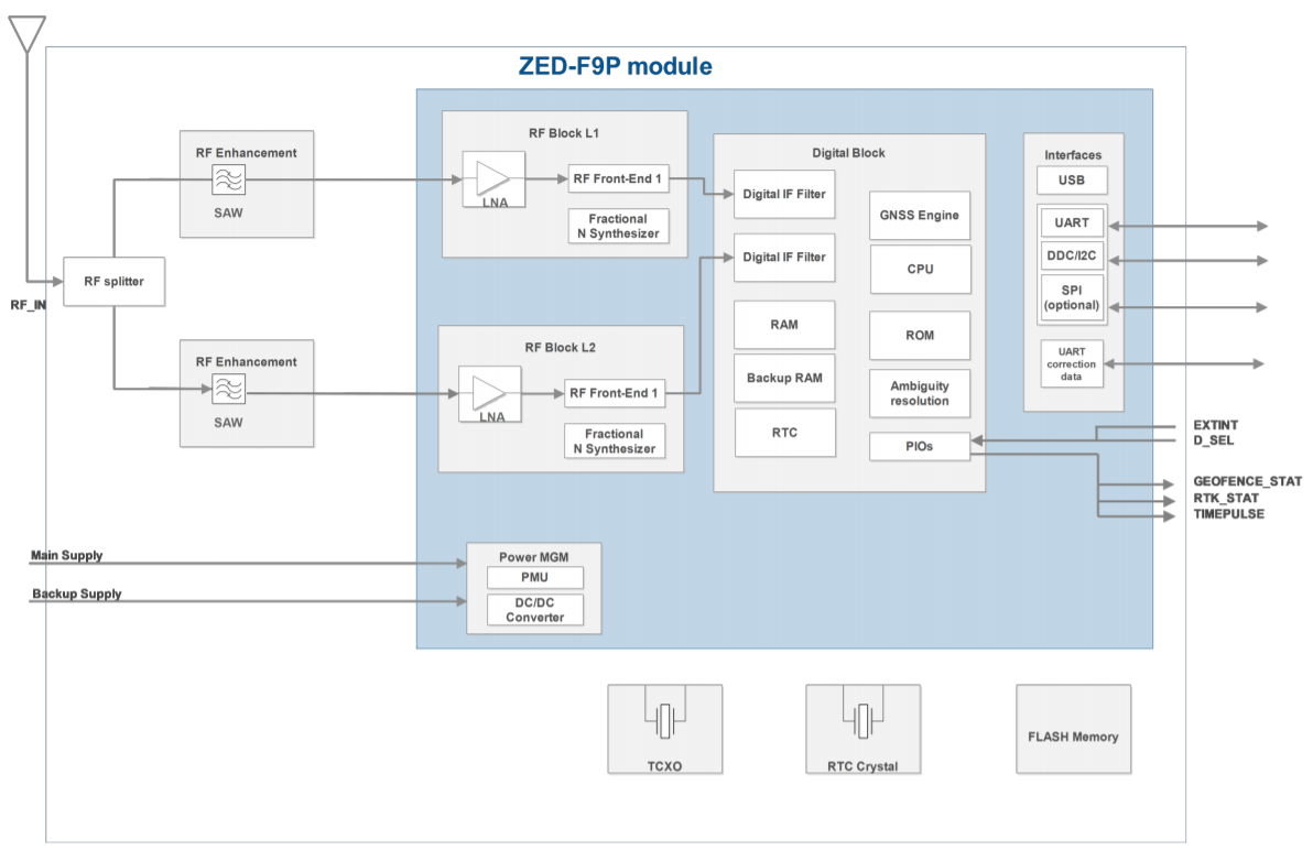
A little while ago, we covered a positioning receiver IC that enhanced positioning accuracy to centimeters due mostly to its cutting-edge capability of concurrent reception of multiple constellation data (GPS, GLONASS, BeiDou, and QZSSl, to be precise). Its name is the Teseo-LIV3F, from ST Microelectronics, and you can check the article link below, which I recommend if you are on the market for an above-average positioning module. Today, we will take a look at the new ZED-09P precision GNSS module, from U-Blox, that has some similarities, including, most notably, pinpoint accuracy.
So, let us take a step back. The ZED-09P from U-Blox is a precision GNSS module, featuring the F9 receiver platform from the same manufacturer, that provides multi-band RTK (Real-Time Kinematic) technology for industrial applications with centimeter-level accuracy, in a small form factor. The module allows for precise navigation and automation of moving machinery and also consumer-grade products. Another very important feature is moving base support, which allows for the base and rover to move while calculating their positioning accurately, making this a great candidate for UAV applications where the UAV has to follow a target or go to a moving platform and in cases where the relative position between both of them is relevant.
Just like the Teseo-LIV3F, it can receive and track multiple GNSS constellations, including the four major (GPS, GLONASS, Galileo and BeiDou), plus SBAS and QZSS satellites. All of them can be processed to provide an RTK navigation solution when used with correction data. Lastly, you can configure just a small subset of them, if power consumption is a concern in your project. Of course, before jumping right in you should take a look at the very well-documented integration manual, where the major concerns you should have in the design stage are set.
Block diagram of the U-Blox ZED-09P precision GNSS module
By diving deeper into it, you can see that a project with it takes a lot into consideration, and the features you get to come at the cost of a longer design stage, but on the other hand, the accuracy is insane. When you compare it with the Teseo-LIV3F, this module clearly brings more to the table, and it’s well expressed on its pricing, $199. You can also get an evaluation kit for $249. It clearly is tailored for professional-grade projects and can perform more expert tasks than the former. But is it worth the price tag, when you have a module built upon the same principle for a fraction of the price? I will leave that for your thoughts.
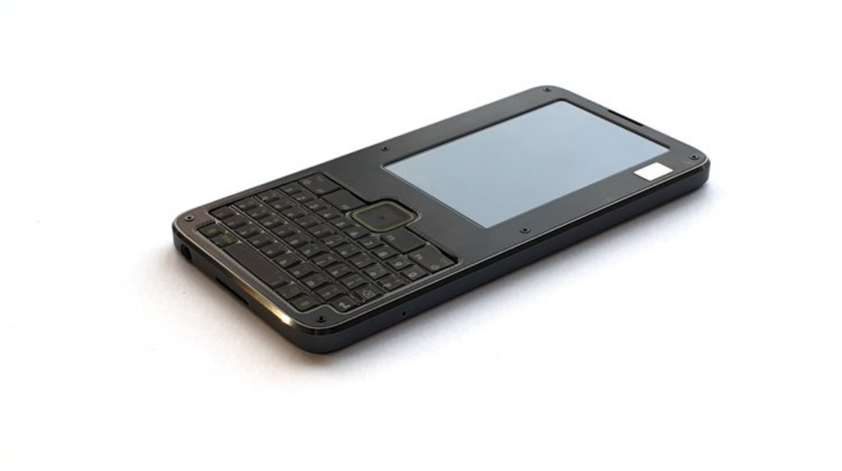
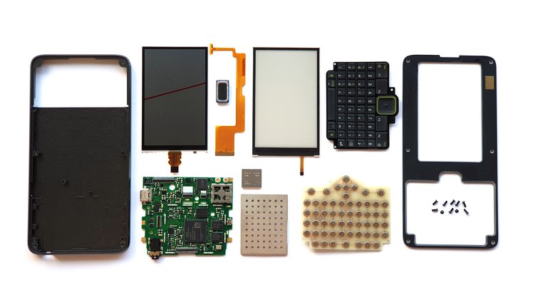
Precursor is a compact device with a physical keyboard, a built-in display, and an internal battery. It is an open hardware development platform for secure, mobile computation and communication, this device offers a system that users can have nearly complete control over, also with an added advantage of being smaller and lighter than an average smartphone. It has an FPGA that enables users to configure the chip so that it emulates several different processor types, giving users much more hardware power than a standard mobile device, The Precursor’s hardware is designed to be entirely inspectable and understandable by a single knowledgeable user, it is well suited as a hardware development framework for security-critical applications such as crypto wallets, secure messaging platforms, password managers and authenticators.
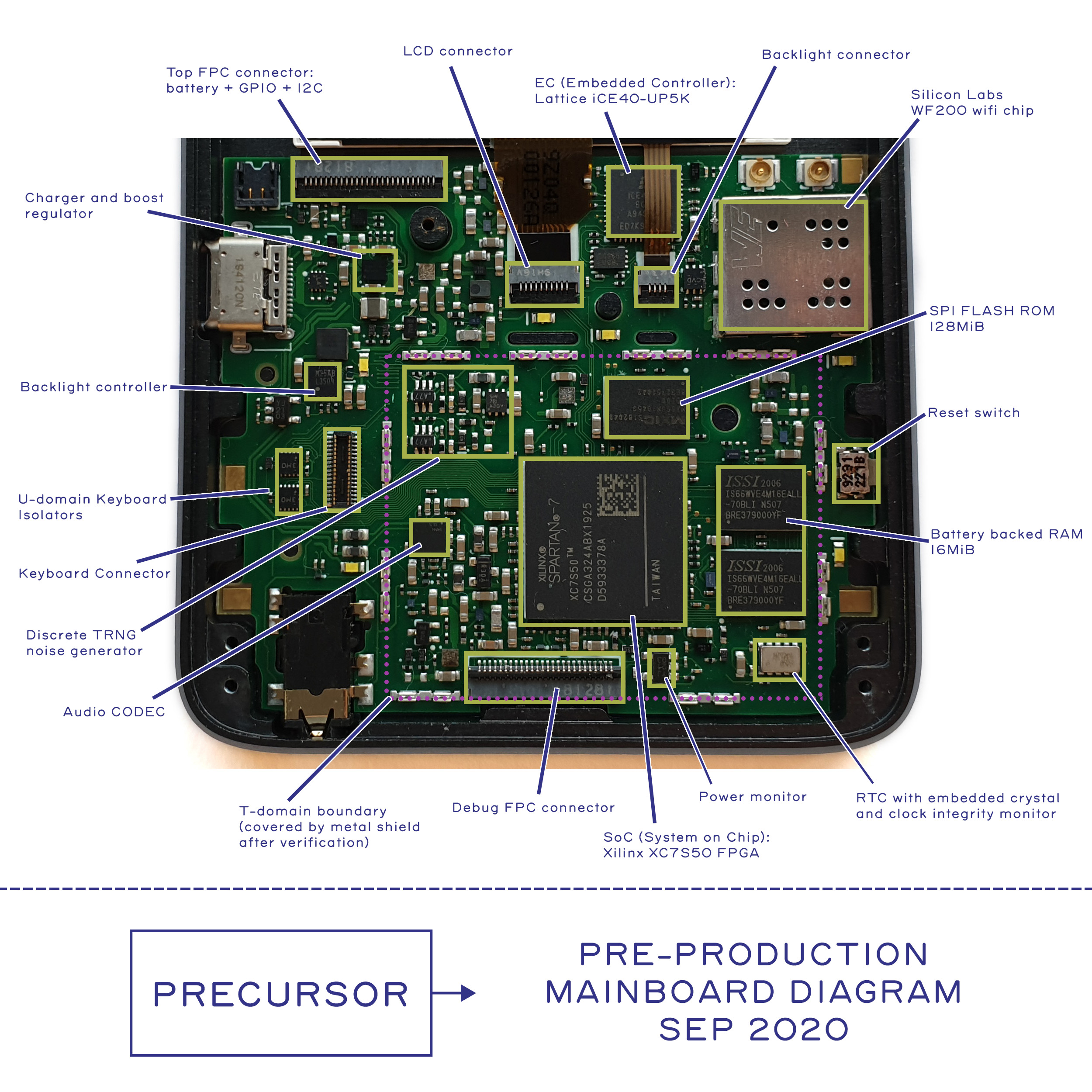
Despite the assurance from the likes of Google and Apple that our data is not vulnerable, we know deep down there are some uncertainties that we can’t control but precursors bridge that gap, Based on Scientific evidence that is measurable without access to a million-dollar microscope, users should be able to trust precursor. Among open hardware gadgets, the predecessor is also unique in that it was designed for portability from the ground up while most open FPGA hardware development boards share the evidence-based, compile your own CPU confidence properties of precursor, none of them are packaged in a compact, 7.2 mm, machined-aluminum shell, complete with a charger, a battery, a monitor and a keyboard, precursor draws less power than most FPGA because of the -1l variant Xilinx Spartan 7-series at its core, L for “low leakage” combined with a super-low-power Lattice iCE40 UP5K FPGA for deep-sleep system management and a Silicon Labs WF200 with integrated network co-processor for Wi-Fi connectivity — allows Precursor to achieve a standby time measured in days and an active screen time of about five to six hours.
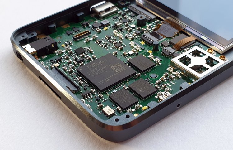
Precursor consists of the following major elements:
The Mainboard will be manufactured by AQS, an EMS provider, at their South Korea facility. The bare PCB will be produced by King Credie in Guangdong, China. All of the parts on the BOM were selected explicitly for ready availability in distribution channels such as Mouser and Digi-Key. We do anticipate a 12-week lead time on the Xilinx FPGAs, and acquiring them in a timely fashion represents a risk given the current pandemic and the status of the global supply chain.
The rear case and radome will be manufactured by Jiada, a contract mechanical engineering supplier located in Guangdong, China. Production rear cases will be manufactured on-demand using a CNC milling process and finished with anodization. The radome will be produced using an injection molding tool that will be opened upon the successful conclusion of the funding campaign.
The battery is sourced from a supplier in Guangdong, China. Because of its short shelf life and high MOQ, this does represent a high risk item. We will finalize the battery supplier and UN38.3 certifications that allow for air shipping after the conclusion of the campaign.
The front bezel is a step-milled, edge-beveled PCB made using a special FR-4 composition impregnated with black dye by King Credie in Guangdong, China. The front bezel also incorporates the Wi-Fi antenna.
The LCD is sourced from Sharp Microelectronics. Due to its highly critical nature and long lead time, we have gone ahead with a risk buy to ensure its availability for the campaign. If the campaign greatly exceeds volume expectations, we may have to take a staged approach to delivery as LCD shipments become available.
The backlight assembly was pre-manufactured to match the LCD.
The keyboard overlay is a full-custom, UV-cured, polycarbonate assembly with silkscreen printing, all done via AQS in Dongguan, China.
The keyboard PCB is a semi-custom “transparent” substrate, manufactured by King Credie in Dongguan, China.
The button array is sourced from AQS in Dongguan, China.
The final assembly will be done at AQS in South Korea.
The Precursor tier includes the following items in the box:
One fully assembled and tested Precursor device in an aluminum case, complete with display, bezel, QWERTY keyboard, and battery, and pre-loaded with low-level factory test firmware.
One “debug board,” which is a Raspberry Pi 3B+ or 4 HAT. This used for low-level debugging and reflashing of the Precursor in case you brick it. Raspberry Pi not included.
Three alternate keyboard overlays: QWERTZ, AZERTY, and Dvorak.
Press-fit metal shield for the trusted domain of the Precursor PCB (to be installed after verification).
Four grams of EPO-TEK 301 in a bi-pak, for sealing the metal shield Note: the seal is permanent and we can’t do any warranty returns/exchanges on sealed devices. Do not apply glue to active connectors.
The Limited Edition Precursor tier includes all of the above, with a special limited edition case. You will also receive the regular production aluminum case body as well, as a bonus spare part.
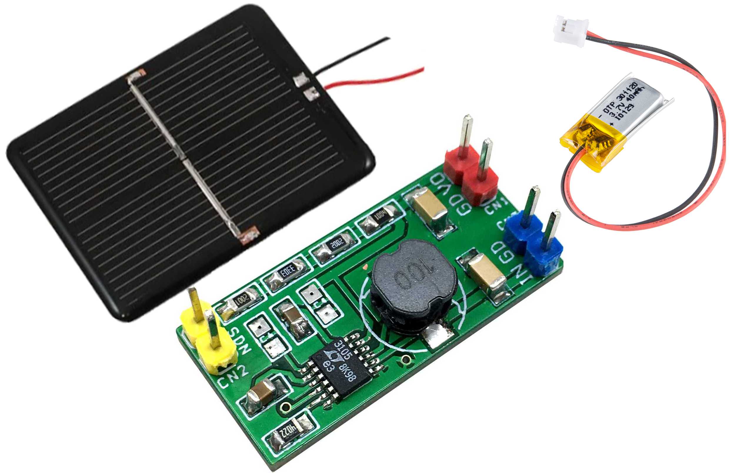
This is a tiny module that allows users to charge small Li-ion batteries, CR2032 or equivalent, from a low power source such as a small photovoltaic cell. The project consists of the LTC3105 step-up DC-DC converter chip which features Maximum Power Point Control (MPPC) and 250mV start-up voltage which enables operational directly from low power, high impedance alternative power sources such as photovoltaic cells. A user-programmable MPPC set point maximizes the energy that can be extracted from any power source. Burst Mode operation, with a proprietary self-adjusting peak current, optimizes converter efficiency and output voltage ripple overall operating conditions. The circuit works with single-cell or dual-cell in parallel. The operating supply of this project is as low as 225mV and a maximum of 5V. Input supply should not exceed 5V DC. The module is programmed to output 4.1V which is important to charge the Li-On battery. Jumper J1 should be open for normal operation, close to disable the output.
Photovoltaic Cell Battery Charger / Solar Cell Li-Ion Battery Trickle Charger with MPPC – [Link]
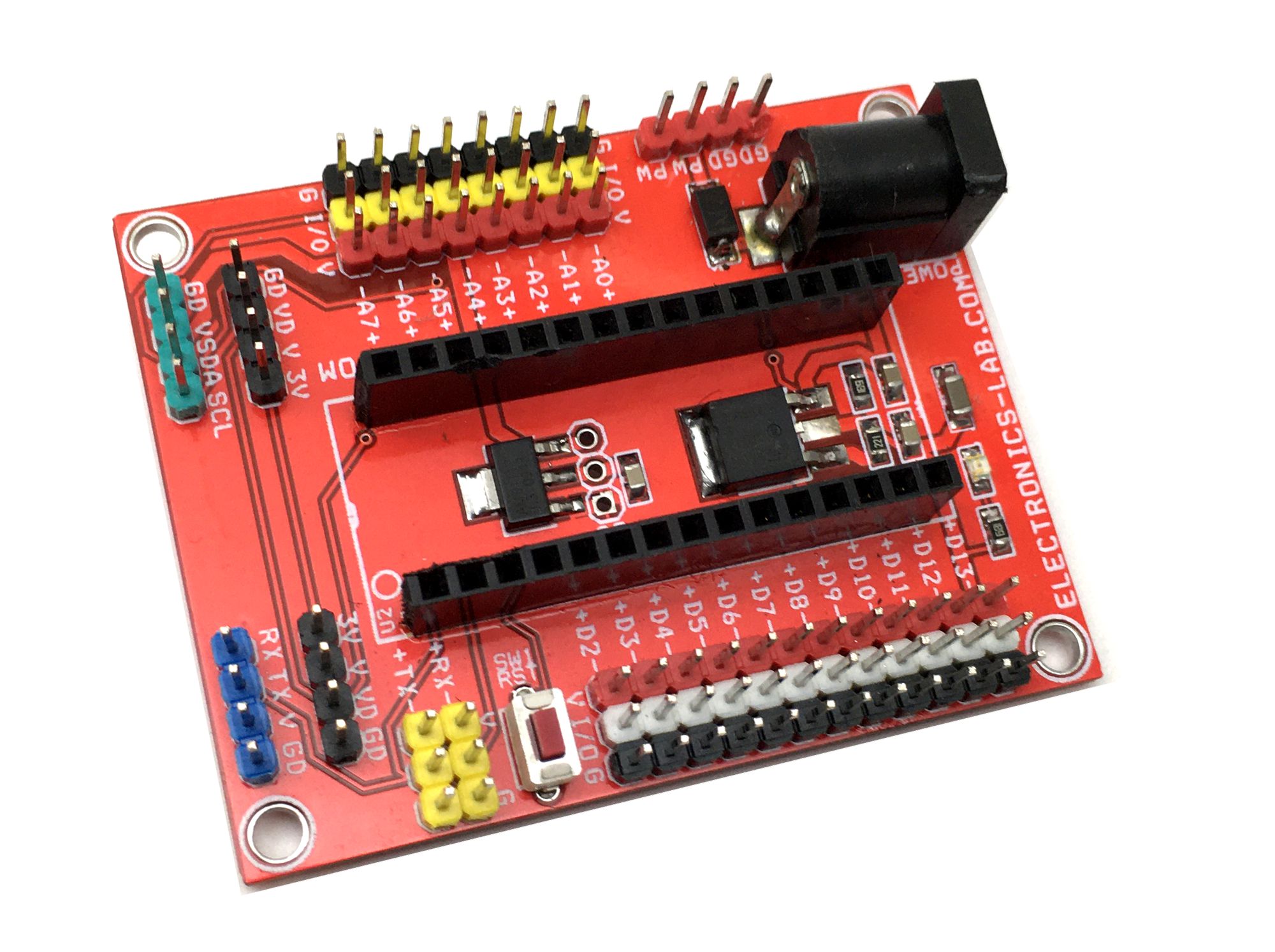
If you need to interface many devices and sensors to Arduino Nano, then, this project is for you. This is a Nano expansion I/O shield (breakout board) for the Arduino Nano. The board facilitates the easy connection between Arduino Nano and other devices. Each Arduino (I/O) Pin including the 5V DC and GND pins are available for easy connection to the sensors and other devices. The board enables the easy interface of many devices and sensors which includes various power voltage options. It provides several different options for power outputs and wide range of operating power supply input.
Expansion Shield – Breakout Board for Arduino Nano – [Link]