Choosing the Right Diode – Types and Uses Explained for Beginners

Diodes, essential in electronics, range from P-N junctions for AC to DC conversion, to Zener for voltage stability, and LEDs for lighting.

From small LED drivers to rectifiers to Switch Mode Power Supplies (SMPS), the diode is a key component in each of those everyday appliances. They are also used in charging LED indicators and reverse polarity protection circuits in router chargers and many more; diodes are used everywhere, but this little device often does not get much attention. So, in this article, we will learn what diodes are, how they work, and some applications of diodes.

We will also learn about WIN SOURCE, a leading electronic component distributor, that offers a wide range of diodes to assist customers in meeting the requirements of different applications. So, let’s begin our article by knowing about diodes.

What Is a Diode?

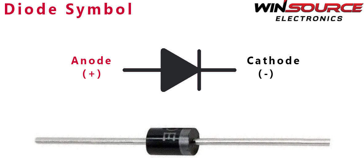
A diode is a simple two-pin electronic device that lets electricity flow mainly one way. It’s like a door that only opens in one direction, and if you try to open it in another direction the liver will not let you open it without breaking it. The diode has two sides. On one side it’s hard for electricity to get through and on the other side, it’s easy.

Diodes are very simple devices that make it easy to convert alternating current (AC) into direct current (DC) and protect gadgets from getting damaged by electricity going the wrong way. They’re mostly made from materials like silicon and germanium and have voltage and current ratings. Although all diodes work by allowing current to move in just one direction, the specific way they do this can vary. Based on this analogy, they can be divided into many different types.

Characteristics of Diode

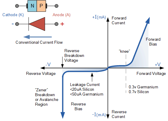
Diodes have three key characteristics based on how they are connected in a circuit: forward-biased, where they allow current to flow easily; reverse-biased, where they block current flow; and zero-biased, where they are not influenced by any external voltage and behave according to their natural properties.

Image Source: electronics-tutorials

Forward Biased

In a forward-biased diode, when a positive voltage is applied to the anode (P-side) and a negative voltage to the cathode (N-side), the diode becomes conductive. The voltage across the diode gradually reduces, and once it reaches a certain threshold called the forward voltage drop (typically around 0.6 to 0.7 volts for silicon diodes), the diode starts conducting heavily, allowing current to flow through it.

Reversed Biased

In a reverse-biased diode, when a negative voltage is applied to the anode (N-side) and a positive voltage to the cathode (P-side), the diode is in a non-conductive state, blocking the current flow. However, as the reverse voltage increases, a point is reached where the diode breaks down, and a small reverse current, known as the reverse saturation current, starts flowing. This breakdown voltage is called the Zener voltage in Zener diodes.
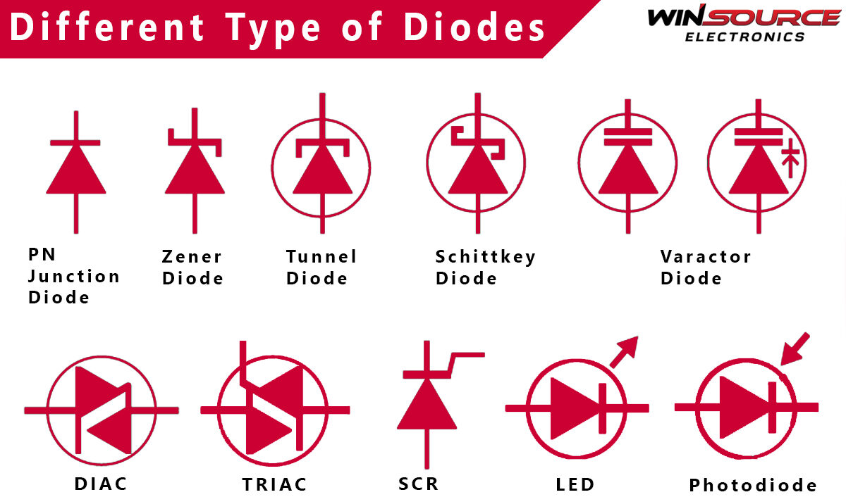
Types of Diodes

There are many different types of diodes available in the market, and the most common ones are the simple P-N Junction diode, other than that there are the Zener diode, Light Emitting Diode, Schottky diode, Laser diode, Diac, Triac, SCR and more. in this section of the article, we will talk about.
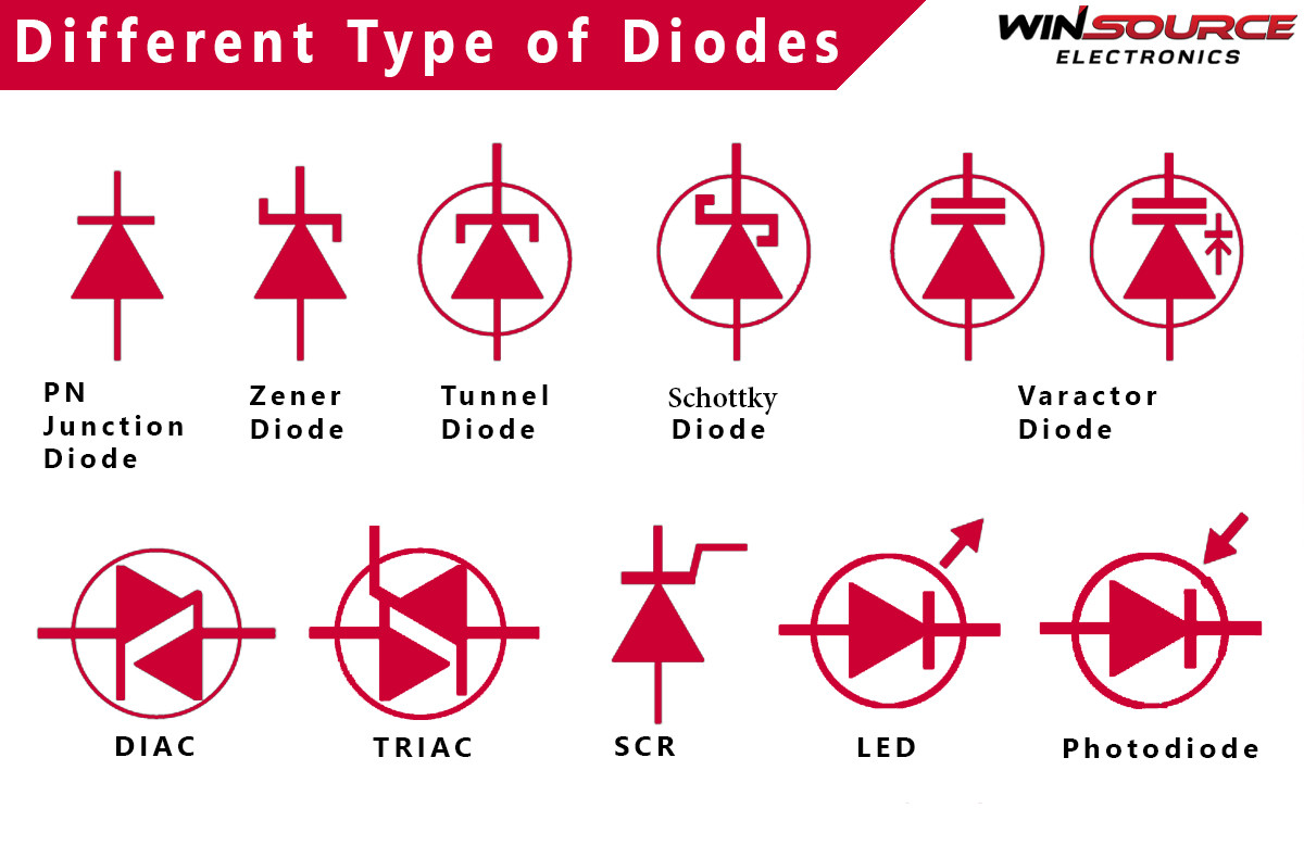
  1. P-N Junction Diode
  2. Zener diode.
  3. Light Emitting Diode
  4. Schottky diode
  5. Laser diode
  6. Diac
  7. Triac
  8. SCR

P-N Junction Diode

P-N junction diodes are basic components made by joining p-type material, which has lots of holes, with n-type material, full of electrons, to form what’s called a P-N junction. This setup allows for two main actions: diffusion and drift. In diffusion, holes from the p-side and electrons from the n-side move across to the other side, creating a flow of current. Then, drift comes into play when an electric field, caused by a layer of charged ions on each side, pushes electrons back to the n-side. This clever design makes sure that electricity mostly flows one way through the diode, which is useful for changing AC (alternating current) to DC (direct current) in many electronic devices. Some common examples of PN Junction diodes are 1N4001, 1N4003, 1N4007, STPS340U, PDU540-13 and more

Zener diode

Zener is a specially designed semiconductor device that works in the reverse direction, unlike a PN Junction diode which operates in a forward direction. With this characteristic, a Zener diode functions as a voltage regulation and protection device in electronic circuits. It ensures that the voltage across its terminals remains quite stable, making it a key component in applications requiring a consistent voltage reference or surge protection. Some common examples of Zener diodes are 1N3335B, 1SMB5914BT3, ZMM5253B-7, DDZ9715T-7 etc..

Light Emitting Diode (LED)

Led or Light Emitting Diode is a special type of semiconductor material or Diode that emits light when an electric current is applied in the forward direction. first discovered in 1907 by British experimenter H. J. Round. However, it wasn’t until the 1960s that LEDs were developed into a practical electronic component. The first was discovered in 1907 by British experimenter H. J. Round. However, it wasn’t until the 1960s that LEDs were developed into a practical electronic component. But it was not until the 1990s that the blue LEDs were invented. LED converts electrical energy directly into light, resulting in reduced energy consumption and longer lifespan.  Some common examples of Light Emitting Diode (LED) are SLR343WBC7T31XM, LN1471YTR, LB T66G-U1BA-59-Z, HLMP-BD06-P0000 etc.

Schottky diode

Schottky diodes have many switching sides and are used in SMPS as a reverse recovery or as a transition voltage impression diode. These diodes are known for their fast switching speed & low forward voltage drop. It is constructed using a metal-semiconductor junction instead of a traditional semiconductor-semiconductor junction. A unique design allows Schottky diodes to have a lower forward voltage drop compared to regular diodes & making them suitable for high-frequency applications and power efficiency. The absence of a P-N junction in their structure reduces recovery time, making Schottky diodes ideal for applications where fast switching is critical, such as in switching power supplies and RF (radio frequency) circuits. Some common examples of Schottky diode are 0SQ045NG, S110FP, SS15FA, NRVBS240LT3G etc.

Laser diode

Laser stands for Light Amplification by Stimulated Emission of Radiation. Lasers are a special type of semiconductor device that works on a principle similar to that of a light-emitting diode (LED). But it is designed to produce a highly concentrated & monochromatic beam of light. Unlike LEDs that disperse light, lasers harness the process of “stimulated emission,” where electrons in a material are excited to a higher energy level by an external energy source. When these excited electrons return to a lower energy level, they emit photons (light particles). These photons then stimulate other excited electrons to emit more photons, creating a chain reaction that produces a concentrated, coherent beam of light. The light coming out of this is very focused and can be used in many applications including optical communication, laser printing, barcode scanners & medical devices. Some common examples of Laser diodes are SPL PL90, RLD78MZM7-00A, 1054, SPL LL90_3 etc.

Diac

Diac stands for Diode for Alternating Current and is a semiconductor device known for its bidirectional conduction characteristics. Essentially, it can conduct current in both forward and reverse directions once a certain voltage threshold is reached. Discs are commonly used in triggering thyristors and TRIACs (Triode for Alternating Current), aiding in the control of AC power in applications like dimmer switches and phase-locked loops. Due to their symmetrical behavior & ability to trigger at specific voltage levels in both polarities, Diacs play a crucial role in facilitating controlled switching of AC circuits, ensuring precise and synchronized operation in a variety of electronic systems. Some common example of DIAC are DB3TG, HT40, HT40, K0900E70, MKP1V120RLG etc.

Triac

A TRIAC, or Triode for Alternating Current, is a type of semiconductor device that can control the flow of electrical power. It is similar to a relay but can handle much higher currents and voltages. A TRIAC has three pins: the Gate, the Main Terminal 1 (MT1), and the Main Terminal 2 (MT2).

The way it works is pretty straightforward. When a small voltage is applied to the Gate, it allows current to flow between the two main terminals, MT1 and MT2, regardless of the direction of the flow. This makes the TRIAC very useful for controlling AC (alternating current) power, where the direction of current changes regularly. Once the Gate receives the signal, the TRIAC stays on, letting power through until the current drops below a certain level or the AC cycle ends. TRIACs are commonly used in applications where you need to control devices like AC motors, Incandescent Light bulbs, or heating elements. Some common examples of TRIAC are  TIC236D, Q6025L6TP, BTA16-800BWRG, TMA254B-L etc.

SCR

An SCR, or Silicon Controlled Rectifier, is a type of electronic device used to control the flow of electricity. It’s a four-layer semiconductor that operates as a switch. The SCR has three pins: an anode, a cathode, and a gate. When no voltage is applied to the gate, the SCR blocks current from flowing through it, acting like an off switch. However, when a small voltage is applied to the gate, it allows current to flow from the anode to the cathode, turning the switch on. Once on, the SCR will stay on even if the gate voltage is removed, as long as there is current flowing through it. To turn it off, the current flowing through the device must be interrupted. SCRs are widely used in power control applications like dimming lights, controlling motors, and power conversion systems because they can handle high voltage and current levels efficiently. Common examples of SCR are TN1605H-6T, C106D, S6015L, BTW69-600, TYN1225RG etc.

In this article, we’ve explored the world of diodes, from the basic P-N junction diodes that guide electricity in one direction, to specialized ones like Zener diodes for voltage regulation and protection, and LEDs that light up our devices. We also touched on advanced types like laser diodes, used in high-tech applications, and power control devices like SCRs and TRIACs. Diodes may seem small and simple, but they play huge roles in making our electronic devices work smoothly and efficiently.

CH32V003 USB Development Board: An Affordable and Versatile Platform for USB Peripheral Projects

CH32V003 USB top view

LECTRONZ has introduced a new USB Development Board called CH32V003. It’s designed for people who like to tinker with RISC-V microcontrollers. The main part of the board is a microcontroller with part no CH32V003F4U6 made by WCH. It can run at speeds up to 48MHz, has 16KB of storage for programs, and 2KB of memory for data.

The board comes with a crystal installed, which helps with timing, but you can take it off if you want and use a different method for timing. This gives you flexibility in how you set up the clock for your projects.

It has 18 pins that you can connect things to, and 13 (or 15 if you count the crystal pins) of them are easy to reach from the sides. There’s also a light (LED) that you can control at pin PC0 and a button at pin PD7, which can also be used to reset the board. It’s a handy and versatile tool for people who like to experiment with microcontrollers.

The product page highlights that the CH32V003 USB Development Board is capable of using a technique called “bitbanged USB” with the rv003usb stack by CNLohr. This makes it easy for users to plug in the board and use it for USB-related projects. Three out of the 18 available pins on the board are specifically set up for USB functions, and you can access the USB data lines through holes on the inside of the board.

The board is fully compatible with the CH32V003FUN project, which is open-source. The design of the printed circuit board (PCB) is also open source, meaning its design details are freely available with the CERN-OHL-W-2.0 license on GitHub.

To program the board, users need a compatible SWIO programmer, such as the WCH LinkE. Alternatively, other programmers like the ESP32-S2 can be used, as described in the documentation.

For Arduino enthusiasts, the Ardulink project can be used to program the board with an AVR-based ATMega328P device, like those found in Uno R3 or Nano boards.

The CH32V003 USB Development Board is mainly designed for development and evaluation purposes. It is priced at $5.16 for a single unit, and there are discounts for larger quantities; for example, two units cost $5.58, three units cost $6.42, and so on.

Introducing NRFICE: A Bluetooth FPGA Board for Edge Computing and IoT Applications

The NRFICE FPGA is a Bluetooth FPGA board designed for edge computing and IoT applications. It is built upon a combination of the dual-core nRF5340 Bluetooth SoC and the Lattice ICE40UP5K FPGA.

The NRFICE is a Bluetooth FPGA board designed to be compatible with the Arduino UNO form factor. It combines two key components: the dual-core nRF5340 Bluetooth SoC and the LatticeICE40UP5K FPGA.

The Lattice ICE40UP5K FPGA is known for its low power consumption and high performance, making it suitable for edge computing and artificial intelligence projects. On the other hand, the nRF5340 Bluetooth SoC is a versatile chip that supports various communication protocols such as Bluetooth Low Energy (BLE), Bluetooth Mesh, Thread, NFC, and Zigbee.

What sets NRFICE apart is its ability to directly load a project into the ICE40 FPGA through the nRF5340 chip. This eliminates the need for complex toolchain setups typically required for FPGA development. As a result, NRFICE enables a new approach to FPGA development, where users can host bitstreams in the cloud, select them using a mobile device, and wirelessly load them onto the board.

This innovative feature opens up possibilities for seamless and flexible FPGA development, allowing users to focus more on their projects and less on setup and configuration tasks.

The NRFICE FPGA is a Bluetooth FPGA board designed for edge computing and IoT applications. It is built upon a combination of the dual-core nRF5340 Bluetooth SoC and the Lattice ICE40UP5K FPGA.

The NRFICE Bluetooth FPGA board comes with a built-in J-Link OB for easy debugging and programming, eliminating the need for emulator dongles. It supports Arduino Uno 3.3V shields and has a 5V power supply onboard, allowing it to power shields and daughterboards for various applications like LED lighting and motor control.

Key Specifications:

  • Microcontroller: Nordic Semiconductor nRF5340, dual-core Bluetooth 5.3 SoC with 128MHz Cortex-M33, 1MB Flash, and 512KB RAM.
  • FPGA: Lattice Semi ICE40UP5K with 5280 LUTs, 1024KB single-port RAM, and 120KB embedded block RAM.
  • Network Capabilities: Bluetooth Low Energy, Bluetooth 5.3, LE Audio, direction finding, Bluetooth mesh, Thread, Zigbee, 802.15.4, and more.
  • Buttons and LEDs: Reset buttons for ICE40 and nRF, user-programmable buttons, and RGB LEDs for status indication.
  • USB Connectivity: USB-C for J-Link OB and nRF5340, providing VCOM serial port and other USB implementations.
  • Power Supply: 9V – 12V via a barrel power connector, 5V @ 3A regulator.
  • Form Factor: Arduino Uno is compatible with a 0.1” pinout.

NRFICE is an open-source project certified by OSHWA, offering access to its Bill of Materials, schematics, Gerber files, Verilog projects, and more on GitHub. It works with an open-source Android app for wireless programming and configuration of the nRF5340 chip and ICE40 FPGA. Additionally, professional development tools like Segger Embedded Studio and Lattice’s Radiant are available for free.

The NRFICE FPGA board is priced at $159 with free shipping within the US and a $12 shipping fee worldwide. The campaign on Crowd Supply has surpassed its funding goal, and orders are expected to ship by August 2, 2024.

Introducing Arduino Nano 33 BLE Rev2: Enhanced Hardware and Performance Upgrades

The Arduino Nano 33 BLE Rev2 is an updated version of the popular Arduino Nano 33 BLE board. It has several improvements, including dual-IMU (Inertial Measurement Unit) support for better motion sensing, an upgraded power supply for improved performance, and other enhancements. Despite these upgrades, it maintains the same size and shape as the original Nano 33 BLE, making it an easy and seamless upgrade for users familiar with the older version.

The Arduino team praises the Nano 33 BLE for being highly popular and versatile. They highlight its compact size, compatibility with 3.3V systems, built-in nine-axis IMU (Inertial Measurement Unit) for motion sensing, powerful processor, Bluetooth Low Energy module for wireless communication, internal antenna for data transmission using ArduinoBLE library, and compatibility with MicroPython programming.

“These updates collectively contribute to a more streamlined and robust device, ready for you to test and build just about any IoT [Internet of Things] project – and more,” the Arduino team claims.

The Arduino Nano 33 BLE Rev2 maintains the same size as the original version, but some hardware changes may require sketch adjustments. The major change is the use of two separate inertial measurement units (IMUs) instead of a single nine-axis unit. The new IMUs include the Bosch Sensortec BMI270 six-axis IMU and BMM150 three-axis magnetometer.

The power circuitry has also been upgraded to the Monolithic Power MP2322 step-down converter, promising improved performance. The board also features a VUSB solder jumper for enabling the VUSB pin, along with new pads and test points for accessing USB, SWDIO, and SWCLCK signals.

However, the board’s processor remains unchanged: the Nordic Semiconductor nRF52840, which offers a 32-bit Arm Cortex-M4 core running at up to 64MHz, 256kB of static RAM (SRAM), and 1MB of flash storage. These specifications ensure powerful processing capabilities for various applications.

The board retains the footprint of the original, though now includes pads for USB, SWDIO, and SWCLCK signals. (📷: Arduino)
The board retains the footprint of the original, though now includes pads for USB, SWDIO, and SWCLCK signals.

The Arduino Nano 33 BLE Rev2 is now available to order on the Arduino store priced at $24.17 — or $26.92 to have the bundled pin headers pre-soldered.

SparkFun Introduces ESP32-C6 Thing Plus: Revolutionizing IoT Projects

The SparkFun ESP32-C6 Thing Plus is expected to bring significant advancements to IoT projects due to its user-friendly design, advanced features, and seamless connectivity capabilities.

Located in Boulder, Colorado, SparkFun Electronics has officially launched the ESP32-C6 Thing Plus, a wireless development board that promises to be a game-changer in the industry. This board is designed to enhance the functionality and performance of your projects significantly. SparkFun’s extensive experience of over eight years in working with Espressif’s technologies has culminated in the development of the ESP32-C6, marking a major achievement in their roadmap for creating development boards based on ESP modules.

In essence, the ESP32-C6 Thing Plus from SparkFun is set to revolutionize IoT projects by offering a well-designed, feature-rich, and seamlessly connected platform for developers and enthusiasts.

Packed with cutting-edge technology and housed in a compact, user-friendly footprint, the SparkFun ESP32-C6 Thing Plus empowers your wireless creations like never before.

The SparkFun ESP32-C6 Thing Plus is a compact and easy-to-use development board for IoT projects. It’s powered by the ESP32-C6 WROOM-1-N16 module from Espressif™, which has a strong RISC-V single-core processor, plenty of flash memory, and various wireless options like 2.4 GHz WiFi 6, Bluetooth® 5.3, Zigbee, and Thread (802.15.4)

“We’re thrilled to introduce the SparkFun Thing Plus – ESP32-C6,” says Kirk Benell, CTO at SparkFun Electronics. “This board combines performance, affordability, and ease of use, empowering makers to bring their next-generation IoT projects to life. It underscores our commitment to offering comprehensive development board solutions for all skill levels and project needs.”

Here are some key features and benefits of this board:

  • Expandable Storage: It has a slot for a microSD card, so you can easily add more storage to your projects.
  • Integration with Sensors: The Qwiic connector lets you easily connect to SparkFun’s range of sensors and devices.
  • Efficient Power Management: It comes with a LiPo battery charger and fuel gauge, making power management more efficient. You can power and program it using USB-C or a LiPo battery with the 2-pin JST connector.
  • Versatility: This board is Feather-compatible, meaning it can fit into various setups and configurations.
  • GPIO Pins: You can access all 23 GPIO pins of the ESP32-C6 through 0.1in.-spaced PTH headers, giving you flexibility in your project designs.

You can find detailed information about SparkFun’s Espressif boards, including specifications, features, and compatibility, on their official website at https://www.sparkfun.com/pages/espressif

For more information about SparkFun Electronics as a company, including its history, mission, and values, you can visit its “About Us” page at www.sparkfun.com/about_sparkfun. This page typically provides insights into their journey, team, commitment to education, and their role within the maker and electronics communities.

Analog Discovery Pro ADP2230 – USB Oscilloscope with Waveform Generator, Logic Analyzer, and Variable Power Supply Available for $749.00

Analog Discovery Pro ADP2230 mixed-signal oscilloscope & waveform generator with 16 digital I/O, dual power supplies, and USB 3.0 for advanced tasks

The ADP2230 has 16 digital input/output channels that work with 3.3 V CMOS, can sample up to 125 MS/s, and buffer up to 128 MS per channel. It also includes an analog output channel with a 15 MHz bandwidth and 14-bit resolution, capable of producing standard, modulated, and custom waveforms.

Additionally, it has two programmable power supplies with a range of 0.5 V to 5 V (positive) and -0.5 V to -5 V (negative), each providing up to 1 A or 3 W. For connectivity, it uses USB 3.0 for fast data transfer and has BNC connectors for oscilloscope probes, connecting to computers via a USB Type-C to C cable. The device also features advanced triggering options, including triggers from analog channels, a function generator, digital I/O, and external sources, with modes like auto, manual, and single. These triggers work with both analog and digital inputs and offer edge, level, and pattern options.

Analog Discovery Pro ADP2230 Specifications:

  • Model: Analog Discovery Pro ADP2230 USB Mixed Signal Oscilloscope with deep memory buffers for long acquisitions
  • Analog Inputs:
    • Two BNC input channels
    • 14-bit resolution, ±25 V input range
    • 50+ MHz bandwidth, up to 125 MS/s per channel
    • 64 MS on-device buffering by default, expandable to 128 MS
  • Analog Output:
    • One BNC output channel
    • 14-bit resolution, ±5 V output range
    • 15 MHz bandwidth, up to 125 MS/s
    • Supports standard, modulated, and custom waveforms
  • Power Supplies:
    • Two programmable outputs (0.5 V to 5 V, -0.5 V to -5 V)
    • Up to 1 A or 3 W per channel
    • Hardware monitoring of system temperature, voltage, and sourced current
  • Digital I/O:
    • 16 3.3 V CMOS digital input/output channels
    • Sampling up to 125 MS/s
    • On-device buffering up to 128 MS per channel
    • Supports multiple communication protocols
  • Advanced Triggering:
    • Trigger sources: analog channels, function generator, digital I/O, external triggers, manual button
    • Modes: None, auto, manual, single
    • Analog trigger options: edge, pulse, transition, condition, level, hysteresis, hold-off
    • Digital trigger options: edge, level, pattern, glitch, protocol
  • Connectivity:
    • USB Type-C to C connection
    • USB 3.0 for high-speed data transfer
  • Software Support:
    • WaveForms application for Windows, Mac, Linux
    • WaveForms SDK for custom applications
    • LabVIEW and MATLAB compatibility
  • Additional Features:
    • Adjustable system clock, external clocking support
    • Cross-triggering between instruments
    • Internal hardware loopbacks
    • Optional control over power supplies via waveform generator
    • Network and Spectrum analysis tools
  • Physical Specifications:
    • Dimensions: 134.2 mm × 144.0 mm × 37.9 mm
    • Weight: 464 g
    • Product Compliance: HTC: 8471809000, ECCN: 3A992.a

In terms of software, the company said that the device supports WaveForms which is a free, user-friendly software for the ADP2230, allowing users to capture, record, analyze, and generate waveforms on their computers. Compatible with Mac, Windows, and Linux, it connects via USB or Ethernet. WaveForms includes tools like an oscilloscope, waveform generator, and spectrum analyzer, and offers a demo mode for testing without hardware. Additionally, it supports custom scripting in JavaScript and is compatible with Python, C, LabVIEW, and MATLAB for further customization.

Inside the box of the Analog Discovery Pro ADP2230, you’ll find a comprehensive set of accessories including a USB C to C cable, and a 5V 4A switching power supply with US and EU plug adapters. For oscilloscope functionality, it comes with a pair of BNC x1/x10 Probes. The package also contains a 5-pack of 6-pin Headers & Gender Changers and a 2×16 flywire for various connection needs, along with a Flywire label sheet for easy identification.

The Analog Discovery Pro ADP2230 is priced at $749.00 and is available on the Digilent website.

ILabs’ New RP2040 Connectivity Board Features u-blox SARA-R412M LTE (Cat M1/NB-IoT) and ESP32 Modules

 ILabs' RP2040 Connectivity Board Integrating SARA-R412M LTE, with RP2040 and ESP32-C3FN4 WiFi/BLE for diverse IoT projects.

ILabs’ RP2040 Connectivity Board is an RP2040-based development board with u-blox SARA-R412M for LTE (Cat M1/NB-IoT) and Espressif’s ESP32-C3FN4 for WiFi/BLE, designed for versatile IoT applications from remote monitoring to smart connected devices.

We’ve covered various connectivity boards like the SparkFun LTE Stick, and the Walter ESP32-S3, but the RP2040 Connectivity Board is unique as it combines an ESP32 and RP2040, offering the best of both worlds.

The board features Espressif’s ESP32-C3FN4 chip, providing advanced Wi-Fi and BLE. It’s powered by a RISC-V core with 4MB flash and 408KB SRAM and includes the ESP-AT interpreter for diverse network functionalities. It’s energy-efficient, with a 500mA battery charger, and has user-friendly reset and UF2 buttons, plus options for both onboard and external antennas.

It also includes the SARA-R412M module for LTE (Cat M1/NB-IoT), offering worldwide coverage and strong security features. This module connects to the RP2040 via a hardware serial port for fast data transfer and has an easy-to-install cellular antenna with a U.FL connector.

For network access, the board requires a nano SIM card. Users can choose their own SIM or opt for the 1NCE prepaid card, which provides 120 months of global connectivity for 150 SEK, including 500 MB of data and 250 SMS. The provided SIM card is meant for evaluation; for more features, users can directly contact 1NCE.

ILabs’ RP2040 Connectivity Board Features and Specifications:

  • High-Performance Microcontroller: Features RP2040 from Raspberry Pi, with dual-core Cortex M0 processor at 133MHz, 8 MB FLASH memory, and 264 Kb integrated RAM.
  • LTE Connectivity: Includes SARA-R412M module for LTE (Cat M1/NB-IoT/eGPRS) with international coverage and advanced IoT security features.
  • WiFi/BLE Capabilities: Integrated ESP32-C3FN4 chip supporting various Wi-Fi modes, Bluetooth LE, Bluetooth 5, and mesh capabilities.
  • USB Type-C Interface: Modern USB Type-C port for enhanced durability and compatibility.
  • BConnect Interface Connector: Allows for connecting a wide range of peripherals.
  • Power Efficiency: Low power supply design and onboard LiPO battery charger capable of 500mA for rapid charging and extended battery life.
  • User Interface: Two buttons for easy reset and UF2 mode activation, flexible antenna options with on-board chip antenna or U.FL connector.
  • Nano SIM Card Slot: Supports various prepaid SIM card options including 1NCE IoT Flat Rate.
  • Versatile Applications: Ideal for projects like remote monitoring systems and smart connected devices.
  • Arduino Compatibility: User-friendly programming compatible with Arduino, supported by comprehensive guides.
  • Expansion Capabilities: 26-pin expansion header for connecting sensors, buttons, and various devices.
  • Durable and User-Friendly Design: Equipped with a durable USB Type-C interface and user-friendly buttons for easy operation.

The board features a USB Type-C interface, a BConnect connector for peripherals, a built-in LiPO battery charger, and a 26-pin header for connecting sensors and devices. It supports Arduino programming, with detailed guidance on Earle F. Philhower’s GitHub and ILABS’ instructions. Programming the board is simplified due to its compatibility with Arduino. Detailed instructions can be found on Earle F. Philhower’s GitHub page and ILABS’ instructional pages.

The RP2040 Connectivity Board is available for purchase for 795.00 Swedish Krona, which is roughly equal to $77.79 in US dollars. This price offers value for its wide range of features and capabilities in the IoT sphere.

Particle Announces M-Series Muon Dev Board Featuring LoRaWAN and Satellite Connectivity Options

Particle unveils the M-Series Muon Dev Board, integrating Wi-Fi, cellular, LoRaWAN, and satellite in one unit, based on the M-SoM module.

Particle has recently announced its multi-radio modules with support for Wi-Fi, cellular, LoRaWAN, and even satellite communications on a single device, which we have covered in our M-SoM modules article, but what we haven’t written about is the Muon Dev Board which is the dev board that holds the M-SoM module.

The Muon is the Particle’s latest development board which integrates radios like LoRaWAN, Cellular, Wi-Fi, BLE, and GNSS, utilizing an RTL8722DM MCU and an Arm Cortex-M33 CPU. It’s designed for streamlined development and scaling in IoT applications, from prototyping to deployment.

Particle’s founder and chief executive officer Zach Supalla Explains:

There are other wireless technologies available. There are satellite networks that can reach far away places — but they don’t work indoors. There are sub-GHz networks like LoRaWAN that can penetrate deeper into buildings, but they only work where gateways have been connected. No one radio can exceed 85%. Well, how about all the radios? That, my friends, we can do.

M-Series Muon Dev Board Specifications:

  • Connectivity
    • Expansion Card interface for general-purpose input/output (GPIO) connectivity
    • Qwiic connector
    • LoRa module
  • Power via
    • USB-C with Power Delivery (PD),
    • Screw block for direct power source connections (5-12V), or
    • Lithium-polymer (LiPo) battery
  • Form Factor – Credit-card-sized carrier board with onboard M-SoM

According to Particle, the Muon Dev Board offers two major advantages, The first is Network diversity which eliminates the need for multiple devices with different radios, as the device can connect to any available wireless network without prior knowledge of the networks. With network redundancy and failover, devices can connect to several networks at once. The Particle platform guarantees event publication, no matter the connection. If one network fails, the device automatically switches to another to ensure data transfer to the cloud.

Particle is set to launch the M-series in three versions: the M-SoM, a multi-radio system-on-module; the Muon, a multi-radio development board designed for quick prototyping; and the Monitor M, a multi-radio industrial gateway.

You can now pre-order the M-Series Muon Dev Board for $49. The models featuring Wi-Fi, cellular, and LoRaWAN are expected to be shipped in the second quarter of 2024, whereas those including satellite connectivity will follow in the third quarter.

Pimoroni’s NVMe Base Duo Brings Dual SSD Support to the Pi 5

Pimoroni's NVMe Base Duo offers dual M-key SSD support (2230-2280) and PCIe Gen 2 speed, ideal for Pi 5 media centers and servers.

Pimoroni’s NVMe Base Duo for Raspberry Pi 5, features dual M-key NVMe SSD that supports 2230 to 2280 SSDs while utilizing PCIe Gen 2 technology for fast storage speeds. With dual SSD support, this device is built for media centers and server applications.

A few months ago, Pimoroni released the Pimoroni NVMe Base that can support a single SSD. Now, with the introduction of this new board, users can connect dual SSDs to the Pi 5. This isn’t the first dual SSD board; previously, Geekworm released the X1004 HAT+, which also offered dual SSD support.

The NVMe Base Duo utilizes PCIe Gen 2 technology for fast storage access, suitable for file servers or media centers, with a throughput of around 450MB/sec. Its compact design allows mounting above or below the Raspberry Pi 5, stabilizing with rubber feet and connecting via a PCIe Flex cable.

Pimoroni’s NVMe Base Duo Specifications:

  • NVMe Base Duo: PCIe Gen 2 extension board for Raspberry Pi 5, supporting two M-key NVMe SSDs (2230-2280).
  • Usage: Ideal for fast storage tasks like file servers, media centers, or high IOPS workloads.
  • Mounting and Design: Compact, mountable above or below Raspberry Pi, includes ‘PCIe Flex’ cable and rubber feet.
  • Performance: Offers about 450MB/sec total throughput, around 220MB/sec per disk.
  • Compatibility: Works with updated Raspberry Pi OS and firmware; compatible with a range of tested SSDs.
  • Bundles: Available alone or with 500GB (2x250GB) or 1000GB (2x500GB) SSDs.
  • Tested SSDs: Includes brands like Samsung, Crucial, and Kingston.
  • Limitations: Can’t boot Raspberry Pi 5 from NVMe drives due to firmware restrictions.
  • Product Variations: Minor differences are possible in the final product, but core features remain the same.

One little problem with most of these types of HAT is that the NVMe Base Duo can’t currently boot the Raspberry Pi 5 from its attached SSDs due to firmware limits, but this may change with future updates. Users should keep their Raspberry Pi OS and firmware updated to use all features.

The NVMe Base Duo package includes the PCB with two M-Key M.2 slots, a ‘PCIe Flex’ flat flex cable for connection, and four rubber feet for stability. For mounting, it comes with a set of hardware: four M2 bolts and two 5mm standoffs for SSD mounting, four 12mm M2.5 standoffs and eight short M2.5 bolts for the base, and four 20mm M2.5 bolts for ‘pass-thru’ mounting with a HAT.

The NVMe Base Duo alone costs £30, while bundled versions with 500GB (2x250GB) and 1000GB (2x500GB) SSDs are available for £91.80 and £115.50, respectively. At the time of writing the HAT is available for pre-order and it’s expected to ship around mid-April 2024.

AAEON’s VPC-5640S Drives Innovation for Embedded In-Vehicle Solutions

Power, ruggedness, and versatility put the VPC-5640S in poll position in the race for the in-vehicle application market.

AAEON, a leader in embedded edge platforms, introduces the VPC-5640S, a Multi-PoE & Fanless Appliance powered by the 12th Generation Intel® Core™ i7-1265UE Processor. The company has indicated that the VPC-5640S is a statement of intent in its pursuit to establish a strong base in the embedded in-vehicle solutions market.

The potential of the VPC-5640S is immediately obvious by the inclusion of four PoE LAN ports running at 2.5GbE speed (IEEE802.3 at/af), alongside an additional standard RJ-45 for Intel® Ethernet Controller I226-LM, also at 2.5GbE. While the remainder of its front panel I/O is relatively standard for an embedded PC such as the VPC-5640S, with two USB 3.2 Gen 2 and two USB 2.0 ports, its rear panel possesses a number of interfaces that facilitate process control and task execution functions conducive to video surveillance applications.

The VPC-5640S rear I/O provides three DB-9 ports, two of which are for RS-232/422/485, while the third is for dual Isolated CANBus FD function. Joining these is a DB-15 port for an 8-bit digital I/O, two HDMI 1.4b, and a DIP switch. Four SIM card slots introduce the machine’s expansion capabilities, with Wi-Fi being made available via an M.2 2230 E-Key and two M.2 3052 B-Keys, which can utilize two of the machine’s four SIM slots to host two 5G modules simultaneously. The VPC-5640S contains adequate storage provisions via a 2.5” HDD for SATA at 6Gb/s, along with NVMe thanks to its M.2 2280 M-Key.

AAEON have noted the system’s potential as a fleet management solution, and its rugged features and onboard GPS, NEO-M9V & G-Sensor functions certainly support this notion, being designed for optimum functionality in the harshest settings. The VPC-5640S has a wide -40°C ~ 70°C temperature and 9V ~ 36V DC power input range, with the crucial addition of circuit protection and ignition delay on/off, which serves to protect crucial data against failure caused by variations in environmental conditions and power supply fluctuations. The VPC-5640S is also E-Mark certified, fanless, and boasts MIL-STD-810H vibration and shock tolerance.

“Exploring new vertical markets is always part of our roadmap, and we feel that in the VPC-5640S, we have produced a truly elite in-vehicle system,” said Louis Wu, Product Manager for AAEON’s Smart Platforms Division. “With its exceptional ruggedness and very targeted selection of interfaces, we hope to see this be a game-changer for our customers”.

AAEON note that while the VPC-5640S comes equipped with the 12th Generation Intel® Core™ i7-1265UE Processor by default, SKUs using the Intel® Core™ i5-1245UE and Intel® Core™ i3-1215UE are also available on a project basis.

The VPC-5640S is now available for order via AAEON’s contact form.

For more information about the VPC-5640S, please visit its product page.

TOP PCB Companies