Laird has introduced Sentrius™ MG100 micro-gateway with LTE-M/NB-IoT and Bluetooth 5
Based on Laird Connectivity’s Pinnacle 100 modem, the Sentrius MG100 Gateway captures data from Bluetooth 5 sensors and sends it to the cloud via a global low power cellular (LTE-M/NB-IoT) connection. Supports LTE bands 1, 2, 3, 4, 8, 12, 13, 20, and 28.Based on the Sierra Wireless HL7800 module, the MG100 includes Bluetooth 5 features like CODED PHY, 2M PHY, and LE Advertising extensions.
Key features
Wireless connectivity
Flexible power options
Certified for global deployment
Antenna choices
Additional features
LTE-M / NB-IoT radio via Sierra Wireless HL7800 module (Chipset: Altair ALT1250)
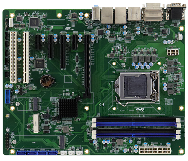
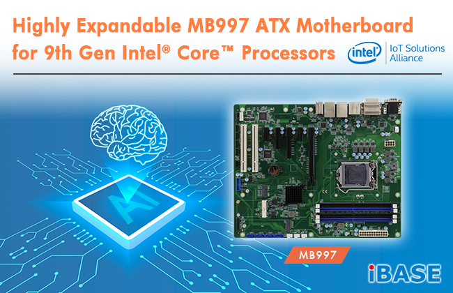
IBASE Technology Inc., a leading manufacturer of industrial motherboard and embedded systems, has rolled out the MB997 ATX motherboard for 9th Gen Intel® Core™ i7/i5/i3 and Xeon® processors. The Intel® C246/Q370/H310-based motherboard is designed for diverse applications, such as industrial automation, AI integrated systems, and smart retail systems.
The latest MB997 delivers high-performance computing for demanding industrial applications while providing multiple connectivity, expansion and functionality to meet customer requirements. The board supports up to 7 expansion slots including 1x PCI-E(x16), 1x PCI-E(x8)/Gen3.0, 1x PCI-E(x4), 2x PCI-E(x1), and 2x PCI, as well as 6x USB3.1, 2x USB 2.0, 2x SATA 3.0, and 6x COM ports. It can handle up to 128GB DDR4 memory across four slots and support three independent outputs (HDMI 2.0a, DVI-D, and DisplayPort) with 4K resolution each.
The board is loaded with advanced features such as TPM (2.0) hardware-based security to ensure platform integrity, iSMART 4.0 technology that enables power saving, power on/off and power resumption, and also NVMe and CNVi interfaces that bring various performance improvements. Like all IBASE industrial motherboards, MB997 comes with strict revision control, modification control and long-term support. Operating systems supported are Win10 IoT Enterprise and Linux Ubuntu.
MB997 FEATURES:
9th Gen Intel® Xeon® E / Core™ i7/i5/i3 processors
4x DDR4 DIMM, Max.128GB
Intel® processor integrated graphics supports HDMI(2.0a), DVI-D, and DisplayPort
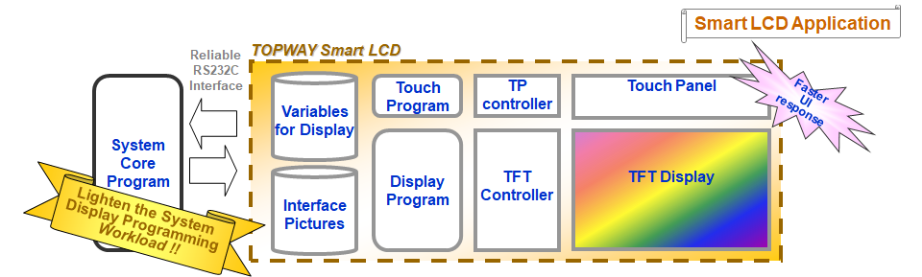
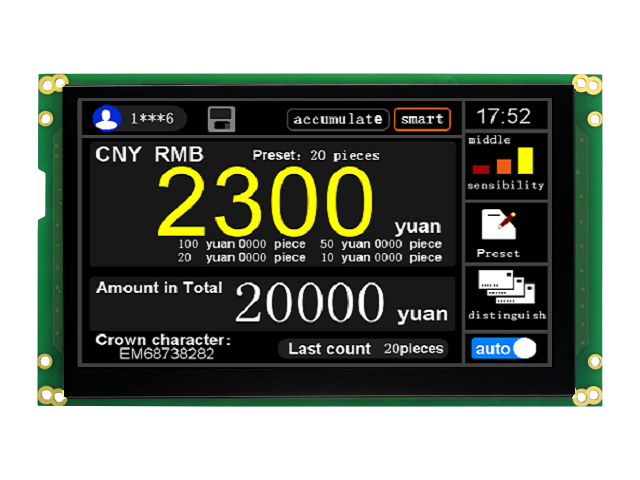
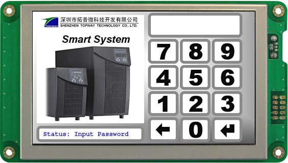
Shenzhen Topway Technology Co.Ltd. has launched their TOPWAY Smart TFT LCD module, which embeds LCD driver, controller and MCU, in a color LCD module with digital brain. A thin-film-transistor liquid-crystal display (TFT LCD) is a variant of a liquid-crystal display (LCD) that uses thin-film-transistor (TFT) technology to improve image quality such as brightness and contrast.
A TFT LCD is an active matrix LCD, in contrast to passive matrix LCDs or simple, direct-driven LCDs with a few segments. Smart TFT LCD sets engineer free from tedious display programming, so that product engineer can focus on product development. Smart TFT LCD module can help users greatly reduce product’s time-to-market. And the product is more reliable with high EMI tolerance.
Taking over the duty of displaying content and respond to touch event, Topway launched Smart LCD module couple years ago. Smart LCD is a TFT LCD display module embedded with MCU, display engine and touch controller. Simple serial commands are all that is needed to interact with the screen, no more pixel programming.
Smart LCD module is between traditional TFT LCD module and HMI device. HMI device works as a standalone unit with higher cost. Topway Smart TFT LCD provides a cost effective way to quickly implement human – machine interface:
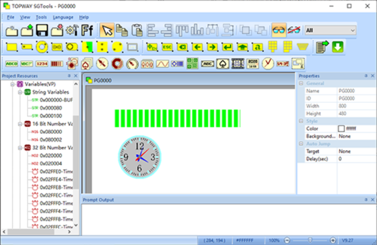
Graphical UI Editor, enables quick user interface construction, speeds up product’s time-to-market
Preloaded UI design in smart LCD, provides speedy showing and updating
Embedded display engine, reduces main board workload and over-all cost
Built-in Lue Script language engine, empowers rich and friendly user interface
RJ45 port, supports long-distant update and easy expansion
Unified body, improves EMC performance and increases reliability
Smart LCD module works with five basic items:
Page – container for one UI screen, it holds page elements
Element – functional display unit on a page. Such as Action, Character, Image etc.
-9 action type elements
-6 character type elements
-6 image type elements
-8 graphic type elements
Call Function – function that can be triggered by Page start, Touch Key or Virtual Touch Key press action
-14 keyboard functions
-20 operations
VP Variable – a RAM area for holding temporary value. It supports host access, on-screen keyboard input and value operations
Image Resource – images linked by elements or pages for displaying, including background images, icon and animated images
Topway’s UI Editor for smart LCD module provides a zero-coding way to construct human machine interface. User can drag & drop above basic items onto page and set up their properties according to need. You can find a short video demonstrating on how to build user interface in minutes with Smart LCD Module:
You can find more information about Smart LCD module by visiting the product page.
In most of our previous tutorials concerning operational amplifiers, only one input was applied to either the inverting or non-inverting op-amp’s input. This new article will deal with a configuration known as the summing amplifier which gives an output that is proportional to a weighted sum of the multiple inputs present.
The inputs can either be applied to the inverting or non-inverting branches which give two possible configurations that will be separately presented in the first and second sections. They are commonly referred as the inverting summing amplifier and non-inverting summing amplifier and we will see what are their differences and similarities.
In a third section, the dual configuration of the summing amplifier, the subtracting amplifier, is investigated.
Inverting summing amplifier
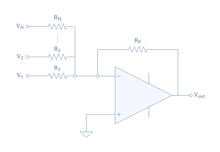
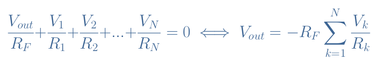
In Figure 1 we see the general circuit for an inverting summing amplifier:
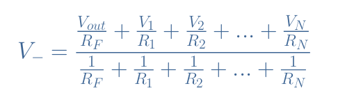
In this configuration, N inputs V1,V2,…,VN are applied to the inverting input of the op-amp through different resistor R1,R2,…,RN. The output Vout is feedbacked to the inverting branch through a resistor RF, the non-inverting input is grounded.
We can apply Millman’s theorem to V– in order to demonstrate the output relation of this circuit:
With the hypothesis of the ideal op-amp, i+=i–=0, and V+=V–=0, which leads to the output relation of the inverting summing amplifier:
eq 1: Output formula of the inverting summing amplifier
It is interesting to note that if we equalize all the input resistors with the feedback resistor, R1=R2=…=RN=RF, we obtain a simplified version for Equation 1:
eq 2: Simplified output formula with the resistor equality condition
In this case, the sum is not weighted anymore, and the inverting summing amplifier adds the inputs negatively as the output signal phase is in opposition with the inputs.
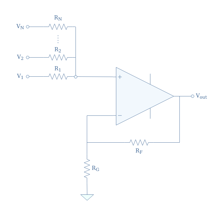
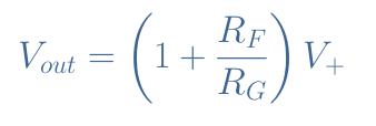
Non-inverting summing amplifier
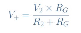
The non-inverting summing amplifier is a similar configuration to the inverting summing amplifier. However, the inputs here are applied to the non-inverting input while the inverting branch is connected to both the op-amp’s output through a feedback resistor RF and grounded through a resistor RG.
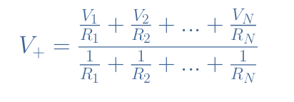
We can apply Millman’s theorem to V+ in order to demonstrate the output relation of this circuit:
Since the voltage gain Vout/Vin=Vout/V+ of a non-inverting configuration is given by 1+(RF/RG), we can conclude that the general relation for the non-inverting summing amplifier output is given by Equation 3:
eq 3: Output formula of the non-inverting summing amplifier
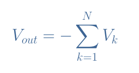
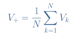
The expression of V+ can be extremely simplified if we pose R=R1=R2=…=RN, we get indeed:
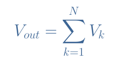
Moreover, we can also pose (1+RF/RG)=N in order to get a direct sum of the input voltages:
eq 4: Simplified output formula with the resistor equality condition
With these two conditions, we can see that the output voltage is a direct sum of the input signals as the sum is not weighted and no phase difference is present.
To conclude this section we can draw a little comparison between the inverting and non-inverting summing configurations. The advantage of the inverting configuration is that even in the general case, the output is simply expressed as a function of the different resistor and input values.
In a non-inverting configuration, the output is always in phase with the inputs which save the trouble to use an inverting buffer to rectify the signal. Moreover, the non-inverting configuration presents the property of having a much higher input impedance which is an advantage to properly inject the desired voltages from a source (microphone for example) to the inputs of the op-amp.
However, we have seen that the output voltage is a simple weighted sum only under a condition of equality between all the resistors in the circuit.
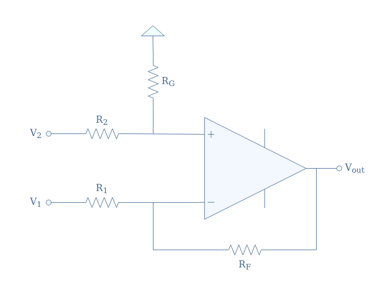
Subtracting amplifier
If the inputs are both applied to the inverting and non-inverting pins of an op-amp, a subtracting configuration is realized such as presented in Figure 3:
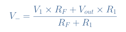
The voltage V+ can be expressed by a voltage divider formula:
The voltage V– is expressed thanks to Millman’s theorem:
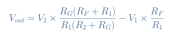
After reminding that V+=V–, a few steps of simplification lead to the general output expression of the subtracting amplifier:
eq 5: Output formula of the subtracting amplifier
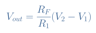
We can simply show by equalizing the two factors that if the condition RFR2=RGR1 is met, the output formula can be simplified to Equation 6:
eq 6: Simplified output formula for the subtracting amplifier
This condition can be achieved by equalizing all the resistances: R1=R2=RG=RF. In that case, since RF=R1, Equation 6 can be reduced to a direct subtraction Vout=V2-V1.
Applications
Audio mixer
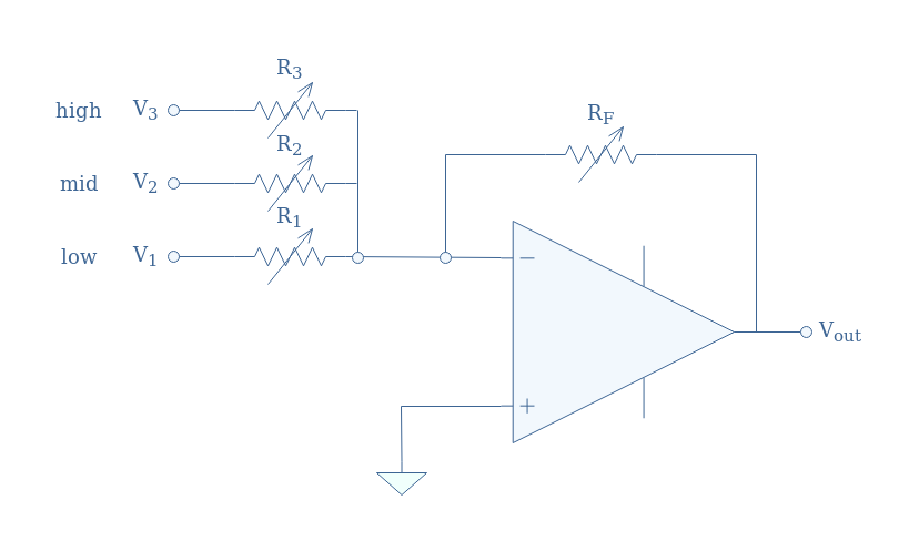
Consider an inverting summing amplifier with three inputs such as presented in Figure 4:
fig 4: Simple audio inverting summing amplifier
The resistors here are replaced by potentiometers in order for a user to directly control the output signal.
This type of configuration can be used in the audio domain where different pitches can be separately processed through an amplifier before being added together with possibly different prefactors.
Typically, the frequency ranges are given by:
low: 20 Hz to 500 Hz
mid: 500 Hz to 6 kHz
high: 6 kHz to 20 kHz
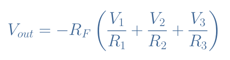
According to Equation 1, the output signal of this configuration is given by:
We can clearly identify that the potentiometer RF controls the global gain of the output, increasing or decreasing its value will simultaneously affect all the frequencies. On another hand, the potentiometers R1, R2, R3 only affect respectively the low, mid, and high pitches and they will enable the user to balance or unbalance certain frequencies.
We can note that if we want the output to be in phase with the different inputs, a simple inverting buffer can be used to rectify it.
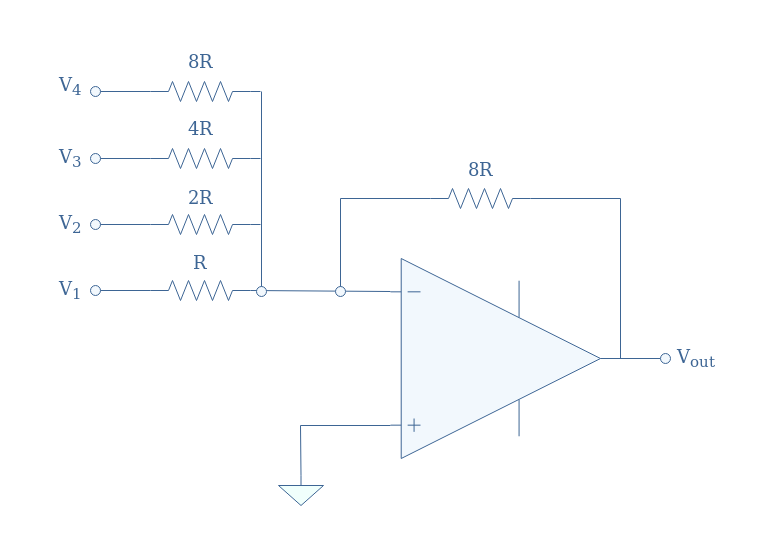
Digital to Analogue Converter (DAC)
A DAC is a summing amplifier based circuit that converts binary data (0 and 1) into an analog signal (a real number). An example of this circuit with four binary inputs known as a four-bit DAC and is presented in Figure 5:
fig 5: Four-bit DAC circuit representation
The values of the resistor are not chosen randomly, their values always need to double from the previous branch. This ensures a proper conversion from a binary number to a decimal number.
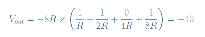
As an example, consider the binary four-bit input 1101 (V1=1 ; V2=1 ; V3=0 ; V4=1). According to Equation 1, the output is given by:
This validity of this result can be confirmed when we manually convert the same input to a decimal number: (1101)decimal=(1×23)+(1×22)+(0×21)+(1×20)=13.
In practice, the circuit shown in Figure 5 can only be implemented up to a certain number of bits depending on the precision of the resistors that must exactly double their value for each added bit. An alternative circuit known as the R-2R Ladder DAC is preferred for higher binary numbers.
Conclusion
A summing amplifier can either be based on an inverting or non-inverting configuration. Despite the high input impedance and in-phase output signal that the non-inverting summing amplifier can provide, the inverting summing amplifier is more common as it’s output is a simple weighted sum.
Indeed, the non-inverting summing output is a simple weighted or direct sum of the inputs only when a condition of equality between all the resistors in the circuit is met.
After presenting and detailing these two summing configurations, a third section has presented the subtracting amplifier which slightly differs from the summing amplifiers and is used to subtract two or more signals by applying them both on the inverting and non-inverting pins.
Finally, in the last section, we present the possible applications of the summing amplifiers. Indeed, an inverting summing amplifier can be used as an audio mixer in order to separately control each input importance, the inputs can, for example, be frequency ranges or different instruments outputs.
We also show that summing amplifiers can be used as a simple digital to analog converters when the resistance value for each added bit is doubled.
InPlay Technologies, headquartered in Shanghai, China, today launched the world’s smallest software-free programming Bluetooth beacon SoC, IN100, based on its NanoBeaconTM technology.
The product is a software-free programming SoC, which will greatly reduce the technical threshold. Any developer can easily build their own wireless applications without worrying about learning complex Bluetooth protocol stacks and embedded programming languages.
The package size of this SoC is as small as 2.0mm x 2.5mm, making it an ideal solution for the next generation of wireless beacon or wireless sensor applications.
IN100 integrates low-power Bluetooth 4.2 technology, supports LE broadcast and private protocol broadcast modes, and the format is compatible with mainstream iBeacon, Eddystone and WeChat Beacon. Developers only need to configure the pre-defined ID and broadcast parameters in the one-time programmable (OTP) memory of IN100. As long as the device is turned on, it will operate as a Bluetooth beacon and broadcast with the preset ID information .
IN100 also supports various types of sensor interfaces, including analog signals and single-bus digital pulse counting interfaces. Developers can easily connect IN100 to analog or digital sensors and configure sensor thresholds. Once the threshold is reached, they can wirelessly issue alarms or broadcast raw sensor data through its Bluetooth beacon working mode.
IN100 SoC is available in DFN8 (2.0mmx2.5mm) and QFN20 (3.0mmx3.0mm) packages. Samples will be available in the fourth quarter of 2020, and mass production is expected in the first quarter of 2021.
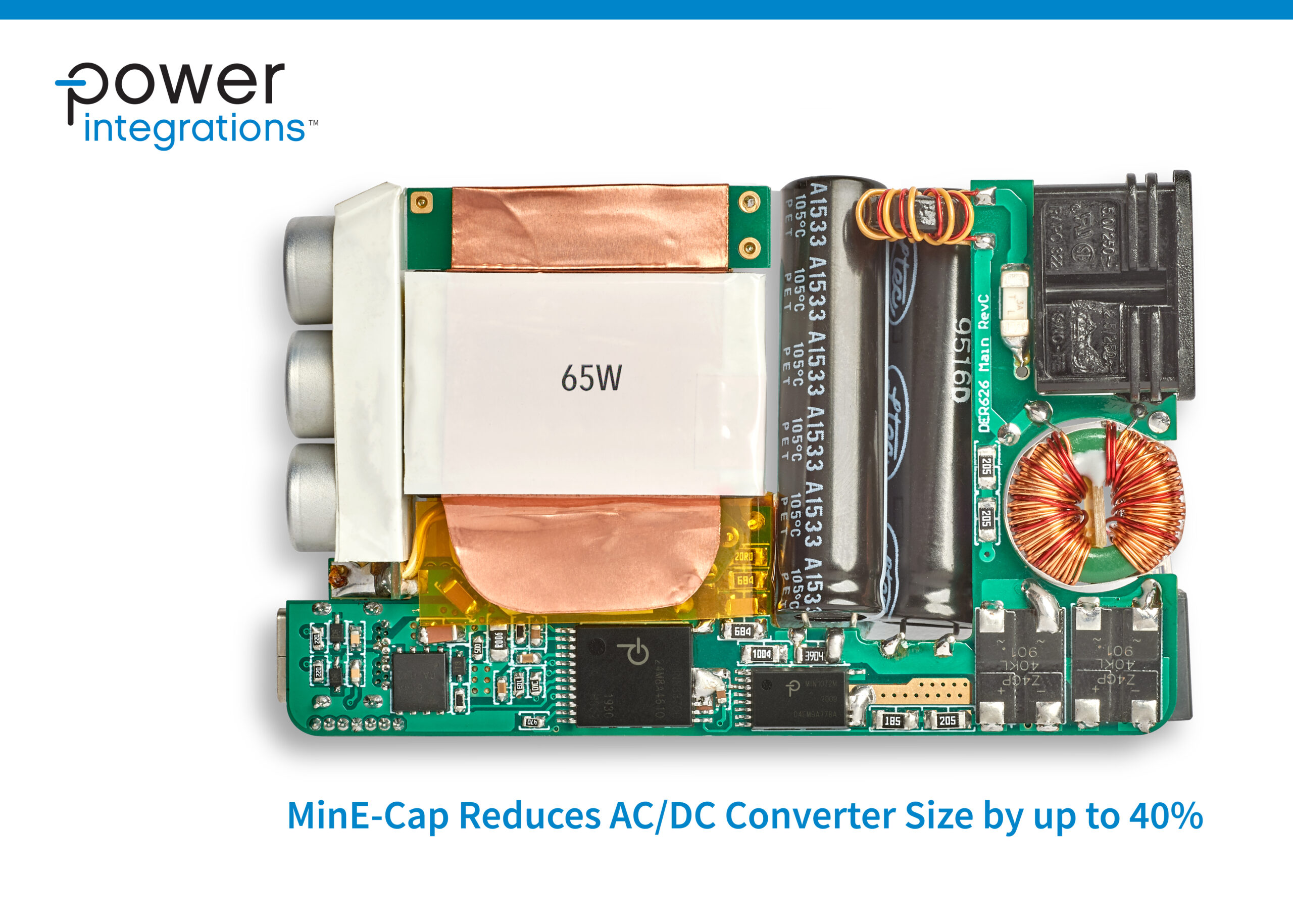
Power Integrations , the leader in high-voltage integrated circuits for energy-efficient power conversion, announced the MinE-CAP™ IC for high power density, universal input AC-DC converters. By halving the size of the high-voltage bulk electrolytic capacitors required in offline power supplies, this new type of IC enables a reduction in adapter size of up to 40%. The MinE-CAP device also dramatically reduces in-rush current making NTC thermistors unnecessary, increasing system efficiency and reducing heat dissipation.
Comments Power Integrations’ product marketing director, Chris Lee:
“The MinE-CAP will be a game-changer for compact chargers and adapters. Electrolytic capacitors are physically large, occupy a significant fraction of the internal volume and often constrain form factor options – particularly minimum thickness – of adapter designs. The MinE-CAP IC allows the designer to use predominantly low voltage rateding capacitors for a large portion of the energy storage, which shrinks the volume of those components linearly with voltage. USB PD has driven a major market push towards small 65 W chargers and many companies have concentrated on increasing switching frequency to reduce the size of the flyback transformer. MinE-CAP provides more volume saving than doubling the switching frequency, while actually increasing system efficiency.”
The MinE-CAP leverages the small size and low RDSon of PowiGaN™ gallium nitride transistors to actively and automatically connect and disconnect segments of the bulk capacitor network depending on AC line voltage conditions. Designers using MinE-CAP select the smallest high-line rated bulk capacitor required for high AC line voltages, and allocate most of the energy storage to lower voltage capacitors that are protected by the MinE-CAP until needed at low AC line. This approach dramatically shrinks the size of input bulk capacitors without compromising output ripple, operating efficiency, or requiring redesign of the transformer.
Conventional power conversion solutions reduce power supply size by increasing switching frequency to allow the use of a smaller transformer. The innovative MinE-CAP IC achieves just as significant overall power supply size reduction while using fewer components and avoiding the challenges of higher EMI and the increased transformer/clamp dissipation challenges associated with high-frequency designs. Applications include smart mobile chargers, appliances, power tools, lighting and automotive.
Said Bhaskar Thiagaragan, Director of Power Integrations India Ltd.:
“MinE-CAP ICs are excellent for all locations with wide ranging input voltages. In India we often design for voltages from 90 VAC to 350 VAC, with a generous surge de-rating above that. Engineers here often complain about the forest of expensive high-voltage capacitors required. MinE-CAP dramatically reduces the number of high-voltage storage components, and shields lower voltage capacitors from the wild mains voltage swings, substantially enhancing robustness while reducing system maintenance and product returns.
Housed in the miniature MinSOP-16A package, the new devices work seamlessly with Power Integrations’ InnoSwitch™ family of power supply ICs with minimal external components. MinE-CAP MIN1072M ICs are available immediately from PI offices and franchised distributors and are priced at $1.75 for 10 Ku. Two initial design example reports (DERs) pair the MinE-CAP IC with Power Integrations’ InnoSwitch3-Pro PowiGaN IC, INN3370C-H302. A 65 W USB PD 3.0 power supply with 3.3 V – 21 V PPS output for mobile phone / laptop chargers is described in DER-626, and DER-822 describes a 60 W USB PD 3.0 power supply for USB PD/PPS power adapters using INN3379C-H302.
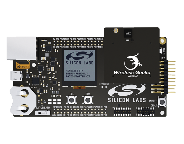
Silicon Labs’ BGM220 Explorer Kit is focused on rapid prototyping and concept creation of IoT applications. It is designed around the BGM220P module, based on the EFR32BG22 system-on-chip, which is an ideal device family for developing energy-friendly connected IoT applications.
The kit features a USB interface, an on-board SEGGER J-Link debugger, one user-LED and button, and support for hardware add-on boards via a mikroBus™ socket and a Qwiic® connector. The hardware add-on support allows developers to create and prototype applications using a virtually endless combination of off-the-shelf boards from mikroElektronika, Sparkfun, AdaFruit, and Seeed Studios.
As a maker, often we are faced with people who are afraid to dive into this world, mainly because they are scared to start their own projects and think the task of learning to code is a total abomination (it is not) or just want to do very simple stuff and do not feel like their small idea is worth the effort of learning. Either way, there is a new way to go about very simple projects, the Blokdots platform.
Now, to the obvious question: what is Blokdots? Simply put in their terms, it is “a simple to use software to build interactive hardware prototypes without writing a line of code”. Now, you may have seen the general principle before, where through a GUI you can configure your MCU with its initialization code (like on STM32CubeMX), the principle is not exactly the same here: in Blokdots, you get an even more simplistic (because you do not want to scare people off right away with PWM, GPIO and other technical terms), general language way of explaining what your prototype should do.
To easily interact with the app, you get a shield that plugs on top of your Arduino, that is meant to ease out the most technical details. When you open Blokdots, you get two windows: a “live view” window and the project on the right. On the live view, you configure the slots you plug components into (such as LCD’s buttons, LED’s, among others). If you are overwhelmed by the number of slots, they provide you with a wizard that will interactively show you where you connect the components. After configuring the connected components on the left, you can go the project window to add logic to them. From there, you select a card that tells you what the component should do. Once clicking on a card, you are presented with regular language and not the programming you are used to, making it easier for non-programmers to dive into this sort of projects. When you are done, you can add another card (as many as you like) or save and run it on the Arduino board. Quite easy as that!
Lastly, let us talk about what you need to get started. The Blokdots app, which is only available for Mac, which is the most saddening part, since a lot of people that may be interested in this sort of product use Windows. Then, you need the components, which follow the widely available Grove system. There are a lot of them to choose from, like LCD’s, motors and some sensors, so you are not limited there. Overall, aside from the development OS limitation, we think this can be very useful for people who are not very confortable with programming and just want to do something simple from time to time, because if you want to do more (and you can do some cool things there), you should program, it’s fun.
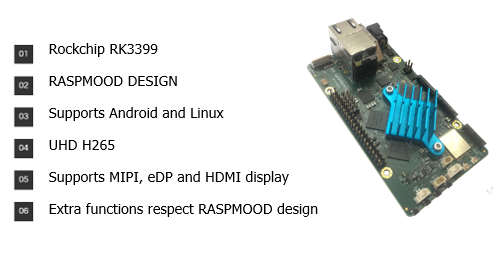
The SBCs M-line was created for those advanced multimedia applications, where the computing power and the presence of specific HW accelerators, are needed as much as the advanced connectivity to various kinds of displays while maintaining the classic low-level industrial connectivity.
A new generation high performance industrial SBC
The latest product of the M-Line is Novasom M9 which joins the well-established M7 and M7Plus. This SBC is based on the prestige Rockchip 3399. This CPU offers the new Cortex A72’s performance and the multicore Quad A53 used to speed-up parallelism and lower consumption when needed, with one of the strongest GPU available on the market: the Mali-T860MP4. This board has been minded to offer the latest and strongest video input-output capability, while minding to our RASPMOOD approach with USB extender and low level GPIO to assure the compatibility with the famous community board’s started application. As any Industrial Novasom’s SBC, the unit is equipped with our famous protected power supply, minded as industrial in terms of emission, susceptibility, mission profile and assisted by our technical support that will assure the success of your application. This is an Android-graphics oriented minded SBC, offering a superior fluidity experience for any tablet like or digital signage application.
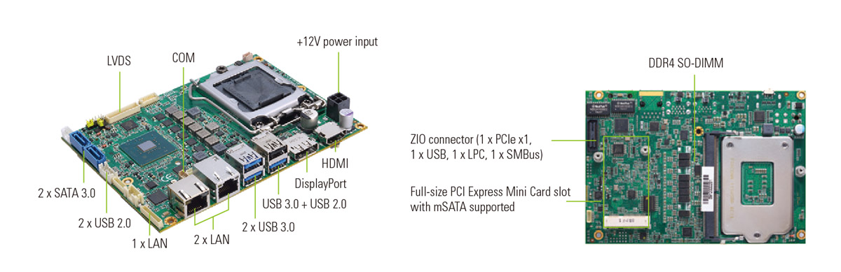
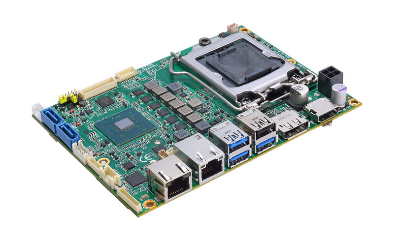
Axiomtek – a world-renowned leader relentlessly devoted in the research, development and manufacture of series of innovative and reliable industrial computer products of high efficiency – is pleased to introduce the CAPA520, its new 3.5” embedded board featuring the LGA1151 socket 9th/8th generation Intel® Core™ i7/i5/i3 and Intel® Celeron® processors (code name: Coffee Lake) with the Intel® H310 chipset (Q370 optional). The industrial-grade CAPA520 with a size of 146 mm x 104 mm features triple-display capability through HDMI, LVDS and DisplayPort interfaces, enabling multi-display applications in a limited space. This powerful embedded SBC is optimized for various industrial IoT-related applications in the embedded market, such as industrial control, machine vision, self-service terminal, digital signage, and medical imaging.
“With rich I/O connectivity and great expansions, the highly integrated CAPA520 was designed to shorten the time to market and reduce development costs. It delivers powerful 3D and 4K graphics through the integrated Intel® UHD Graphics 630. Moreover, it can operate in a wide temperature range from -20°C to 60°C,”
said Leo Chen, a product manager of the Product Planning Division at Axiomtek.
“To ensure reliable and stable operation, this 3.5-inch embedded SBC supports the Intel® AMT 12 for easy remote management and monitoring and has hardware monitoring function to monitor CPU/system temperature, voltage and fan speed.”
The CAPA520 supports one 260-pin DDR4-2666 SO-DIMM for up to 16GB of system memory. To meet customer varied needs, the Intel® Core-based embedded board is equipped with one PCI Express Mini Card slot with mSATA support and an exclusive Axiomtek ZIO connector with USB, PCIe, LPC and SMBus expansion buses. It has one RS-232/422/485 port, three Gigabit Ethernet ports with Intel® i211AT and intel® i219LM controllers, three USB 3.0 ports, three USB 2.0 ports, one HDMI port, one LVDS port, one DisplayPort port, HD audio and 8-channel DIO port. The outstanding CAPA520 has a +12V DC power supply input with AT auto power on. It supports Windows® 10 and Linux.
The CAPA520 is now available for purchase. For more product information or customization services, please visit our global website at www.axiomtek.com or contact one of our sales representatives at info@axiomtek.com.tw.

 Laird has introduced Sentrius™ MG100 micro-gateway with LTE-M/NB-IoT and Bluetooth 5