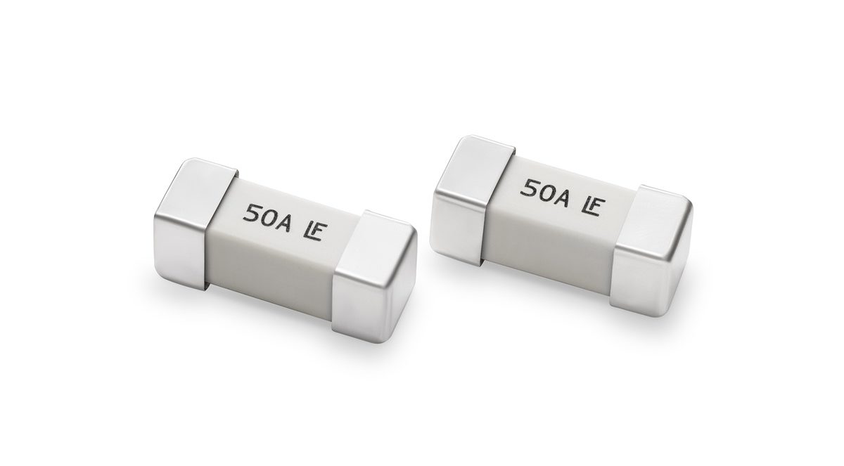
Bel Fuse and premier global manufacturer of circuit protection devices, announces their 0ZT Series of high temperature SMD resettable PPTC fuses for automotive, ethernet, and other applications which require a high operating temperature range of -40°C to 125°C. The 0ZT Series include five different chip sizes: 0ZTF (2920), 0ZTG (1812), 0ZTH (1210), 0ZTJ (1206) and 0ZTK (0805).
Bel’s 0ZT Series are small surface mountable, solid-state resettable fuses which feature a faster time to trip and lower resistance than standard SMD devices. All are AEC-200 compliant and ideal for automotive applications, such as electronic systems control and monitoring, infotainment, climate control, and lighting and ADAS (Advanced Driver Assistance), as well as security-focused applications.
The 0ZT Series fuses are RoHS 2 compliant, halogen-free and lead-free. Also, they are packaged in tape and reel for the auto-insert SMD process and meet the Bel automotive qualification, which is based on the AEC-Q200 test plan. The 0ZT Series is in stock with Digi-Key, Mouser, and Arrow in 2,000, 3,000, or 4,000 pieces in tape and reel. Product samples are also available upon request. Detailed information on the 0ZT Series fuses can be found here.
Designers of automotive chargers now have the industry’s smallest and lowest-cost solution with the MAX25430 100W USB Power Delivery (PD) buck-boost controller and protector from Maxim Integrated Products. As the industry’s most integrated solution, the MAX25430 can reduce design size up to 40 percent compared to competitive solutions and offer the industry’s lowest cost for increasing the number of USB PD ports in vehicles
Automotive multimedia hubs, including rear-seat entertainment modules and head units, are all expanding in capability as more USB PD chargers are integrated into passenger vehicle cabins. However, there are size, cost, and power constraints – and the MAX25430 addresses all of these.
The MAX25430 integrates a USB Type C Port Controller (TCPC) power regulator, VCONN cable power supply, buck-boost, and protection, thereby eliminating heat-sink requirements and metal box enclosures to further slash design size by 40 percent compared to competitive multi-IC solutions. In addition, bill-of-materials (BOM) costs are also reduced by 25 percent compared to competitive solutions. The MAX25430 runs 20-degrees (Celsius) cooler at full power compared to competitive automotive USB PD solutions. It needs only one microcontroller (MCU) regardless of the number of ports, while competitors require additional MCUs per port.
For a complete solution, Maxim Integrated also offers the MAX25410 automotive USB PD port protector and the MAX25431 automotive 40V H-bridge buck-boost controller, meeting a wide array of USB charger design needs.
Key Advantages
Smallest Size: Integrates TCPC power regulator, VCONN power cable supply, buck-boost, and protection to reduce solution size up to 40 percent
Lowest Cost: Eliminates heat sinks, enclosure boxes, and multiple MCUs to yield 25 percent cost savings
Power Performance: Robust performance in harsh automotive environments while running 20 degrees cooler than the closest competitor
Availability and Pricing
For details about Maxim Integrated’s automotive USB PD solutions, visit http://bit.ly/Automotive_USBPD. The MAX25430BATLG/V+T is available at Maxim Integrated’s website for $4.17 (1000-up, FOB USA), and the MAX25430AEVKIT# evaluation kit is available for $299.
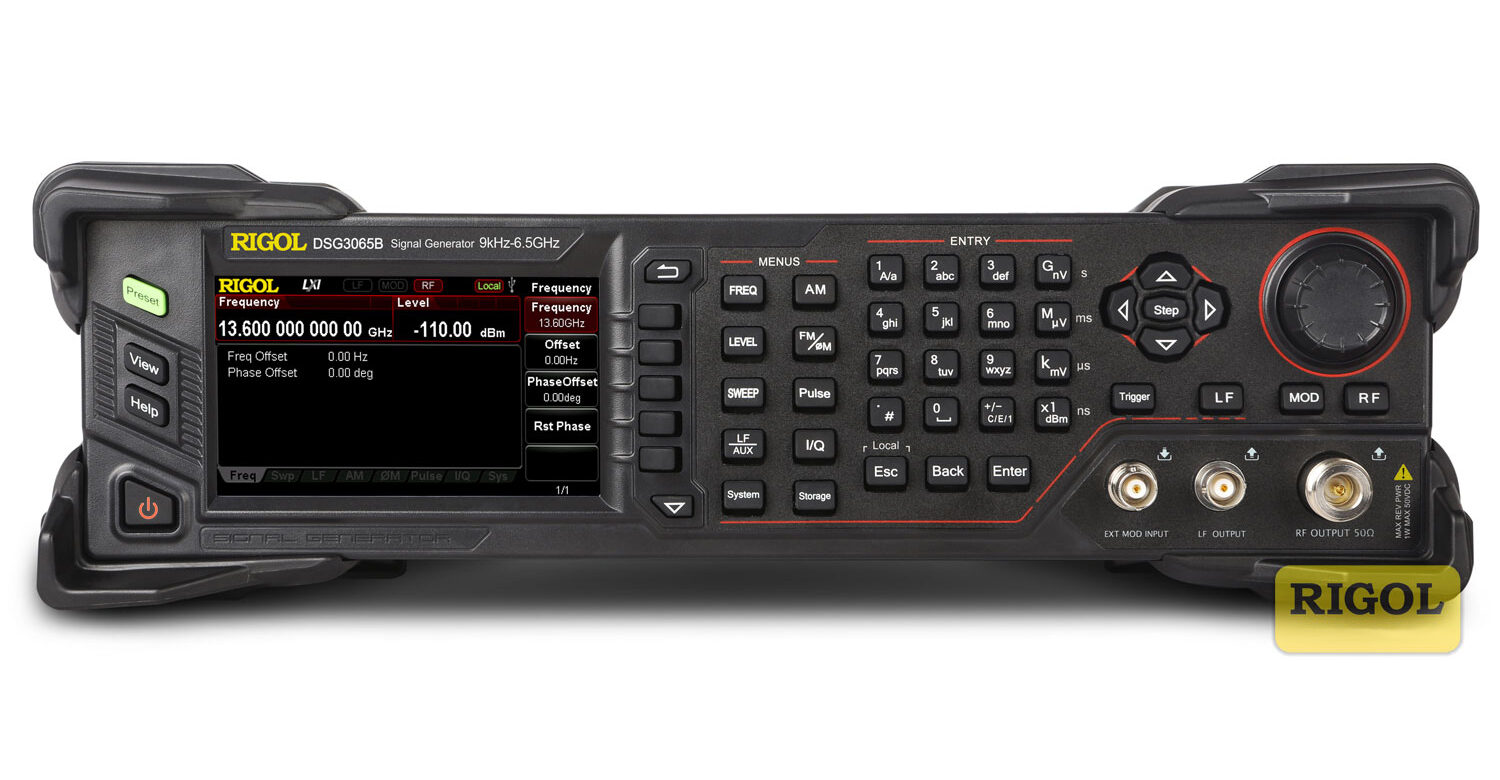
The DSG3000B RF Signal Generator series simplifies high power setup since an external amplifier is not needed. Engineers can generate more complex signals without additional hardware using the modulation schemes supplied in the DSG3000B with both internal and external IQ modulation capabilities.
Saelig Company, Inc. has introduced the Rigol DSG3000B RF Signal Generator series, improving on the previous DSG3000 series, covering a frequency range of 9kHz to 6.5GHz or 13.6GHz and including IQ modulation variants. These HF signal sources have an amplitude accuracy of <0.5dB (typical) and a phase noise of less than -116dBc/Hz @ 20kHz. The output is specified from -120dBm to + 20dBm and can be set for a frequency range from 200MHz to 3.6GHz up to + 27dBm, or from 100kHz to 6.5GHz to -130dBm. The <2ppm standard frequency stability of the internal reference clock can be enhanced with an optional 5ppb clock. Standard modulations of AM/FM /PhaseM up to 3.6 GHz are provided with a frequency resolution of 0.01Hz. All modulations can be controlled by an internal or external source. The 4.3” TFT LCD with menu keys and logical front panel button/wheel control make for an easy to use instrument. USB and LAN are available as standard remote control interfaces, as is support for SCPI control commands.
The functionality of the signal generators can be expanded with three options: an oven-controlled quartz clock OCXO-B08 improves the temperature stability of the internal reference frequency from <2ppm to 5ppb. Also, pulse train generation DSG3000B-PUG and pulse modulation DSG3000B-PUM are available (usable up to 3.6GHz).
High frequency range: 6.5GHz/13.6GHz
Excellent Amplitude accuracy: <0.5dB (typical)
Output amplitude range: -130dBm to +27dBm
High signal purity, phase noise: <-116dBc/Hz@20kHz (typical)
Standard 1ppm internal clock; optional 5ppb high stable clock
Standard AM/FM/PhaseM analog modulation
Supports pulse modulation; on/off ratio up to 70dB; user-defined pulse train generation
I/Q modulation and I/Q baseband output
All modulations support internal and external modulation modes
Standard 2U height design to save rack space; rack mount kit is available
Supports USB/LAN/GPIB remote control; SCPI command set
Wear-free electronic attenuator design
Made by Rigol Technologies Inc., a leading manufacturer of precision electronic instrumentation for test and measurement, the DSG3000B RF Signal Generator series is available now from Saelig Company, Inc., their USA technical distributor.
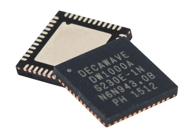
Recently, Qorvo, a leader when it comes to providing us with innovative RF solutions for our communication needs, acquired Decawave, a pioneer in UWB (Ultra Wide Band) technology dedicated to mobile, automotive and IoT applications. But what does this mean for us, engineers? Well, it means more options in the market, which is always a “yes, please!”.
More in depth, it means a new lineup of products by Qorvo, making use of Decawave’s UWB technology, more concretely, on the new DW1000 UWB transceiver IC, the world’s first transceiver based on UWB techniques enclosed in a single chip. But what makes the DW1000 so special? Let’s see: it enables you to develop cost-conservative RTLS (Real-Time Locating System) solutions with extremely precise indoor and outdoor positioning, of 10 cm! It provides a new approach to real-time location and indoor positioning systems, location-based services, wireless sensor networks and other IoT applications by providing accurate location awareness and communication. It is compliant with the IEEE802.15.4-2011 standard, capable of up to 6.8 Mbps communication speeds. Some other characteristics described by Decawave about this module are:
Centimeter accuracy that is 100 times better than WiFi and Bluetooth
High immunity to multipath and interference, which allows reliable communications in high fading environments
Latency 50 times faster than GPS
Affordable: low power, low cost and low processing, allowing for operation on batteries for long periods
High data rate (6.8 Mbps)
Up to 290 meters range
Small package size and footprint, allowing for its inclusion in cost-effective WSN and RTLS solutions
Regarding applications, you get a lot of uses for this new technology, the “where” to apply this product is certainly not a problem as you can, for instance, make mobile accessories with it that enable secure payments, keyless entry, enhance navigation and help find your device, deliver real-time performance analysis in sports, in drones for flight control, in smart homes to control the connected devices based on the location of the persons, in factories to improve operational efficiencies and personnel safety, among other things. Overall, the areas of interest are smart homes, smart cities, security, health, fitness, connectivity between people, industrial internet, mobile accessories and automotive.
About the options you get when using this UWB technology, you can acquire the DW1000 transceiver IC itself or modules and evaluation kits. You can even use this module easily with the Arduino platform, due to a compatible shield. Regarding the pricing, it can range from $23 for the DW1000 module to $255.75 for a full on development kit, which is neat for the set of features this technology enables you to do. Overall, we think there is a lot of room for exploration, specially because of how recent it is and the potential it carries.
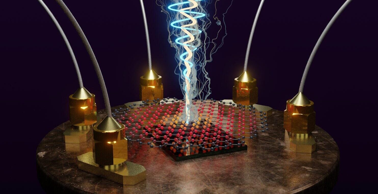
A new microwave radiation sensor with the sensitivity of up to 1 single photon, has been developed by research funded by the US Army and various pristine universities. This sensor is a microwave bolometer that can improve thermal imaging, radio communications, and RADAR by 100,000 times. The Army, in part, funded the work to fabricate this bolometer by taking advantage of the wonderful thermal response of graphene to microwave radiation. Graphene is this single layer (monolayer) of carbon atoms, tightly bound in a hexagonal honeycomb pattern. It is the thinnest, lightest, strongest, and most conductive material known to mankind.
The microwave bolometer developed under this project is so sensitive that it is capable of detecting a single microwave photon, which is the smallest amount of energy in nature,
said Dr. Joe Qiu, program manager for solid-state electronics and electromagnetics, Army Research Office.
This technology will potentially enable new capabilities for applications such as quantum sensing and radar, and ensure the US Army maintains spectral dominance in the foreseeable future.
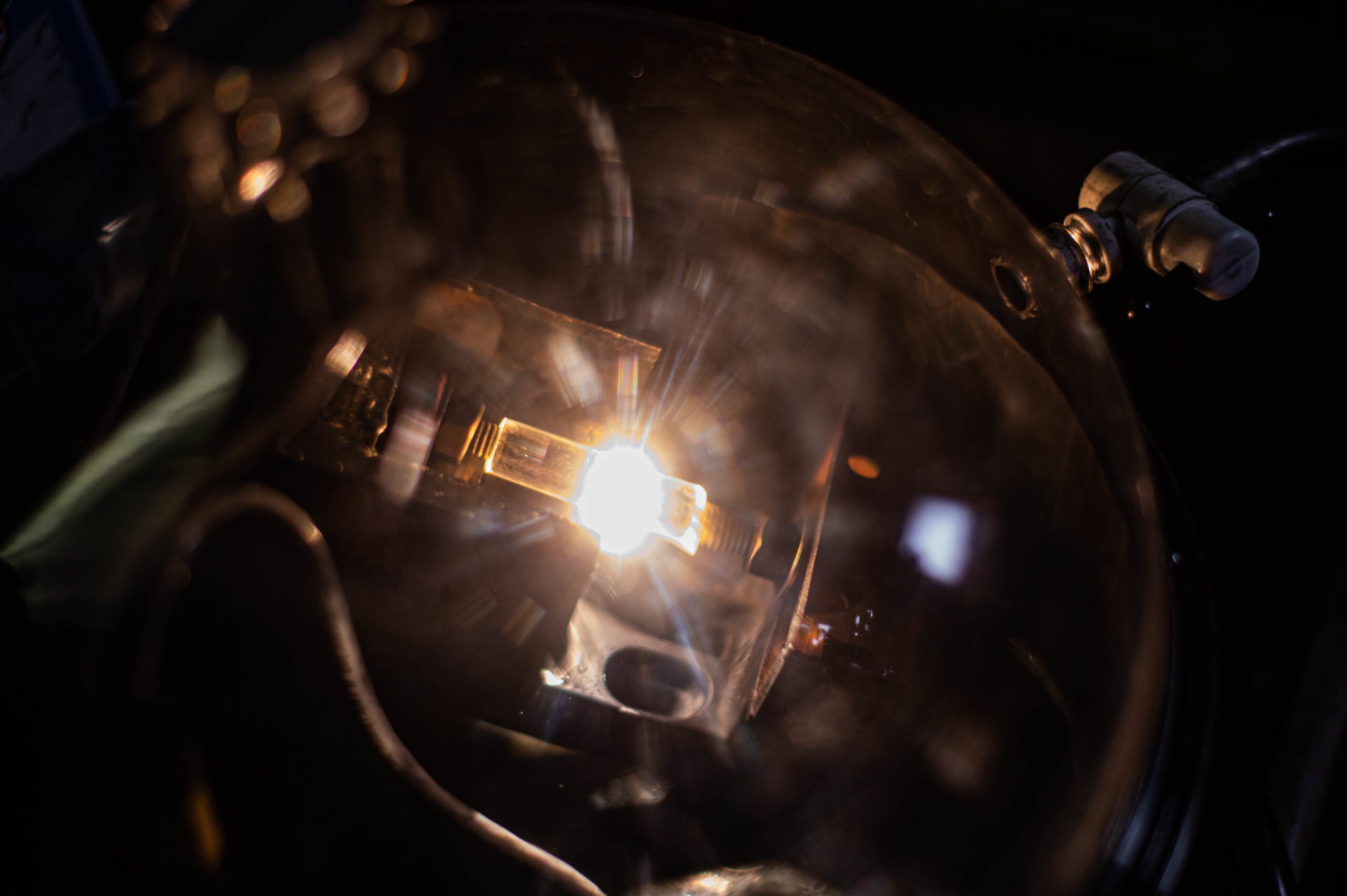
Single Layer Graphene getting heated by Microwave
As in every bolometer, this new graphene microwave bolometer sensor detects electromagnetic radiation and its energy by measuring the temperature rise when the incoming photons are absorbed into the sensor. Mainly the use of graphene and superconducting Josephson junction is the key to the huge leap in sensitivity for this new sensor. To measure the temperature rise while maintaining a high microwave radiation coupling into the graphene through the antenna is one of its key principle of work. This coupling efficiency is very essential for the high sensitivity detection of every single microwave photon.
The main reason for using graphene is the electrons in graphene are in a very special band structure where the valence and conduction bands meet at only one point, known as Dirac point. The density of different states vanishes there so that when the electrons receive the photon energy, the temperature rise is high while the heat leakage is small. Thus, making it the perfect sensing material for microwaves.
This research has also found a new way to improve the performance of RADAR, night vision, LIDAR (Light Detection and Ranging), and various electromagnetic communication devices. The findings can also be valuable in the fields of quantum information science, thermal imaging as well as the search of dark matter. As of now, creating high-quality graphene cheaply and efficiently was a huge challenge. But, as we saw with the discovery of the flash-graphene-making process, manufacturing challenges can be omitted in near future.
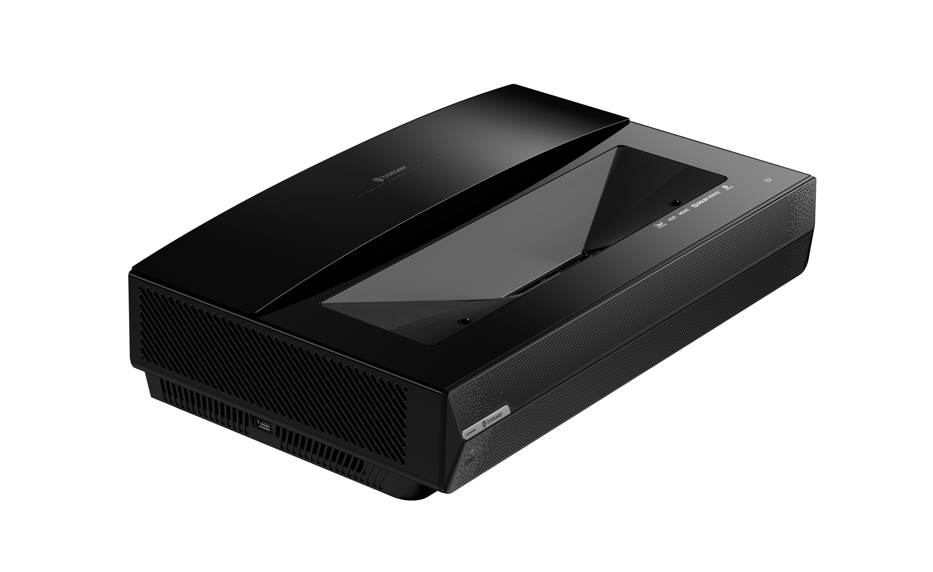
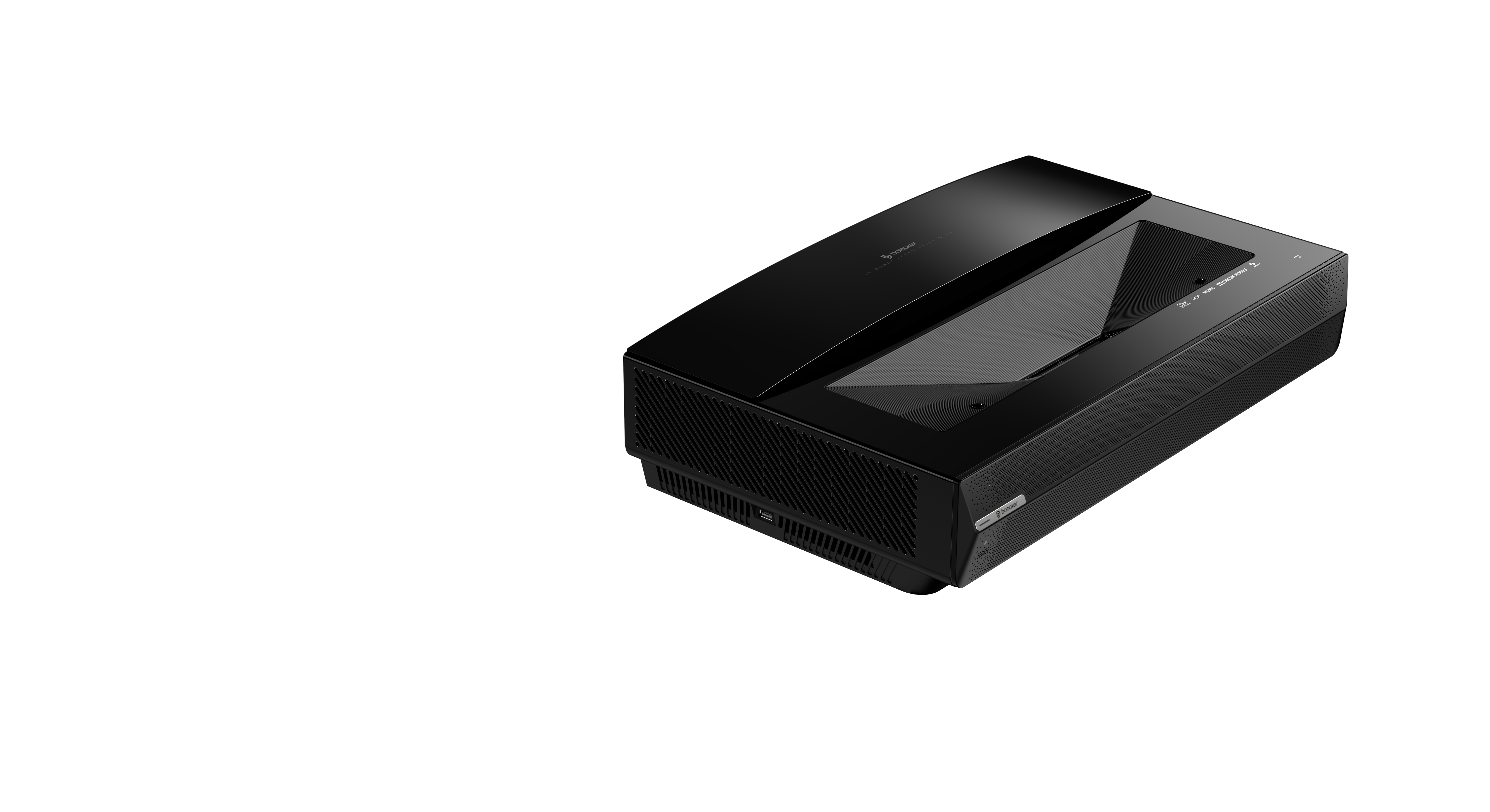
Bomaker, a leading manufacturer of projection and audio products, will unveil a brand new 4K ultra short throw laser TV-Polaris 4K on Kickstarter soon.
Bomaker Polaris 4KLaser TV is an ultra-short throw laser projector adopting the tricolor laser technology which delivers stunning imagery and an immersive viewing experience highlighted by 2500 ANSI lumens of brightness, 107% BT.2020 wide color gamut, and HDR 10 support.
Adopted the latest tri-color laser light source technology, Polaris can emit at the same time red, green, and blue light. A wider range of colors can be obtained by mixing different proportions of red, green and blue light, which can fully cover the BT. 2020 and express a much more vivid picture with virtually no color loss compared to conventional projectors (DLP, Laser and Dual Laser).
With an incredible 8.3 million pixels (3840 x 2160), and equipped with a high-end Ricoh lens, the Polaris 4K laser TV delivers a crisper picture, more realistic colors, and greater details using four times more pixels than standard HD. You’ll wonder how you watched movies before the Polaris.
It is worth mentioning that Polaris 4K laser TV has the ability to sense the distance of the object, and automatically reduce the luminance within 0.4-1 meter and provide a more comfortable watching experience.
Featuring MEMC motion compensation technology:
Polaris 4K makes it possible to artificially create additional frames for movies and videos. This means that a movie that comes at 30fps can be viewed at 60 or even 120fps. No matter how fast-moving the picture is, it makes the viewing experience more seamless, smoother, and more attractive.
Should you be interested, the Polaris 4K Laser TV will launch soon on Kickstarter with only $2299. Sign up now to enjoy the super early bird discount at $1999 (31% off the $2899 MSRP) for the first 50 backers only.
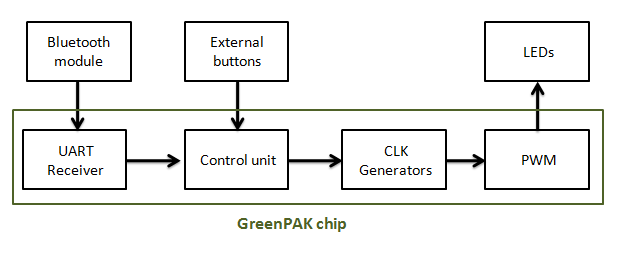
This article describes how to build a smart digital dimmer. A dimmer is a common light switch that is used in houses, hotels and many other buildings. Older versions of dimmer switches were manual, and would typically incorporate a rotary switch (potentiometer) or buttons to control the light level. This article describes how to build a digital dimmer that has two ways of controlling light intensity; a smartphone and physical buttons. The two modes can work seamlessly together so that the user can increase or decrease luminosity from both a button and smart phone. The project is implemented using a SLG46620V CMIC, HC-06 Bluetooth module, push buttons and LEDs.
We are going to use the SLG46620V CMIC as it helps minimize discrete project components. GreenPAK IC’s are small and have multiuse components, which allows a designer to decrease components and to add new features. Additionally, the project cost is subsequently reduced.
The SLG46620V also contains a SPI connection interface, PWM blocks, FSM and a lot of useful additional blocks in one tiny chip. These components allow a user to build a practical smart dimmer which can be controlled via a Bluetooth device or wall buttons, support extended-time dimming, and the addition of selectable features without using a microcontroller or expensive components.
Project features:
Two methods of control; mobile app and real buttons.
Smooth on-off transition for the light. This is healthier for a consumer’s eyes. It also gives a more luxurious feeling, which is appealing to hotels and other service industries.
Sleep mode feature. This will be an added value for this application. When the user activates this mode, light brightness decreases gradually in 10 minutes. This helps people who suffer from insomnia. It is also useful for kid’s bedrooms and retail shops (closing time).
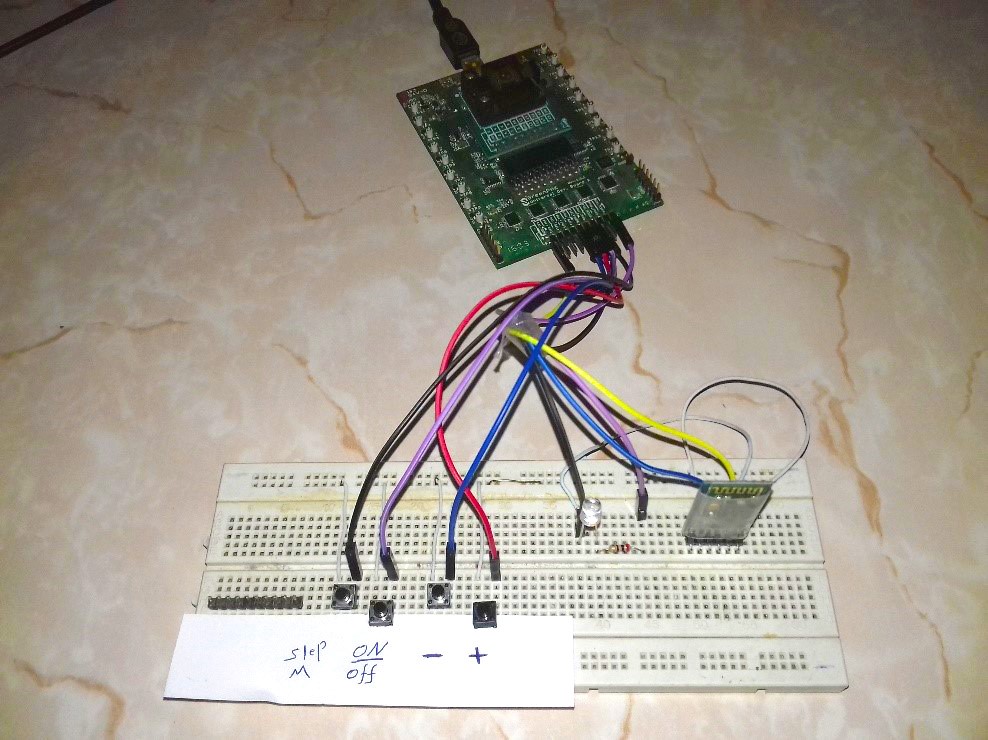
Project Interface
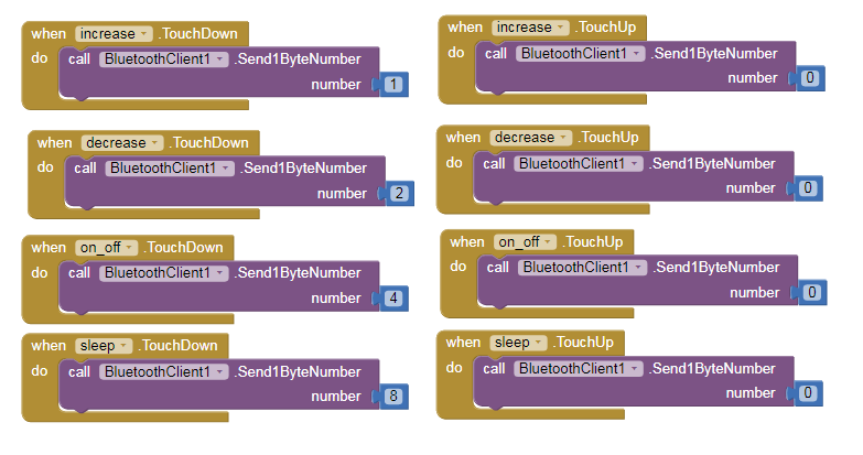
The project interface has four push buttons, which are used as GreenPAK inputs:
ON\OFF: turn the light ON\OFF (soft-start\stop).
UP: increase light level.
Down: decrease light level.
Sleep Mode: by activating sleep mode, light brightness decreases gradually over a period of 10 minutes. This gives the user time before sleeping and guarantees that the light will not stay ON all night.
The system will output a PWM signal, which will be passed to an external LED and sleep mode LED indicator.
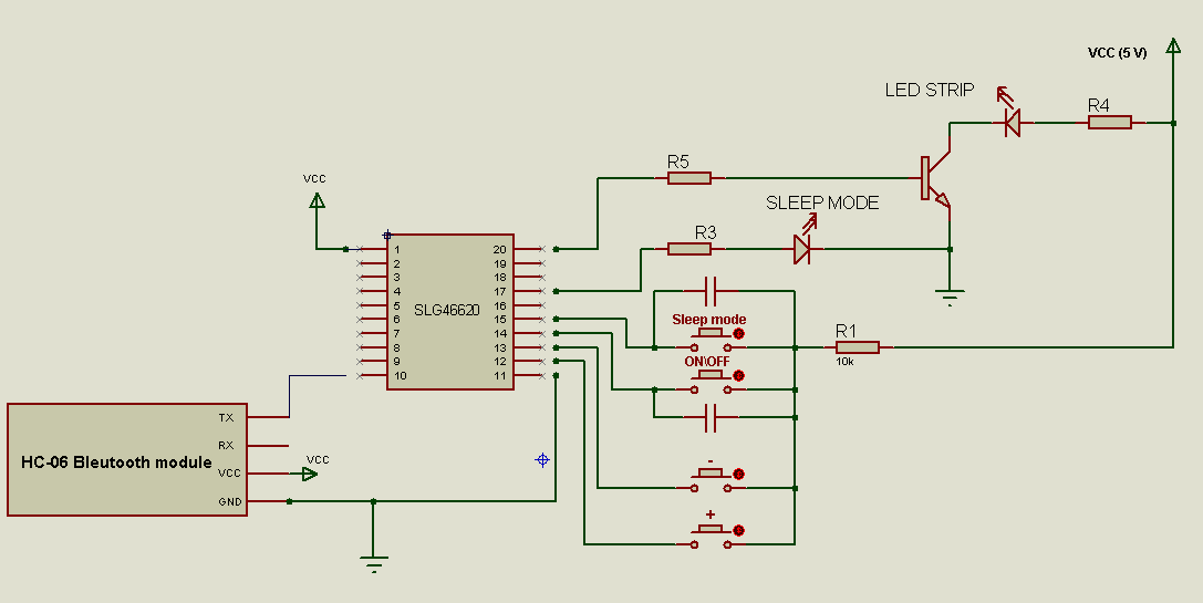
Figure 1: Dimmer Block Diagram
The GreenPAK design is comprised of 4 main blocks. The first is a UART receiver, which receives data from the Bluetooth module, extracts orders, and sends them to a control unit. The second block is a control unit, which receives orders coming from the UART receiver or from the external buttons. The control unit decides the required action (Turn ON/OFF, Increase, decrease, enable sleep mode). This unit is implemented using LUTs.
The third block supplies the CLK generators. In this project, a FSM counter is used to control the PWM. The FSM’s value will change (up, down) according to the orders given by 3 frequencies (high, medium, and low). In this section the three frequencies will be generated and the required CLK passes to FSM according to the required order; In turning on/off operation, high frequency passes to FSM to soft start/stop. During dimming, the medium frequency passes. The low frequency passes in sleep mode to reduce the FSM value more slowly. Then, light brightness decreases slowly too. The fourth block is the PWM unit, which generates pulses to external LEDs.
GreenPAK Design
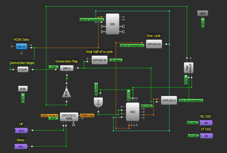
The best way to build a dimmer using GreenPAK is by using the 8-bit FSM and a PWM. In the SLG46620, FSM1 contains 8 bits and can be used with PWM1 and PWM2. The Bluetooth module must be connected, which means the SPI parallel output must be used. The SPI parallel output bits 0 through 7 connections are muxed with DCMP1, DMCP2, and LF OSC CLK, OUT1, OUT0 OSC outputs. PWM0 obtains its output from FSM0 (16 bits). FSM0 does not stop at 255; it increases up to 16383. To limit the counter value at 8 bits another FSM is added; FSM1 is used as a pointer to know when the counter reaches 0 or 255. FSM0 was used to generate the PWM pulse. As the two FSM’s values must be changed at the same time to have the same value, the design becomes a bit complex where in both FSMs have a predefined, limited, selectable CLK. CNT1 and CNT3 are used as mediators to pass the CLK to both FSMs.
First, we need to set up the HC06 Bluetooth module. The HC06 uses the UART protocol for communication. UART stands for Universal Asynchronous Receiver / Transmitter. UART can convert data back and forth between parallel and serial formats. It includes a serial to parallel receiver and a parallel to serial converter which are both clocked separately. The data received in the HC06 will be transmitted to our GreenPAK device. The idle state for Pin 10 is HIGH. Every character sent begins with a logic LOW start bit, followed by a configurable number of data bits, and one or more logic HIGH stop bits.
The HC06 sends 1 START bit, 8 data bits, and one STOP bit. Its default baud rate is 9600. We will send the data byte from the HC06 to the GreenPAK SLG46620V’s SPI block.
Since the Dialog SPI block does not have START or STOP bit control, those bits are instead used to enable and disable the SPI clock signal (SCLK). When Pin 10 goes LOW, the IC has received a START bit, so we use the PDLY falling edge detector to identify the start of communication. That falling edge detector clocks DFF0, which enables the SCLK signal to clock the SPI block.
Our baud rate is 9600 bits per second, so our SCLK period needs to be 1/9600 = 104 µs. Therefore, we set the OSC frequency to 2 MHz and used CNT0 as a frequency divider.
2 MHz-1 = 0.5 µs

(104 µs / 0.5 µs) - 1 = 207
Therefore, we want the CNT0 counter value to be 207. To ensure that data is not missed, a half clock cycle delay on the SPI clock is added so that the SPI block is being clocked at the proper time. This is accomplished by using CNT6, 2-bit LUT1, and the OSC block’s External Clock. The output of CNT6 does not go high until 52 µs after DFF0 is clocked, which is exactly half of our SCLK period of 104 µs. When it goes high, the 2-bit LUT1 AND gate allows the 2 MHz OSC signal to pass into the EXT. CLK0 input, whose output is connected to CNT0.
Figure 2: UART Receiver
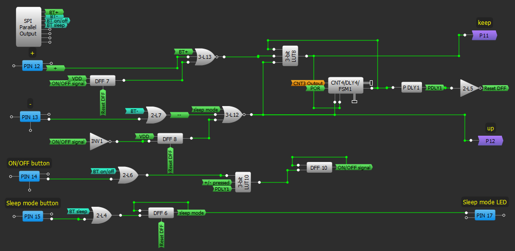
Control Unit
In this section, commands will be executed according to the received byte from the UART receiver, or according to the signals from the external buttons. Pins 12, 13, 14, 15 are initialized as inputs and are connected to external buttons.
Each pin is internally connected to an OR gate input, while the second input of the gate is connected with the corresponding signal that coming from the smartphone via Bluetooth which is going to appear on SPI Parallel output.
DFF6 is used to activate sleep mode where its output changes to high with the rising edge coming from 2-bit LUT4, while DFF10 is used to maintain the lighting status, and its output changes from low to high and vice versa with every rising edge coming from 3-bit LUT10 output.
FSM1 is an 8-bit counter; it gives a high pulse on its output when its value reaches to 0 or 255. Consequently, it’s used to prevent FSM0 (16-bit) from exceeding the value 255, as its output resets DFFs and it changes DFF10 status from on to off and vice versa if the lighting is controlled by the buttons +, – and the maximum/minimum level has been reached.
The signals connected to FSM1 inputs keep, up will reach FSM0 through P11 and P12 to synchronize and keep the same value on both counters.
Figure 3: Control Unit Design
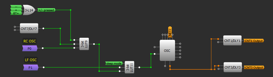
CLK Generators and Multiplexer
In this section, three frequencies will be generated, but only one will clock the FSMs at any one time. The first frequency is RC OSC, which is fetched from the matrix 0 through P0. The second frequency is LF OSC which is also fetched from the matrix 0 through P1; the third frequency is the CNT7 output.
3-bit LUT9 and 3-bit LUT11 allow one frequency to pass, according to the 3-bit LUT14 output. After that, the chosen clock transmits to FSM0 and FSM1 through CNT1 and CNT3.
Figure 4: Clock Generator Design
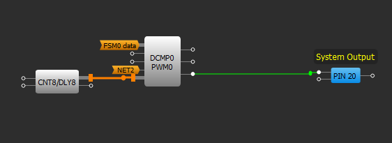
PWM
Finally, FSM0 value transforms to PWM signal to appear through pin 20 which is initialized as an output and it is connected to the external LEDs.
Figure 5: PWM Block
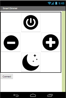
Android app
The Android app has a virtual control interface similar to the real interface. It has five buttons; ON\OFF, UP, DOWN, Sleep mode, and Connect. This Android Application will be able to convert button presses into a command and will send the commands to the Bluetooth module to be carried out.
This app was made with MIT App Inventor, which doesn’t require any programming experience. The App Inventor lets the developer create an application for Android OS devices using a web browser by connecting programming blocks. You can import our App into the MIT App Inventor by clicking on Projects -> Import project (.aia) from my computer, and selecting the .aia file included with this folder.
To create the Android Application a new project must be started. Five buttons are required: one is a list picker for Bluetooth devices, and the others are the control buttons. We need to add a Bluetooth client as well. Figure 6 is a screen capture of our Android Application’s user interface.
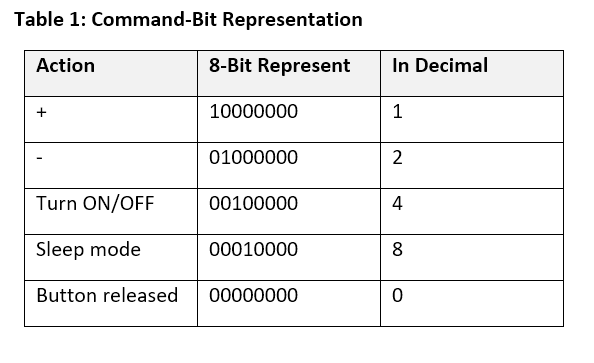
After we add the buttons, we are going to assign software function for each button. We are going to use 4 bits to represent the status of the buttons. One bit for each button, therefore, when you press the button, a specific number will be sent via Bluetooth to the physical circuit.
This article describes a smart dimmer that can be controlled in two ways; an Android app and real buttons. Four separate blocks are outlined within the GreenPAK SLG46620V which control the process flow for increasing or decreasing the PWM of a light. Additionally, a Sleep-mode feature is outlined as an example of extra modulation available for the application. The example shown is low voltage, but can be modified for higher voltage implementations.
Graphene is the thinnest yet one of the most strong materials known to man while being only one atom thick. On top of that, graphene is an excellent conductor of heat and electricity and has remarkable light absorption abilities. It is truly a material that could change the world, with unlimited potential for integration in almost any industry. But the current processes of making it the right form is very time consuming and expensive.
Here comes a light of hope from the researchers at Rice University. They have reported in Nature that they can zap almost any source of solid Carbon into graphene. Be it any food scraps or old car tires, anything can be turned into perfect graphene sheets for various applications ranging from high-strength concrete to flexible electronics. Examples of Graphene’s usage can be found in the hall effect sensor, flexible terahertz sensor, and in many other fields.
“This work is pioneering from a scientific and practical standpoint”
as it has the potential to make graphene cheap enough to use to strengthen asphalt or paint, says Ray Baughman, a chemist at the University of Texas, Dallas. The researchers have founded a startup company called “Universal Matter” to commercialize their “waste-to-graphene” process.
Since the discovery of Graphene in 2004, high-quality graphene of either single sheets or just a few stacked layers has remained very expensive to produce and purify on an industrial scale. The making of graphene by depositing from a vapor or exfoliation method, are too costly for many high-volume applications. And higher throughput approaches, such as the famous peeling graphene from chunks of graphite, produce sheets of graphene composed of up to 50 graphene layers that are not ideal for most applications.
In 2014, James Tour, a chemist at Rice University, and his colleagues found they could make a pure form of graphene by heating carbon black for a fraction of a second up to 3000 Kelvin with a powerful laser. As the cloud of carbon cooled it was made into the most stable structure of graphene. But the approach still produced only tiny qualities and required a lot of energy and precision.
James Tour and Duy Luong show a sample of pure turbostratic flash-graphene
Almost two years ago, Luong Xuan Duy, one of Tour’s grad students, had created metal nanoparticles by zapping a material with electricity. So, he put a small chunk of carbon black in a clear glass vial and applied 400 volts for about 200 milliseconds almost reaching the temperature inside the vial about 3000 Kelvin. Later on, chemical tests revealed he had produced graphene.
It turned out to be a type of graphene that is ideal for bulk uses. As the carbon atoms condense to form graphene, they don’t have time to stick in a regular pattern, as they do in graphite.
This will make it a very good material for applications,
says Monica Craciun, a materials physicist at the University of Exeter.
When they added just 0.05% by volume of their flash-produced graphene to concrete, the compressive strength rose almost 25%. Fortunately, the starting point for flash graphene could hardly be cheaper or more abundant for this kind of bulk use. As we have seen, virtually any organic matter can be zapped with electricity to make graphene.
As Duy puts it,
We’re turning garbage into graphene.
So, in near future, this new process can ignite the long-anticipated graphene revolution in electronics and elsewhere.
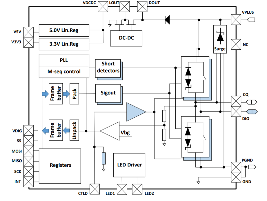
ST Microelectronics is bringing a bridge between a microcontroller capable of sensing/actuation and a 24 V power supply in industrial sensor applications with the L6364Q, a dual-channel transceiver IC, which brings dual communication channels, allowing for a configurable output with extra driving power, along with support for IO-Link, a DC / DC converter and a dual-mode UART.
The L6364Q transceiver IC brings some interesting hardware to the table: from linear and DC-DC regulators to configurable limiting current thresholds and many, many protection measures. As stated, the transceiver supports IO-Link (at COM2, with 38.4 kbaud and COM3, with 230.4 kbaud), as well as standard Single-Input / Output communication. In normal operation, the L6364Q is configured by the microcontroller at startup, through SPI. Then, it operates as a Single Input Output IO-Link device, controlling the input lines configured by the microcontroller. The device can also act as a physical layer between the microcontroller and an IO-Link master, which, when connected to it, the master can communicate with the microcontroller.
Regarding features, the L6364Q transceiver has:
Supply voltage range from 5 to 35 V
Linear regulators (5 and 3.3 V, at 50 mA current)
DC-DC regulator with configurable frequency (ranging from 0.5 MHz to 2 MHz) and voltage (from 5 to 10.5 V), with 50 mA current
Low dissipative (5 ohm) output stages for CQ and DIO, configurable in high side, low side or push / pull. Switching time of 100 ns (load of 2 kohm // 2.2 nF)
Configurable current limitation threshold for the CQ and DIO lines (from 110 mA to 250 mA) and in join mode (from 220 mA to 500 mA)
Full set of protection measures:
Embedded reverse polarity diode on the DOUT pin
Full zero current reverse polarity between the Vplus, CQ, DIO and PGND pins
Configurable thermal shutdown threshold, up to 216 ºC
7-bit temperature measurement, calibrated
Configurable undervoltage protection on the Vplus pin (from 6.0 to 15 V)
Operating voltage ranging from -40 to 150 ºC
Capable of driving inductive, resistive and capacitive loads
Quartz-free IO-link clock extraction and timing generation for the COM2 (38.4 kBaud) and COM3 (230.4 kBaud)
Integrated UART with M-sequence handling (checksum included) for the IO-Link sequences according to version 1.1 of the specification
Single octed UART mode for unlimited M-sequence size and continuous data transfer
Internal data buffer of up to 15 octets
Transparent UART mode for special applications
8 V zener for fast demagnetization of inductive loads
Two configurable LED drivers (up to 8 mA current)
QFN-20L 4×4 mm package
Block diagram of the L6364Q transceiver IC
Besides the aforementioned set of features, the transceiver guarantees ESD (for up to 4 kV) and EMC (2 A / 50 us, with 500 ohm coupling) protection. It has possible uses in industrial sensors and actuators, factory automation, process control, and as a switch driver of resistive, inductive, and capacitive loads, among other things. Lastly, it comes at a price of around $4.83.
Vecow Co., Ltd., a team of global embedded experts, announced the release of the latest Industrial Multi-Touch Computer, MTC-8000 Series. Powered by energy-efficient Intel Atom™ x7-E3950 processor with Intel® HD Graphics 505 chipset, MTC-8000 Series provides astounding 3D rendering, media composting and video encoding and brings more powerful system performance than ever.
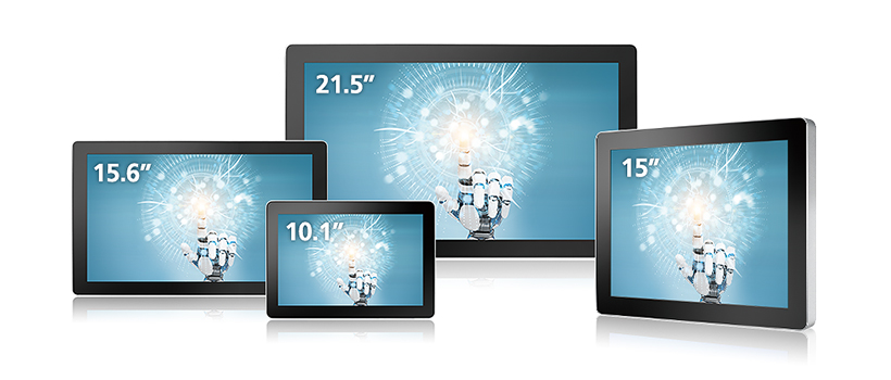
Vecow MTC-8000 Series offers a variety of display sizes from 10.1” to 21.5″ LED backlight control type industrial-grade LCD. It also features projected capacitive touch technology with 10-point multi-touch function for highly responsive sensing and has up to 7H hardness anti-scratch touch surface. Designed with a truly flat surface, Vecow MTC-8000 Series prevents water and dust accumulation on the system and allows for easy cleaning after each use.
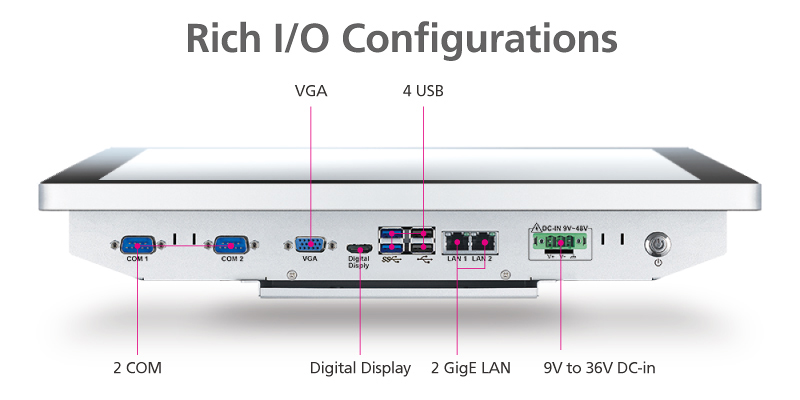
Vecow MTC-8000 provides various I/O ports including 4 USB ports, 2 Intel GigE LAN, 2 COM with RS-232/422/485, an easy-access 2.5” SATA SSD/HDD and a full-size mSATA for data storage that fulfills customers’ needs in each application. Users could also use internal mini PCIe to install 3rd party wireless modules, such as 4G/3G/LTE/GPS/WiFi/Blue tooth devices or expansion I/O modules to satisify customers’ requirements in various environments. The MTC-8000 Series also provides panel mount, VESA mount and Stand kit for easy deployment in diverse industrial environments. Vecow MTC-8000 Series is the best selection to build systems, self-service control panels, outdoor Kiosks and many other industrial applications.
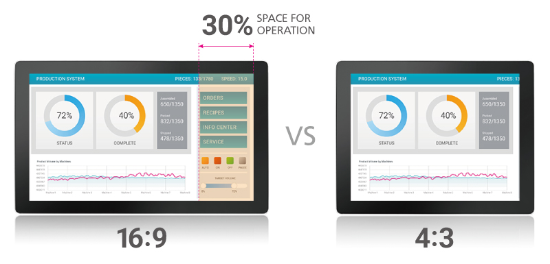
“Vecow MTC-8000 Series comes with a widescreen design that provides more operation area than standard 4:3 LCD with more space to process data, “
said Alan Chou, Senior Product Manager, Embedded Systems & Platform Division at Vecow.
“It also provides external SSD/HDD kit for easy system maintenance. With flexible expansion I/O ports to expand or integrate with 3rd party peripheral modules, our product design concept not only uses for traditional rugged automation field, but also light automation applications like Kiosk, Self-service system, and Signage applications”
“We are excited to introduce this low power consumption MTC-8000 Series Panel PC with features of thin, light, and elegant ID design to our partners,” said Joseph Huang, Sales Manager, Sales & Marketing Division at Vecow. “This system without a doubt provides reliable and trusted configurations, satisfies customers’ needs and improves the partnership with our customers.”
Powered by Intel Atom™ x7-E3950 processor, flexible product selection, outstanding performance, versatile I/O interfaces and industrial-grade reliability design, Vecow MTC-8000 Series is an ideal solution for AOI, HMI, Smart Retail, AGV Truck, Security, and any AIoT/Industry 4.0 applications.