VIA Launches VIA VAB-950 Board Powered by MediaTek i500 AIoT Platform

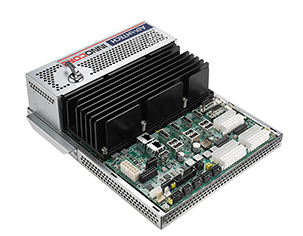
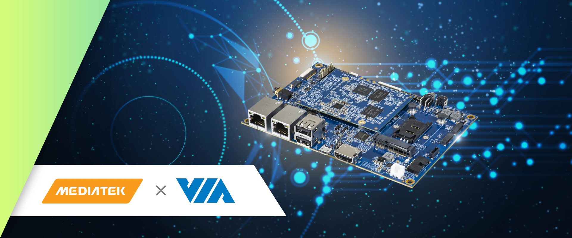
VIA Technologies, Inc. today announced the launch of the VIA VAB-950 board powered by the MediaTek i500 AIoT platform. Combining high-performance AI technology for display, object recognition, and voice with rich wireless and I/O connectivity features, the board accelerates the development of groundbreaking smart devices for myriad home, commercial, industrial, and educational use cases.

“As AI moves increasingly to the edge, the demand for smart devices with powerful edge processing, computer vision, and multimedia capabilities is growing at an unprecedented rate,” commented Richard Brown, VP of International Marketing, VIA Technologies, Inc. “The VIA VAB-950 provides the fastest and most dependable path for taking advantage of this huge market opportunity by creating innovative devices that deliver unique user experiences.”

”Over the next few years, we foresee very strong demand for powerful and efficient AIoT chipsets to enable the next generation of AI voice and vision devices,” said Henry Yeh, Assistant General Manager of the AIoT Business Unit at MediaTek. “With the new VIA VAB-950 board, powered by MediaTek’s i500 AIoT chipset, brands can speed up development time and bring to market innovative, differentiated devices for a wide range of applications.”

Highlights

  • Highly-integrated EPIC form factor with rich processing, wireless and I/O connectivity features
  • MediaTek i500 AIoT Platform with powerful edge processing, computer vision, and multimedia capabilities
  • Accelerates development of innovative Edge AI devices delivering unique user experiences

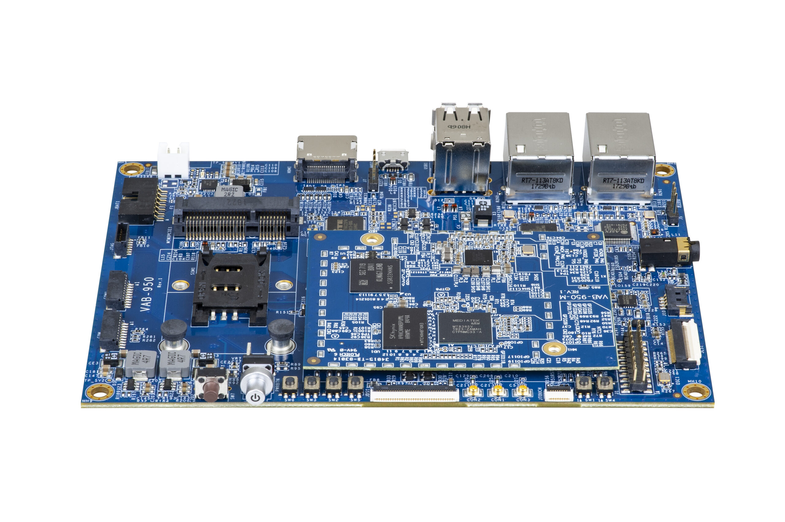
About the VIA VAB-950

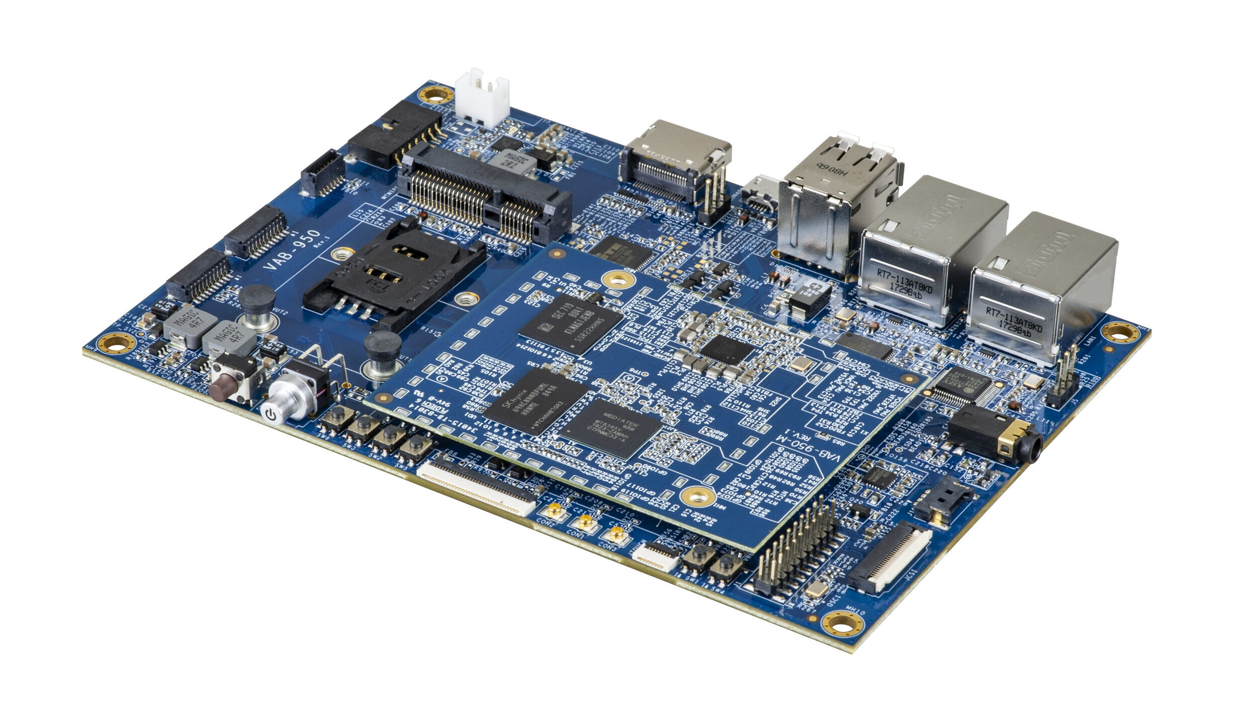
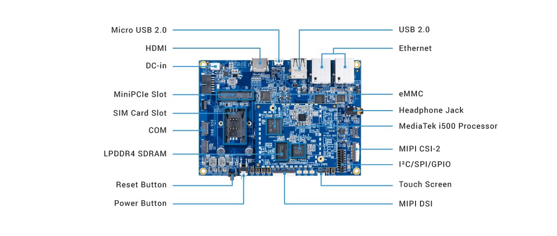
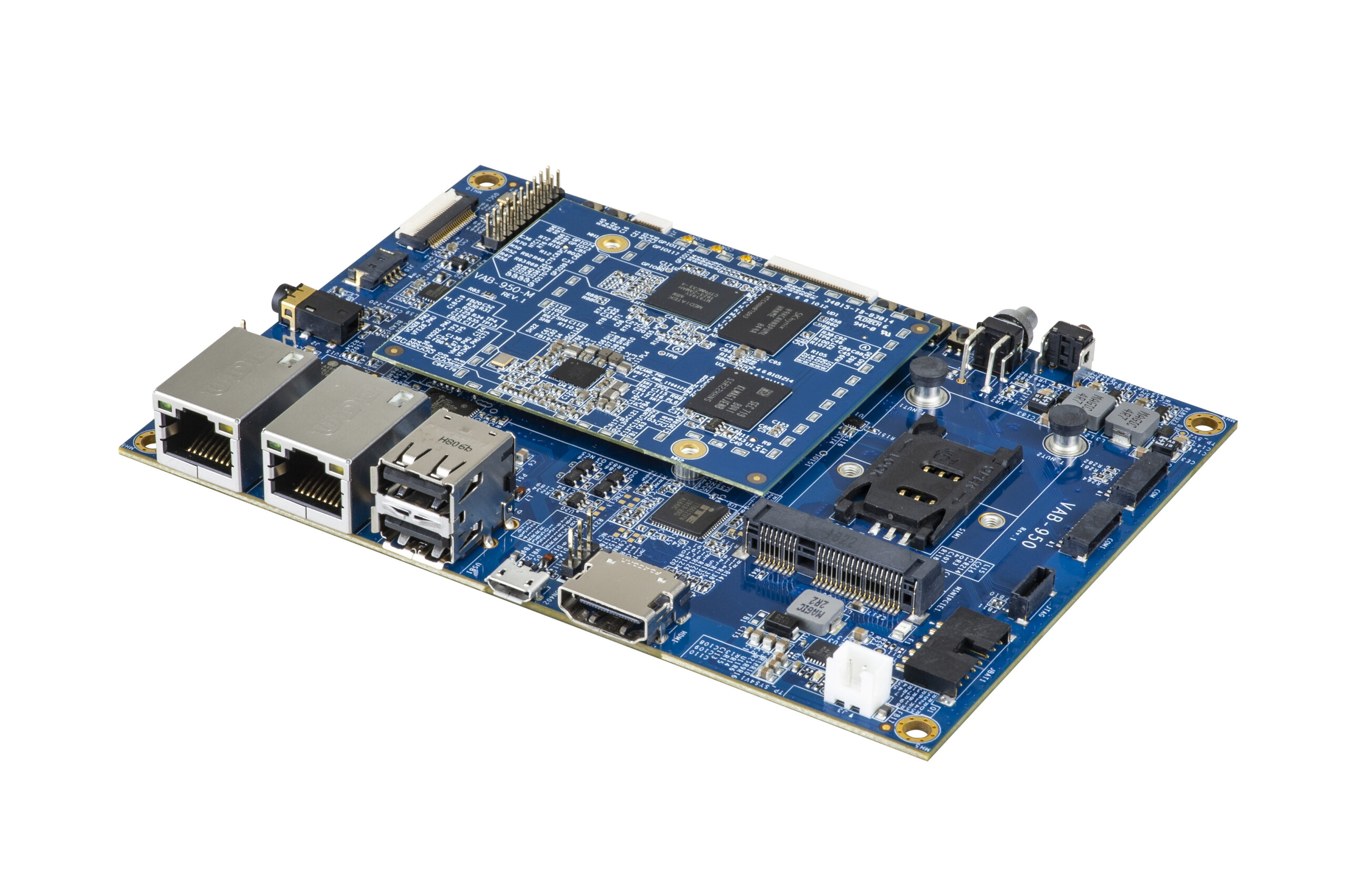
The VIA VAB-950 based on an EPIC 14cm x 10cm form factor and is available for sale worldwide now. The board’s key features include:

  • MediaTek i500 octa-core processor with integrated AI processor supporting high-performance edge processing, advanced multimedia capabilities, multiple high-resolution cameras, connected touchscreen displays, and multi-tasking
  • Advanced wireless and network connectivity including SIM card slot for LTE/4G, dual-band 802.11ac Wi-Fi, two Fast Ethernet ports, and Bluetooth 5.0
  • Rich I/O features including one USB 2.0 port, one RS232 COM port, and HDMI, MIPI DSI and MIPI CSI-2 display and camera support
  • Storage including 16GB eMMC 5.1 flash memory
  • EPIC 14cm x 10cm form factor
  • Yocto 2.6 and Android 10 BSP

A full set of hardware and software customization services that speed up time to market and minimize development costs is also available.

Learn more about the VIA VAB-950 here: https://www.viatech.com/en/products/boards/embedded-boards/vab-950/

Caltech Researcher Unveils Sensor that Rapidly Detects COVID-19 Infection Status, Severity, and Immunity

One feature of the COVID-19 virus that makes it so difficult to contain is that it can be easily spread to others by a person who has yet to show any signs of infection. The carrier of the virus might feel perfectly well and go about their daily business—taking the virus with them to work, to the home of a family member, or to public gatherings.

A crucial part of the global effort to stem the spread of the pandemic, therefore, is the development of tests that can rapidly identify infections in people who are not yet symptomatic.

Now, Caltech researchers have developed a new type of multiplexed test (a test that combines multiple kinds of data) with a low-cost sensor that may enable the at-home diagnosis of a COVID infection through rapid analysis of small volumes of saliva or blood, without the involvement of a medical professional, in less than 10 minutes.

The research was conducted in the lab of Wei Gao, assistant professor in the Andrew and Peggy Cherng department of medical engineering. Previously, Gao and his team have developed wireless sensors that can monitor conditions such as gout, as well as stress levels, through the detection of extremely low levels of specific compounds in blood, saliva, or sweat.

Gao’s sensors are made of graphene, a sheet-like form of carbon. A plastic sheet etched with a laser generates a 3D graphene structure with tiny pores. Those pores create a large amount of surface area on the sensor, which makes it sensitive enough to detect, with high accuracy, compounds that are only present in very small amounts. In this sensor, the graphene structures are coupled with antibodies, immune system molecules that are sensitive to specific proteins, like those on the surface of a COVID virus, for example.

Previous versions of the sensor were impregnated with antibodies for the hormone cortisol, which is associated with stress, and uric acid, which at high concentrations causes gout. The new version of the sensor, which Gao has named SARS-CoV-2 RapidPlex, contains antibodies and proteins that allow it to detect the presence of the virus itself; antibodies created by the body to fight the virus; and chemical markers of inflammation, which indicate the severity of the COVID-19 infection.

“This is the only telemedicine platform I’ve seen that can give information about the infection in three types of data with a single sensor,” Gao says. “In as little as a few minutes, we can simultaneously check these levels, so we get a full picture about the infection, including early infection, immunity, and severity.”

Established COVID-testing technologies usually take hours or even days to produce results. Those technologies also require expensive, complicated equipment, whereas Gao’s system is simple and compact.

So far, the device has been tested only in the lab with a small number of blood and saliva samples obtained for medical research purposes from individuals who have tested positive or negative for COVID-19. Though preliminary results indicate that the sensor is highly accurate, a larger-scale test with real-world patients rather than laboratory samples must be performed, Gao cautions, to definitively determine its accuracy.

With the pilot study now completed, Gao next plans to test how long the sensors last with regular use, and to begin testing them with hospitalized COVID-19 patients. Following in-hospital testing, he would like to study the suitability of the tests for in-home use. Following testing, the device will need to receive regulatory approval before it is available for widespread use at home.

“Our ultimate aim really is home use,” he says. “In the following year, we plan to mail them to high-risk individuals for at-home testing. And in the future, this platform could be modified for other types of infectious disease testing at home.”

The paper describing the research, titled, “SARS-CoV-2 RapidPlex: A Graphene-based Multiplexed Telemedicine Platform for Rapid and Low-Cost COVID-19 Diagnosis and Monitoring,” has been published online and will appear in the December issue of the journal Matter. Co-authors are former postdoctoral scholar in medical engineering Rebeca M. Torrente-Rodríguez, medical engineering graduate students Heather Lukas, Jiaobing Tu (MS ’20), Jihong Min (MS ’19), Yiran Yang (MS ’18), and Changhao Xu (MS ’20); and Harry B. Rossiter of the Harbor-UCLA Medical Center.

Funding for the research was provided by the National Institutes of Health; the Tobacco-Related Disease Research Program, a California state agency focused on reducing tobacco use; the Merkin Institute for Translational Research; and the Translational Research Institute for Space Health. Additional research support was provided by the Kavli Nanoscience Institute.

Advanced ultrasound-on-chip opens new applications

Ultrasound technology company Butterfly Network has announced its next-gen whole-body ultrasound product featuring its ultrasound-on-chip technology.

Butterfly Network, Inc. is once again reinventing ultrasound technology by delivering groundbreaking performance with fast, sharp imaging and unparalleled efficiency through its next-gen product, the new Butterfly iQ+, featuring the world’s only Ultrasound-on-Chip™ technology. Butterfly iQ+ offers new capabilities, such as faster frame rates, Needle VizTM technology, a longer battery life and industry-leading durability.

Butterfly’s mission is to democratize healthcare by making medical imaging accessible to everyone around the world. From underserved communities in the United States to remote areas around the globe, 4.7 billion people lack access to medical imaging. Putting ultrasound on a chip, Butterfly was able to define a new precedent of affordability by providing a whole-body ultrasound device at $1,999, plus membership. Today, as it reinvents ultrasound again, Butterfly iQ+ will be available for the same affordable price.

“Two years ago, Butterfly introduced the world’s first handheld, single-probe, whole-body ultrasound system. Since then, the device has been used by tens of thousands of medical professionals across the globe with significant clinical, economic and societal impact,” said Laurent Faracci, Butterfly Network’s Chief Executive Officer. “We have collaborated with the Butterfly community of users to define our innovation path. The first result in that journey is the new Butterfly iQ+, a big step forward for point-of-care ultrasound, with our most advanced chip ever and a number of amazing innovations and improvements that our talented team and partners developed.”

Butterfly iQ+ features an optimized manufacturing process in partnership with TSMC, the largest and most advanced dedicated IC foundry in the world. TSMC’s MEMS (microelectromechanical systems) manufacturing technology enables the ultrasound transducer to seamlessly integrate with CMOS (complementary metal-oxide semiconductor) technology. In addition, TSMC possesses manufacturing capacity that can scale to realize Butterfly’s vision of making an ultrasound device as ubiquitous as the stethoscope for the world’s 40 million healthcare providers.

Butterfly’s innovative product has been shown to be a particularly useful tool during the global COVID-19 pandemic due to its lung imaging capabilities, portability and ease of cleaning, as infection control has become increasingly important. Butterfly iQ+ brings a suite of new capabilities that make it even easier to make fast decisions at the bedside.

“These new capabilities bring us one step closer to realizing the full potential of bedside point-of-care ultrasound as the stethoscope of the future—a true window into the body,”

said Dr. John Martin, Butterfly Network’s Chief Medical Officer.

Faster, sharp imaging

With patented on-chip digital micro-beamforming enabling 15% faster frame rates and 60% faster pulse repetition frequency, healthcare providers can see image details in the heart, lungs and bladder with optimized clarity. High-performance shallow imaging capabilities help support fast, confident interventional decision-making, while deep imaging capabilities in the lung and deep cardiac presets allow for sharp details. The Butterfly iQ+ can help healthcare providers save time in their diagnosis and treatment of patients, improving overall patient outcomes.

State-of-the-art technology for new levels of control

The cutting-edge Needle VizTM technology available on Butterfly iQ+ can provide healthcare professionals with an enhanced ability to see a needle—improving confidence for central line placements, regional nerve blocks and other guided procedures. Additionally, in just four seconds, clinicians can calculate bladder volume automatically using the AI-based Auto Bladder Volume tool, allowing faster decisions at the bedside.

More power and durability

The Butterfly iQ+ extends battery life by 20% and scanning time by 100% to help healthcare providers get through their shift. With its durable, anodized aluminum body and replaceable compression- and stomp-tested cable, the Butterfly iQ+ offers military-grade durability to withstand tough shifts, and has been tested to withstand an industry-leading 4-foot drop. This next-generation device has gone through rigorous testing to ensure shock resistance and protection from dust and water damage.

OMZLO Programs the new TinyAVR MCUs

OMZLO has posted details about baremetal programming on the new TinyAVR MCUs. In their blog post, they describe how to program a blinky firmware on an Attiny406, from the ground up, using the simplest tools. Most of the things described can be easily transposed to other TinyAVR MCUs. About the programming, they say:

“Our approach is generally guided toward macOS or Linux users, but should also be applicable in an MS-Windows environment with a few minor changes.”

Even though OMZLO has been mainly focussing their development efforts on newer 32-bit Arm-Cortex chips (STM32 and SAMD), which typically offer more RAM, more speed, more peripherals, at a similar or lower price-point than older 8-bit MCUs, they decided to use the 8-bit MCUs which are substantially simpler to program.

connection diagram for firmware upload

Regarding the hardware, they decided to work with the Attiny406, with a view of using it in the future to replace the Attiny45 they currently use on the PiWatcher, which is their Raspberry-Pi watchdog. The Attiny406 enables 4K of flash space, 256 bytes of RAM, and can run at 20Mhz without an external clock source. We should note that one of the most important differences between the new TinyAVR MCUs and the older classic AVR MCU like the Attiny85 is that the newer chips use a different programming protocol called UPDI, which requires only 3 pins, as opposed to the 6-pin ISP on the classic AVRs. A little research shows that programming TinyAVRs with UPDI can be achieved with a simple USB-to-serial cable and a resistor, thanks to a python tool called pyupdi.

Schematics

For the schematic, they created a minimalistic breakout board for the Attiny406. The board can be powered by 5V through USB or a lower 3.3V through dedicated VCC/GND pins. They also equipped the board with LED and a button was also fitted on the board, and for testing purposes, they decided to embed the 4.7K resistor needed for the UPDI programming directly in the hardware (i.e. resistor R2). The resulting breakout board is tiny and fits conveniently on a small breadboard. The design files are shared on aisler.net. When you want to Program the Attiny406 on the board with a USB-serial cable, you just connect the headers on the board edge.

The Breakout Board

For software, they installed pyupdi following the instructions provided on their webpage. They also connected the USB-Serial cable to the board with the 4 dedicated UPDI pins available on the board. After installing the software, the USB-Serial converter shows up as the file /dev/tty.usbserial-FTF5HUAV on a MacOS system. To test that the programmer recognizes the Attiny406, you can issue a command similar to the following, adapting the path for the USB-serial converter to your setup: pyupdi -d tiny406 -c /dev/tty.usbserial-FTF5HUAV -i This should result in the following output if all goes well: Device info: {‘family’: ‘tinyAVR’, ‘nvm’: ‘P:0’, ‘ocd’: ‘D:0’, ‘osc’: ‘3’, ‘device_id’: ‘1E9225’, ‘device_rev’: ‘0.1’}

With the right tools, bare-metal programming on the new TinyAVR MCUs is as simple as on its older AVR cousins. You can find more information on OMZLO’s blog post. If you have programming tips for the AVRTiny, you can also share it with them on Twitter.

Laird Connectivity Sentrius MG100 Multi-wireless IoT gateways with LTEM/NB-IoT and Bluetooth 5

The creation of a sensor network can result in an overwhelming amount of work. From deciding on the perfect technologies to making your prototype and ensuring it is secure, it usually is a demanding task. But what if there was a way to simplify this process? There is, actually, the new Sentrius MG100 Gateway from Laird Connectivity promises to give you an important boost when it comes to developing your next IoT application!

The Sentrius MG100 from Laird Connectivity is a multi-wireless IoT gateway, designed with the Bluetooth 5 and LTE-M / NB-IoT technologies. Making use of the Pinnacle 100 Modem from the company, it captures data from Bluetooth 5 long-range sensors and sends it to the cloud via a low power cellular connection (LTE-M / NB-IoT). It comes with a starter kit so that you can quickly set up projects, including their innovative BT510 multi-sensor platform, with Bluegrass Cloud portal so that your end-to-end IoT solution can be work seamlessly out of the box.

Regarding its specifications, the Sentrius MG100 Gateway packs:

  • Bluetooth: BT 5.0 (single-mode, 4x range, 2x speed, LE advertising extensions), concurrent master, slave, BLE mesh capabilities, BT 4.2 (LE secure connections, data packet length extension, LE privacy) and BT 4.1 (LE dual-mode topology, LE ping)
  • Cellular: Multicellular band operation for world-wide compatibility, LTE M and NB-IoT support, power class 3
  • Nordic nRF52840 Cortex-M4F MCU
  • Memories: 256 KB RAM and 1 MB onboard Flash (with support for SD card)
  • NFC (13.56 MHz, 106 kbps data rate, NFC Type2 and Type4 tag emulation)
  • Built-in accelerometer
The sleek kit (1x MG100 Gateway + 3x BT510 multi-sensors)

Besides the interesting set of features discussed before, the MG100 Gateway allows you to create an application tailored to your needs, as you can program the ARM Cortex-M4F microcontroller with the simple, yet powerful Zephyr RTOS, enabling you to customize it to your liking. You can also take advantage of the sample application database for the MG100 to easily connect and send data to the AWS platform. Regarding power, you can power it with an USB external power supply and acquire optionally a rechargeable backup battery to be safe in case of a short-term power outage. There is some degree of customizability when it comes to the antenna, where you can use the low-cost internal LTE and BT antennas or opt for external ones, that may suit your working environment. Lastly, since security is important these days, their bootloader architecture creates secure devices that only run approved software. 

When it comes to applications, there is a lot you can do with this kit: from cold chain monitoring to smart buildings, industrial IoT, and transportation, its value as a product is immense. Coming at a price of $256, you pay for the time boost it will give you. As a reminder, the kit comes with 1x Sentrius MG100 Gateway, 3x Sentrius BT510 multi-sensors, and 3x regional power supplies.

Laird Connectivity MG100 Gateway Mouser link: https://eu.mouser.com/ProductDetail/Laird-Connectivity/455-00120?qs=GedFDFLaBXEsRDGPg0N3Hg%3D%3D

Multi-sensor predictive maintenance kit with IO-Link stack v.1.1

Are you on the market for a kit ready to kickstart your predictive maintenance projects? Probably you may want to hear about the IO-Link stack v.1.1 from ST microelectronics, as they just released this very complete and interesting kit, in a very compact form factor. There is just about everything you need, including sensors, processing capabilities, and communication. Overall, we are looking at a very solid package.

The STEVAL-BFA001V2B is an industrial reference kit for condition monitoring predictive maintenance, ready to be deployed in industrial environments, by obeying the IEC61000-4-2/4 and EN60947 requirements for these environments. This board was specifically designed for industrial applications, housing industrial sensors, along with the necessary debugging tools, cables, adapters, and plugs for applications that need industrial communication. This module connects through a standard multipolar cable, where one wire is being used for IO-Link data.

But regarding the specifications, what are we looking at? Let us see:

  • Kit: sensor node (STEVAL-IDP005V2, not available separately), communication board (STEVAL-UKI001V2, not available separately) and STLINK-V3MINI programming and debugging interface
  • Supply voltage range from 18 to 32 V
  • Sensor node:
    • ARM Cortex-M4 microcontroller for signal processing and analysis (STM32F469AI)
    • IIS3DWB: ultra-wide bandwidth (up to 6 kHz), low-noise 3-axis digital vibration sensor
    • LPS22HB: absolute digital pressure sensor
    • HTS221: relative humidity and temperature sensors
    • IMP34DT05: digital microphone sensors
    • L6362A: IO-Link PHY device
    • EEPROM for data storage
    • Step-down switching (L6984) and LDO (LDK220) regulators
    • ESD protection
  • M12 standard industrial connector
  • SWD connector for programming and debugging purposes
  • Reset button and expansion connector with GPIO, ADC, I2C bus and timers
  • Designed to comply with the IEC industrial standard requirements
Block diagram for the STEVAL-BFA001V2B sensor node

Besides the robust set of hardware, there is also great firmware support. The STSW-BFA001V2 firmware package (available for free on the ST website) includes algorithms for advanced signal processing and analysis in the time and frequency domains (FFT with programmable size, programmable windowing, speed RMS moving average, and thresholds for warning and alarm), for the high bandwidth 3D digital accelerometer in vibration monitoring applications. But it does not stop there, you get also some microphone algorithms, including PDM to PCM, SPL (sound pressure level), and audio FFT.

Overall, this is a solid packaging, made up not only by hardware but also the firmware provided by ST, which comes with very complete examples that can provide you with a nice jump when starting the development. Regarding applications, the supply voltage can be a bit dissuasive, but that may not be a problem in an industrial environment, which is its purpose. Although, it would be nice to have some smaller voltage options. Lastly, the pricing is acceptable, considering the number of components condensed in a considerably small size ($145).

STEVAL-BFA001V2B link: https://www.st.com/content/st_com/en/products/evaluation-tools/product-evaluation-tools/mems-motion-sensor-eval-boards/steval-bfa001v2b.html?icmp=tt15190_gl_bn_apr2020#overview

Advantech Introduces the First All-In-One Gaming Platform with Intel Iris Xe graphics

Advantech-Innocore the gaming-focused business group of Advantech Corp, announces the new DPX®-E145 gaming system. The DPX-E145 is a complete gaming system for the regulated casino and AWP gaming markets combining all the hardware features necessary for a gaming platform together in a high performance industrial grade system.

Breaking new ground in integrated graphics performance, the new 11th generation Intel Core processors with Intel Iris Xe graphics allows the DPX-E145 to meet the ever-increasing demands placed on casino slot machines for a multi-screen, high resolution, immersive player experience.

At the heart of the DPX-E145 is the 11th Generation Intel Core processor, which includes high performance dual and quad core CPUs up to Dual Core @ 3.0GHz (3.9GHz max turbo), Quad Core @ 2.8GHz (4.4GHz max turbo) and sporting massive cache up to 12MB. The system is supplied with up to 64GB DDR4 PC3200 system RAM, and the DPX-E145 is ready for mission critical applications that require an ECC memory option.

Highlights

  • 11th Generation Intel® Core™ SOC CPUs
  • CPUs up to Dual 3.0 (3.9) GHz, Quad core 2.8GHz (4.4) GHz
  • Intel Iris Xe integrated graphics
  • Four 4k monitor support
  • Comprehensive gaming features
  • Passive cooled system up to 28W
  • 12V DC single input or ATX power

The “Discrete-level Graphics” core (Intel Iris Xe graphics) outputs to four independent monitors via four DisplayPort DP++ ports. The graphics engine features the latest Intel Xe architecture with up to 96 graphics execution units, providing unrivalled performance and features including Direct X 12, OpenGL 4.5, OpenCL 2.2 and support for video decoding HEVC/VP9/SCC (10 bit). The new display engine is optimized for four 4K displays at 60Hz but also supports two 8k displays at 60Hz.

Even with the unprecedented high performance, the DPX-E145 is passive-cooled requiring no CPU fan in most applications and therefore reducing maintenance costs for potential fan failures in the field.

The DPX-E145 is designed with the same format as the other E series products (DPX-E135, DPX-E140) and has the same “Cabinet-ready I/O”. This innovative design puts all the connectors conveniently in one area and uses typical slot machine industry connectors to provide an economical, robust harnessing design. The need for additional connector boards or backplanes is eliminated saving cost and simplifying cabinet layout and harnessing.

A full feature set of I/O and COMs designed specifically for gaming devices is also included and the system is compatible with Advantech’s software solutions for security, media validation, SAS and diagnostics.

A wide variety of storage devices are supported including SATA DOM, C-Fast, M.2, USB drive and the system has a built in easy-service tray for 2.5” SATA SSDs.

The DPX-E145 is the ideal integrated platform for many gaming, amusement and kiosk applications calling for a very high-performance gaming platform backed by the reliability and longevity only available from Advantech and Intel.

Key features

  • Dual and Quad Core 11th Gen Intel Core CPUs up to: Dual Core @ 3.0GHz (3.9 GHz max turbo), Quad Core @ 2.8GHz (4.4GHz max turbo)
  • Intel Iris Xe high performance graphics with Core i5 and i7 CPUs (i3 have Intel UHD for 11th Gen. Graphics cores)
  • Four independent monitors supported (4 x 4K60)
  • Comprehensive gaming features including dedicated ports for CCTALK, SAS, GPIO, I2C, meter connect, ID003, RS485, and 5.1 surround sound.
  • Passive cooled system up to 28W
  • 12V DC single input or ATX power
  • “Cabinet-ready” I/O connectors on-board
  • Casino grade lock and intrusion monitoring (Battery backed and logged)
  • Long lifecycle (guaranteed 7 years in production)

Craig Stapleton, Advantech’s Product Director, commented,

“Following the success of our DPX-E135 and DPX-E140 products with ‘Cabinet-ready I/O,’ we are pleased to be able to bring customers a high performance follow on product, the DPX-E145. The DPX-E145 is one of the first products to utilize the latest 11th Generation Intel Core architecture that is the first to offer the revolutionary Intel Iris Xe graphics core. Xe graphics with up to 96 execution units supports 8K displays or 4 simultaneous 4k displays. The new Iris Xe graphics has proved very impressive in consumer markets and we are excited to bring it to our gaming customers. Intel Iris Xe graphics with up to 96 execution units that will deliver up to 2.95x the graphics performance of 8th Gen Intel® Core™ processors note 1. This performance increase of this amazing graphics engine means more gaming customers can dispense with the need for a discrete graphics card. The DPX-E145 will be an unbeatable combination for the gaming OEM”.

more information: www.advantech.com

Axiomtek’s RISC-based DIN-rail Fanless Embedded System – Agent200-FL-DC

Axiomtek – a world-renowned leader relentlessly devoted in the research, development and manufacture of series of innovative and reliable industrial computer products of high efficiency – is unveiling the Agent200-FL-DC, an extremely compact RISC-based DIN-rail industrial IoT gateway. The ultra-low power embedded box PC is powered by the NXP i.MX 6UL processor with the ARM® Cortex™-A7 microarchitecture. Designed to meet the challenges of harsh operating environments, it supports extended operating temperature range of -40°C to 70°C, a flexible wide voltage range of 9V to 48V DC power input, and can withstand high vibration environments up to 2G. With the ability to transmit data and manage various devices, the versatile gateway is optimized for remote control and monitoring management applications such as unmanned control rooms, industrial machines, automatic parking lots, traffic monitoring systems, etc.

The Agent200-FL-DC offers operational reliability, rugged design, rich features and easy maintenance. Two PCI Express Mini Card slots, one SIM card slot and two internal antennas are available for Wi-Fi, 3G/4G and GPS connections.

“Based on the RISC architecture, the budget-friendly industrial gateway has lower heat output and lower power consumption, making it suitable for applications which demand a balance between power and performance,” said Tina Tu, product manager of Network Computing Platform Division at Axiomtek. “The built-in serial port, LAN port and USB port provide fast and efficient data computation, communication and acquisition. Besides, its digital input/output interfaces are available for a wide variety of test and measurement applications. The Agent200-FL-DC can be integrated anywhere through the DIN-rail mounting kit and wall mount bracket.”

The IP20-rated fanless gateway comes with a 256MB onboard DDR3L memory and one onboard 4GB eMMC for storage. The Agent200-FL-DC measuring only 31 x 100 x 125 mm has rich I/O interfaces including one switchable RS-232/422/485 port, one 10/100 Mbps LAN port, one USB 2.0 port, one digital I/O (4-in/4-out), and one CANBus port. The LED indicators on the front panel show the status of the device. The industrial-grade DIN-rail embedded platform is compatible with Yocto embedded Linux to provide an open standard operating system for software program development.

Advanced Features:

  • RISC-based (i.MX 6UltraLite) processor 528 MHz
  • 256MB DDR3L SDRAM onboard
  • 4GB eMMC flash onboard
  • 2 PCI Express Mini Card slots (Wi-Fi or 3G/4G)
  • 4 digital inputs and 4 digital outputs
  • Wide voltage range of 9V to 48V DC power input with terminal block
  • Embedded Linux (Yocto) operating systems
  • Fanless and compact design
  • Wide operating temperature range from -40°C to +70°C

Axiomtek’s Agent200-FL-DC will be available at the end of September 2020. For more product information or pricing, please visit our global website at www.axiomtek.com or contact one of our sales representatives at info@axiomtek.com.tw.

Challenges involved in 5G Testing

The imminent large-scale rollout of 5G technology imposes new and tough challenges for designers of PCB, network equipment and electronic devices in general. 5G will not only represent an increase in data rates, but it will be a real revolution, with latency times reduced up to 1ms and the use of millimeter waves (mmWave) to support greater bandwidth. PCBs for 5G mobile and network devices must be able to simultaneously manage higher digital data rates and higher frequencies, pushing mixed signal design to its limit. 5G applications will also pose a variety of new challenges for the engineers developing automated test equipment (ATE).

Compared to the current 4G mobile network, the rollout of 5G will force designers to rethink the layout of PCBs used in mobile devices, data transmission networks and IoT infrastructure. Ensuring signal integrity at every point on the board represents one of the most difficult challenges imposed by 5G testing. Due to the presence of mixed signals, it will be necessary to prevent EMI between the analog and digital sections of the board, verifying that the FCC EMC requirements are met.

Challenges involved in 5G Testing – [Link]

Nordic Semiconductor’s nRF52820 Multi-protocol SoC combines Bluetooth 5.2 with USB 2.0

Are you on the market for an SoC with advanced wireless connectivity in a really small package? Then, you should take a look at the Nordic Semiconductor nRF52820 SoC, that offers you advanced wireless connectivity and built-in USB 2.0, ready to size-down your awesome projects!

At first glance, nRF52820 seems like any other IC, but it gets more and more interesting when you dive into it. In its small package, there is an ultra low power, fully featured multiprotocol radio that is capable of handling all Bluetooth 5.2 has to offer (such as Bluetooth Low Energy, Bluetooth Mesh, Thread and Zigbee mesh protocols, along with directorion finding, high-throughput 2 Mbps and long-range features), full speed USB 2.0 capabilities, among other digital interfaces and analog capabilities.

Overall, we are looking at a very solid solution, especially when we look at its set of specs:

  • ARM Cortex-M4 clocked at 64 MHz
  • Memories: 256 KB Flash and 32 KB RAM
  • 1.7 to 5.5 V supply voltage range + integrated DC/DC regulator
  • Bluetooth Low Energy (Bluetooth 5.2 + Direction Finding + High throughput 2 Mbps + Long Range) and Bluetooth mesh
  • 802.15.4 protocols (Thread and Zigbee)
  • Ultra-low power 2.4 GHz multiprotocol radio (+8 dBm Tx power, -95 dBm Rx sensitivity, 4.9 mA in Tx mode at 0 dBm and 4.7 mA in Rx mode at 1 Mbps)
  • Security: 128-bit AES encryption
  • Digital interfaces: 12 Mbps Full Speed USB 2.0, UART, 2x SPI/TWI, QDEC
  • Other peripherals: Analog comparator, 4x 32-bit timer/counter, 2x 24 real-time counter, PPI, GPIOTE, temperature sensor, WDT and RNG
  • Extended operating temperature range (from -40 to +105 ºC)
  • package: 5 x 5 mm QFN40 with 18 GPIO pins
The hardware stack of the nRF52820 in greater detail

Regarding the SoC, it gives you some degree of freedom when it comes to powering your projects. Since you can supply it with voltages ranging from 1.7 to 5.5 V, both rechargeable batteries or USB are viable options. Its extended temperature range makes it useful in projects where temperature can be an issue, such as professional lighting applications. The Bluetooth 5.2 features it packs, along with its small form factor, makes it a viable asset in tracking applications, where the Direction Finding capabilities come in handy. Lastly, the fully-featured, built-in USB and the multiprotocol radio with +8 dB transmission power make it a suitable network processor to be paired along with application MCUs in gateways, smart home applicancies, commercial and industrial applications that require you to have advanced wireless connectivity. Overall, there are a lot of possibilities in such a tiny module.

The nRF52820 augments the already interesting nRF52 series, by Nordic Semiconductor, and chances are you already worked with one of those modules, which will help you reduce the time to market and increase the reusability of your software / decrease the development cost. Overall, we think it is an interesting module to dip your feet into Bluetooth 5.2. Considering the small cost of $4.34 for each module (or $48.48 for a development kit), you have nothing to lose. 

TOP PCB Companies