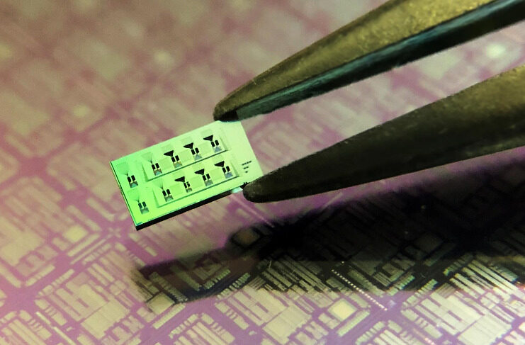
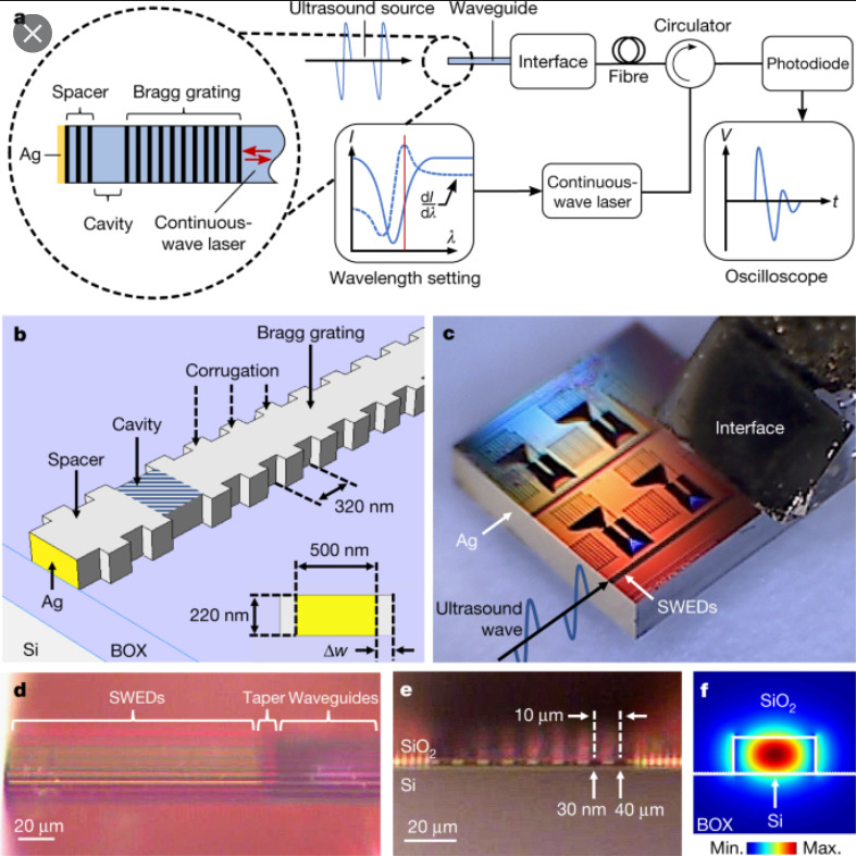
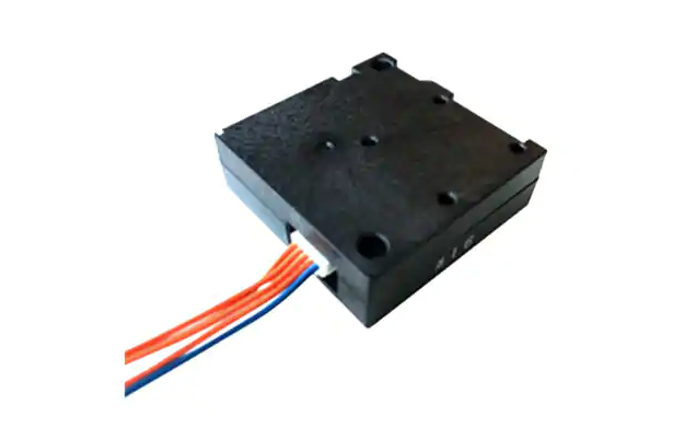
A group of researchers at the Helmholtz Zentrum München and the Technical University of Munich (TUM) have developed an ultrasound detector, based on silicon photonics and measuring a hundredth the width of a human hair. They claim it is the world’s smallest ultrasound detector. Rami Shnaiderman, developer of the SWED device says:
“This is the first time that a detector smaller than the size of a blood cell is used to detect ultrasound using the silicon photonics technology.” He continues “If a piezoelectric detector was miniaturized to the scale of SWED, it would be 100 million times less sensitive.” Its miniaturized photonic circuits which are undetectable to the human eye are assembled on top of a silicon chip. This has enabled the research team to develop the ultrasound detector.
The SWED works by monitoring the changing intensity of light as it passes through the photonic circuits that consist of the silicon chip, as opposed to recording voltages output by piezoelectric crystals, as with a conventional ultrasound detector. Ultrasound detection technology has always relied on piezoelectric detectors, which works by converting ultrasound wave pressure into electric voltage. The imaging resolution derived with the ultrasound depends on the size of the piezoelectric detector being used. When you reduce its size, it increases resolution, enabling smaller, densely packed 1D or 2D ultrasound arrays. The achieved arrays improve the chances of effectively discriminating features in imaged tissue and/or material. Decreasing the piezoelectric detector size, however, significantly impairs sensitivity, making the detectors unusable for practical application.
Talking about the edge SWED has over piezoelectric, Rami Shnaderman says:
“If a piezoelectric detector were to be miniaturized to the scale of SWED, it would be 100 million times less sensitive.”
This is because its size corresponds to an area that is over 10,000× smaller than the smallest piezoelectric detectors used in clinical imaging applications. Also, SWED is up to 200× smaller than the ultrasound wavelength employed in those clinical applications (a factor that allows it to visualize features less than 1 µm, or superresolution image).
Originally developed to propel optoacoustic imaging performance, the researchers however say there will be broader sensing and imaging applications of the SWED in the future. The SWED is principally aimed at clinical diagnostics and basic biomedical research, and also those in industry settings. Regarding the progress and refinement of the SWED, Shnaiderman says
“We will continue to optimize every parameter of this technology — the sensitivity, the integration of SWED in large arrays, and its implementation in hand-held devices and endoscopes.”
The researchers claim that a SWED can be manufactured at a tiny fraction of the cost of a piezoelectric detector. The team published an earlier paper on SWED technology and can be found here. You can find the research work here.
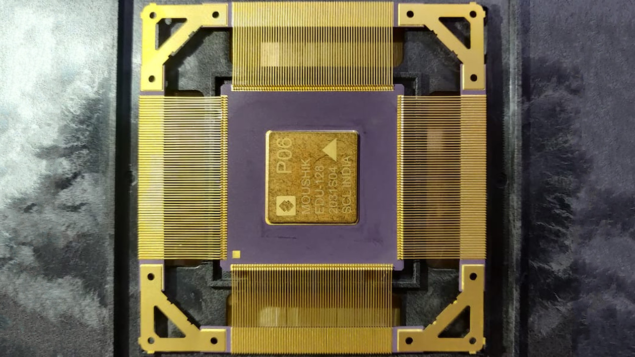
Researchers at IIT Madras have successfully booted up ‘Moushik‘, a microprocessor that has been indigenously designed and fabricated in India. The design was done in IIT Madras, the fabrication at the ISRO Semiconductor Laboratory in Chandigarh. So this is a complete made in India Microprocessor same as we saw with AJIT.
Moushik is the third series of chips that have been produced by The SHAKTI, which is a free and open-source silicon project from India. Moushik is a processor-cum-system on-chip that has an intended use in the rapidly growing Internet of Things IoT devices.
Built on a 180nm process, the Moushik has 103 functional IO pins across a 256 pin CQFP package. It is powered by the SHAKTI E-Class RISC-V core. The CPU runs at a clock speed of 75-100MHz, it supports many common peripherals like SDRAM controller, I2C, quad-SPI, analog-to-digital conversion (ADC), UART, and JTAG for debugging.
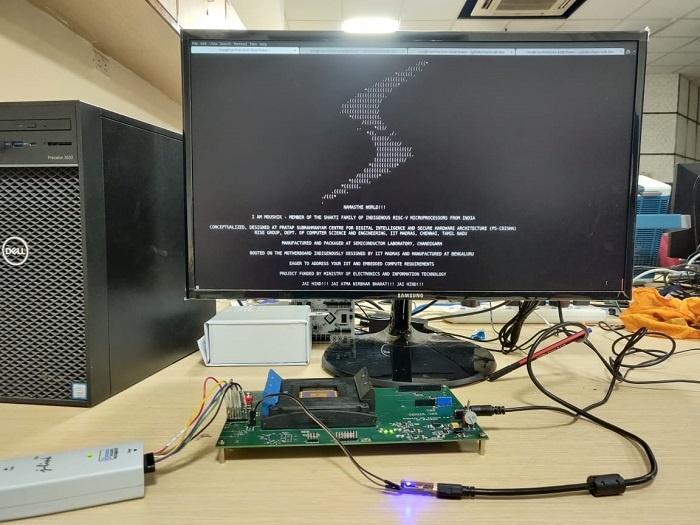
Boot up screen for the Moushik
The new SoC can find its suitable applications in Credit cards, ID Cards, Debit cards, Travel passes for Metros and Driving Licenses, Electronic Voting Machines (EVMs) attendance systems, surveillance cameras, safe locks, Personalized Health Management Systems, and Consumer Electronics.
The most exciting feature about the motherboard is that it has the support for Arduino shield add-ons for countless embedded developments. Besides, the motherboard also has switcher ICs. They enable power conversion across a large variety of voltages (12V-5V, 5v – 3.3V, 3.3 – 1.8V) to enable a variety of peripherals to be connected with the motherboard. The PCB is a four-layer board (1.6mm thickness) with an input power of 12 volt and 2 amp. It also has support for 512MB SDRAM.
IIT Madras mentions that the Shakti series Microprocessors can be used worldwide as it is on par with International Standards and can make its way to the global market. Because of their open-source nature, startups and industries can customize its design based on their requirements. Indigenous design, development, and fabricating also cuts down the risk of using (imported) systems.
Further information can be collected from the tape out and a YouTube video published by Shakti.
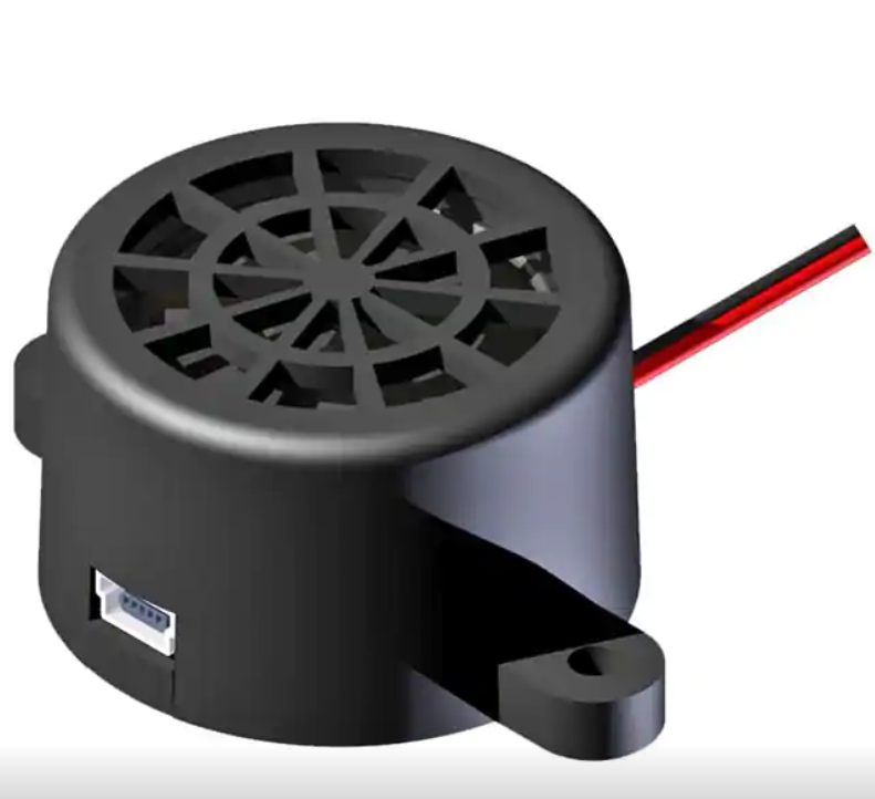
Did you ever make a project and wanted to output a sound that was more than just a beep? Or maybe you wanted to play a long song on repeat, such as an audio alert for when something is not working on a factory, or just to annoy your friends, your choice. An Audio Programmable Indicator is basically what you need, and the PUI API-4260-LW150-2-R might just be your best choice if you are out to get one!
But what does differentiate this product from other API’s? First off, it is extremely easy to use, even easier than normal. You can plug it in via USB to any computer (as it is recognized as a USB device), drag and drop an MP3 file, and you are set! Then it is ready to be integrated with your projects. All you have to do is power it and it will play your song on repeat when you power it.
But what is going on in there? Well, if you open it, and you can take a look at this process in the Adafruit’s video where they actually tear it down, there is a buck converter, along with a 4MB SPI flash chip and followed by an interesting, cheap IC that can basically only play MP3. From that point on, there is only the amplifier circuit and the speaker itself, aside from the USB port.
More about the specs:
12 V rated voltage, range from 7 to 24 V
350mA of current at rated voltage
Repeating tone/pulse
ABS housing material
Easy drag and drop file transfer on nearly any computer
150 mm lead wires and mounting flanges for easy integration
Wide frequency response (100 Hz to 20 kHz)
Mini USB-B port
What is so cool about it is its simplicity. How many projects have you just wanted to play a sound and this is probably the simplest way possible that does not suck! It can be used on projects where you need to alert, or even assist someone with audio. Even though the API is a simple product, there is a lot of utility in this little guy!
Lastly, let us talk about pricing: how much? Actually, is not a lot. This API is available on Digikey for $21.93. Now, could you DIY this for cheaper? Probably, but what you are getting, the simplicity in such a solid package may be enough to make you forget about the price. What do you think, will you pick it up? Where would you apply it?
“TinyML is proof that good things come in small packages”, or so does ARM describe it, as it promises with TinyML to change a different approach, by running optimized machine learning models on small and efficient microcontroller-based endpoint devices, instead of bulky, power-hungry computers located in the cloud. Supported by ARM and the industry-leaders Google, Qualcomm, and others, it has the potential to change the way we deal with the data gathered by the IoT devices, which already have taken over in almost every industry we can imagine.
But why would we use TinyML in microcontrollers? Well, that is simple. They are everywhere! Families such as the ARM Cortex-M are very efficient and reliable, guaranteeing decent computing performance, when we consider their size, fitting them anywhere and being able to leave them there and just forget about it. Moreover, they are really cheap. Machine learning on microcontrollers enables us to take care of the data created on our IoT devices directly and perform more sophisticated and refined operations. But it does not stop there. Giving these capabilities to the microcontroller allows for more independent endpoint devices, that do not require an internet connection to trade data back and forth with the cloud, which leads to reduced latency, less energy consumption and extra security, since the data is not leaving the microcontroller as often, leaving it less exposed to attacks.
In order to bring the ML algorithms to the small boards, the complexity of the mathematical operations involved needed to be reduced. Data scientists accomplished this by applying different techniques, such as replacing floating-point operations with simpler 8-bit operations. The changes resulted in models adapted to the platform, targeting lower memory resources and processing, making them work more efficiently without compromising too much accuracy. Of course, they cannot replace completely the cloud models, but its suits for many use cases. Besides that, the hardware is being designed by ARM to accelerate the inference, which will uplift the already impressive performance we are getting.
Machine learning on microcontrollers gives new powerful capabilities to our projects, having almost unlimited use cases. Developers are already making use of TinyML to solve issues of all sorts, including responsive traffic lights to reduce congestion, prediction of maintenance on industrial machinery, detection of dangerous insects in crop fields, in-store shelves that warn when the stock is low, private healthcare monitors… The list goes on.
The value of TinyML has been quickly recognized by the main industry players, who are helping to push the technology even further, from which we can highlight the collaboration between Google and ARM combining the ARM CMSIS-NN libraries with the TensorFlow Lite Microframework, helping non-experts in embedded programming get their hands on the technology. People like you and me, developers, can also join easily, all you need is a computer, a USB cable and a development board that can be acquired for as low as $15.
In most of our previous tutorials related to operational amplifiers, the configurations were based on amplifiers with resistors as part of the feedback loop, voltage dividers, or to interconnect many op-amps. This new tutorial presents a configuration called integrator in which a reactive component (capacitor) is added in the design.
In the first section, we will focus on the functioning of the integrator by showing how the capacitor affects the circuit and the AC response of the circuit is also presented. Moreover, we demonstrate its output voltage formula and highlight why this circuit can be labeled as an integrator.
The basic configuration presented in the first section presents limitations that are exhibited in the second section. “Real” or “Practical” integrator circuits are presented and we investigate how similar they are with their ideal equivalent.
Presentation
Functioning
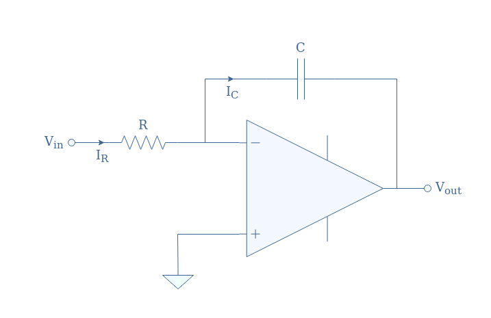
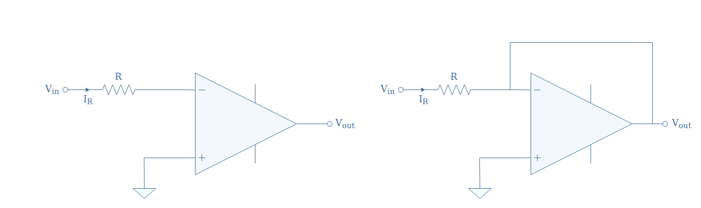
An integrator consists of an inverting op-amp in which the resistor present in the feedback loop is replaced by a capacitor. The basic design on an integrator is presented in Figure 1 below, we will also refer to this circuit as the ideal integrator.
fig 1: Integrator circuit representation
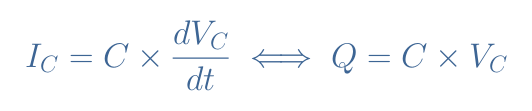
The behavior of the integrator is mainly dictated by the electric behavior of the capacitor. We remind in particular the constitutive equation of the capacitor:
eq 1: Constitutive equation of capacitors
With VC being the voltage across the capacitor, C its capacitance, and Q its charge.
From Equation 1, we can understand that a capacitor reacts to variations of voltage. Indeed, if no variation is happening, no current is observed but if the voltage across the capacitor varies, it discharges and lets the current pass.
In other words, in DC regime, a capacitor is equivalent to an open circuit while in the high-frequency regime it tends to be a short circuit as the frequency increases.
When we apply this observation in the context of the operational amplifier, we can see that in the DC regime the circuit of Figure 1 is equivalent to an op-amp in open-loop configuration (non-linear regime) and behaves therefore as a comparator.
However, when variations of the input are present, the circuit tends to be equivalent to an inverting buffer op-amp (refer to the tutorial Op-amp building blocks) as a negative feedback loop is established:
fig 2: Equivalent integrator circuit in DC regime (left) and in high-frequency regime (right)
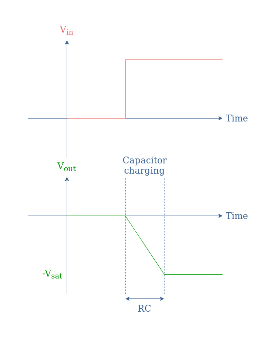
Keeping this behavior in mind, it is interesting to focus on how the integrator circuit reacts to a Heaviside input, which is also known as the step response:
fig 3: Step response of the integrator circuit
It is interesting to note that the saturation voltage Vsat limits the integration operation since the negative ramp of Vout should continue as long as Vin≠0.
AC response
The most important fact to keep in mind from Figure 3 is that a time limitation given by the value R×C exists for the amplifier to switch from one state to the other. In other words, as the frequency increases, and the circuit tends to behave more like a voltage follower, the harder it will be for the op-amp to actually “keep-up”.
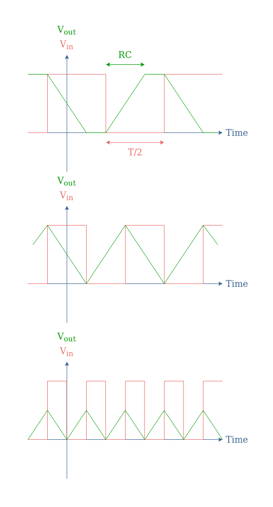
We can illustrate this phenomenon with the following Figure 4 showing the output of the integrator when a square signal of period T is applied at its input.
fig 4: Output of the integrator as a function of the input frequency
In the first case, T/2>RC which makes the output to saturate for a while. In the second case, T/2≅RC is the regime where the integrator performs well the integration operation. Finally, when T/2<RC we can see that the integrator cannot efficiently follow the speed rate.
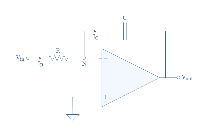
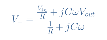
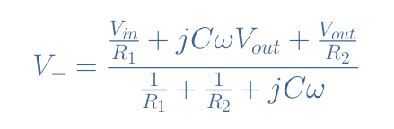
In order to really understand the behavior of the ideal integrator regarding the frequency, we can apply Millman’s theorem to the node N (Figure 1), which gives:
If we suppose the input impedance of the op-amp to be infinite (which is not true but a good approximation), V–=0, and therefore:
eq 2: Transfer function of the ideal integrator
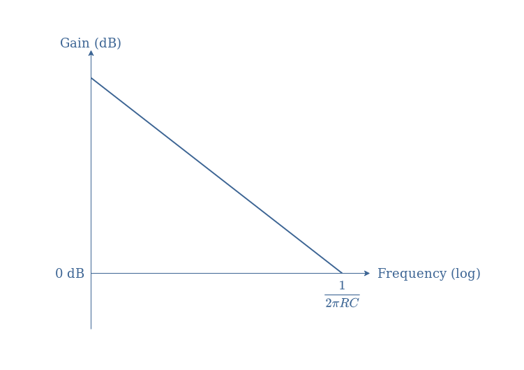
With T being the transfer function of the circuit and x=ω/ω0 (ω0=1/RC). If we convert this data in dB, the gain of the ideal integrator is given by -20log(x), which is a decreasing linear plot G=f(log(x)). The signal phase φ(ω) is here constant and given by the argument of T, since arg(T)=arg(-1)-arg(jx), φ=π-π/2=+π/2.
As a consequence, the Bode diagram of an ideal integrator is given by the following Figure 5:
fig 5: Bode plot of the ideal integrator
Output formula
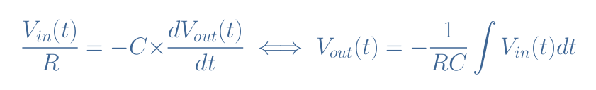
If we suppose the op-amp in Figure 1 to be ideal, the hypothesis i+=i–=0 and V+=V–=0 are verified due to its infinite input impedance. Therefore, the current across the resistor IR is equal to the current across the capacitor IC.
This current can simply be expressed by I(t)=Vin(t)/R when applying Ohm’s law to the input branch, moreover, we can apply Equation 1 in the feedback loop to write a second expression of the same current: I(t)=-C×(dVout(t)/dt).
Finally, when equalizing the two expressions of I(t), we get the output formula of the integrator op-amp shown in Equation 3. This formula highlights the fact that the output is proportional to the integral of the input signal.
eq 3: Output formula of the integrator op-amp
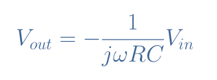
Equation 3 can actually be simplified by using the complex notation:
eq 4: Complex output formula of the integrator op-amp
Limitations
As we highlighted in the previous section, the circuit presented in Figure 1 presents the inconvenience of behaving like a comparator when a DC input is applied to it. This could not be a problem if the amplifiers are considered ideal supplied with signals without any DC component such as pure sine waveforms for example.
However, in real circuits, op-amps always present an off-set voltage (refer to the corresponding tutorial) which would make the configuration in Figure 1 always saturate, even without any input signal.
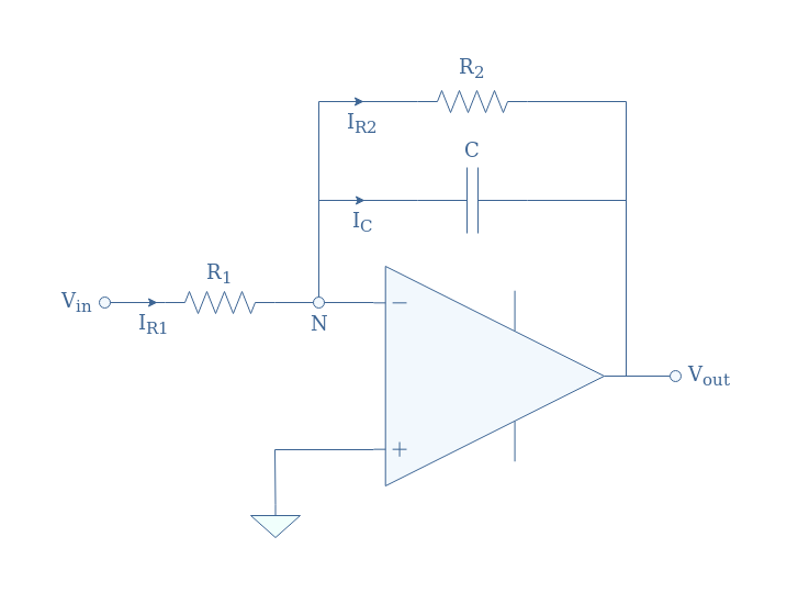
In order to solve this undesirable behavior, a resistor can be added in parallel with the capacitor to obtain the so-called pseudo-integrator circuit:
fig 6: Pseudo-integrator circuit representation
In the DC regime, when the capacitor C acts as an open circuit, the resistor R2 provides a feedback path allowing the circuit to behave as an inverting amplifier with a closed-loop gain -R2/R1.
At high frequencies, the capacitor shortens the resistor R2 making the circuit tend to behave as an inverting voltage buffer.
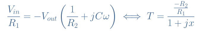
So why is this circuit called a “pseudo-integrator”? In order to answer that question, let’s again apply Millman’s theorem to node N in Figure 6:
Due to the same hypothesis as previously mentioned, V–=0, which leads to the expression of the transfer function of the real integrator:
eq 4: Transfer function of the real integrator
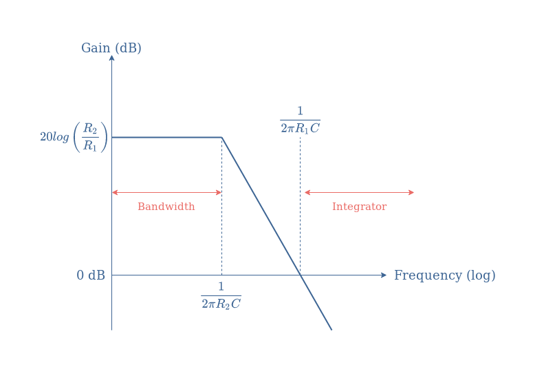
The parameter “x” is here given by ω/ω0 with ω0=1/R2C playing the role of the cutoff frequency at -3 dB. For frequencies from DC up to ω0, T can be approximated to -R2/R1, hence the gain being given by 20log(R2/R1). At ω0 and above, the gain experiences a -20 dB/decade loss, similarly to the ideal integrator, the gain is equal to 0 dB for ω=1/R1C.
As for the phase of the signal, it varies from π when the gain is constant to π/2 when the frequency tends to infinite values.
With this information, the asymptotic Bode plot of the real integrator can be given in Figure 7:
fig 7: Bode plot of the real integrator
As a consequence, we can say that a real integrator behaves as a low pass filter with a cutoff frequency depending on the capacitor and resistor present in the feedback loop.
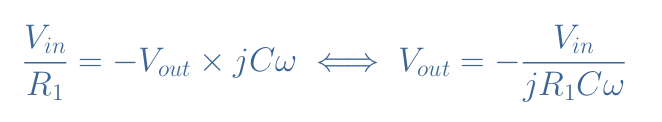
From the first part of Equation 4, we can see that when the frequency is very high, the equality between Vin and Vout is reduced to:
This equation is similar to the ideal integrator transfer function given by Equation 4 pseudo-integrator circuit and we can conclude that the real integrator circuit is a good approximation of an ideal integrator for frequencies significantly higher than its cutoff frequency.
Conclusion
The mathematical operation “integration” can be realized by an electronic circuit called an integrator, which is based on an operational amplifier working in inverting configuration with a reactive component in its feedback loop.
We highlight in the first section how the frequency behavior of the capacitor modifies the entire functioning of the circuit by alternatively opening and closing the feedback loop when variations of the input signal are present.
Due to the charging and discharging time of the capacitor, we show that depending on the frequency of the input signal, the circuit follows more or less the variations. When the frequency is too low, the output tends to reach the saturation level which is not part of the integration operation. On the other hand, when the frequency increases too much, the gain of the output drastically decreases by 20 dB/decade.
The ideal circuit presented in the first section cannot practically be designed due to its tendency to saturate any DC component present in the input signal. To solve this behavior, an extra parallel resistor is added in the feedback loop for real integrators. As a consequence, the circuit acts as a low-pass filter and start to properly integrate the signal only above a certain frequency given by the product of the capacitor and resistance in the input branch.
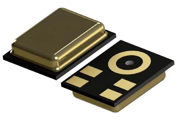
The MP23DB01HP is an ultra-compact, low-power, omnidirectional, digital MEMS microphone built with a capacitive sensing element and an IC interface with stereo operation capability.
The sensing element, capable of detecting acoustic waves, is manufactured using a specialized silicon micromachining process dedicated to producing audio sensors.
The IC interface is manufactured using a CMOS process that allows designing a dedicated circuit able to provide a digital signal externally in PDM format.
PDM single-bit output with option for stereo configuration
RHLGA package
Bottom-port design
SMD-compliant
EMI-shielded
ECOPACK, RoHS and “Green” compliant
The MP23DB01HP offers multiple performance modes (power-down, low-power and performance mode) enabled by different clock frequency ranges. The device has a very high AOP in performance mode, sensitivity range of ±1 dB and high SNR for all operative modes.
The MP23DB01HP is available in a bottom-port, SMD-compliant, EMI-shielded package and is guaranteed to operate over an extended temperature range from -40 °C to +85 °C.
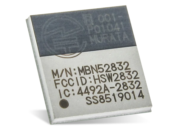
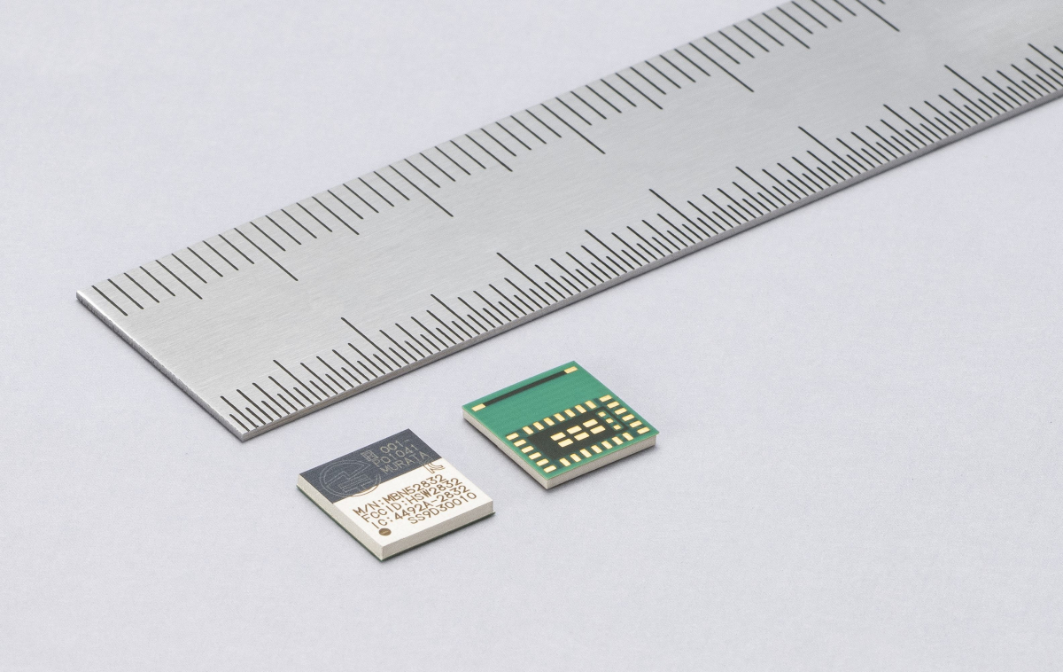
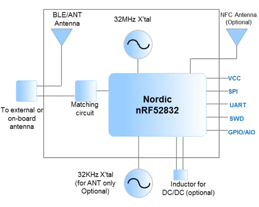
Murata Electronics MBN52832 BLUETOOTH® Low Energy (BLE) 5.0 Module (WSM-BL241-ADA-008) enables ultra-low power connectivity for data communication. The MBN52832 BLE Module integrates Nordic Bluetooth Low Energy IC, RF front end, and crystal into a very small form factor. The built-in arm cortex M4 core with 64KB RAM and 512KB flash provides a high-performance engine and rich interface for a variety of IoT applications. The IoT applications include sensor network, device control and more. This RF certified module can significantly reduce the system designer’s burden and help to reduce the time-to-market. The MBN52832 Module is an ideal solution for smart devices, medical and healthcare, and Machine to Machine (M2M) applications.
Shielded Ultra Small Bluetooth 5.0 LE Module
2.4GHz BLE, ANT and NFC tag MCU Module
Chipset: Nordic (nRF52832)
Processor: ARM Cortex-M4
FCC/IC Certified
Features
Bluetooth v5
Higher throughput
Increased broadcast capacity
Improved channel co-existence algorithm (SCA)
ANT, NFC Tag
Nordic nRF52832 Bluetooth Smart
Built-in Arm Cortex M4 core with 64KB RAM and 512KB flash
Bluetooth/ANT Antenna Configuration:
On-board PCB antenna
Supports external antenna from pin pad
Maximum transmit power: +4dBm @ antenna port (LDO Mode)
Receive sensitivity: -93dBm @ 1Mbps (LDO Mode)
Power consumption
TX: 7mA @ 3.5dBm (DC-DC Mode)
RX: 6mA (DC-DC Mode)
Host interface: UART, SPI
Other interfaces: 20 GPIO, 5 ADC, UART, SPI (master and slave), I2C, PWM and Debug SWD
Panasonic expands its sensor technology offering to include the laser type particulate matter sensor
Panasonic’s laser type PM sensor is an addition to its already broad range of specialty sensor solutions. It is comprised of an on-board microprocessor, micro-fan, and laser diode. This sensor has been programmed so that the fan will operate based on the amount of particle dust surrounding the laser diode so that overall lifespan or usefulness of the sensor can be extended much longer than its average commercially available equivalent.
Featuring a very small footprint of 37 mm x 37 mm x 12 mm, the Panasonic laser type PM sensor can be used to detect a wide variety of PM including, but not limited to, dust, fly ash, soot, smoke, aerosols, fumes, mists and condensing vapors, solid fuels, construction materials, cooking/smoking of plant matter, fireplaces and furnaces, house/forest fires, waste incineration, and much more.
Specifications
5V (±10%) power supply voltage
Below 100mA of current consumption
I2C and UART external interface
0.3μm minimum detectable particle
Response time 1sec
Time to first reading 8sec
Small footprint of 37mm x 37mm x 12mm
Weighs about 13g
Features and Benefits
Panasonic’s on-board microprocessor makes it unnecessary for customers to design their own
The inclusion of a micro-fan is more efficient than simply having a heating element to draw air into the sensor
RoHS And REACH compliant
Panasonic’s PM sensor provides more accurate light scattering performance using a laser diode than light-emitting diodes (LEDs)
Panasonic’s proprietary algorithm controls fan and laser diode efficiency for prolonged product life
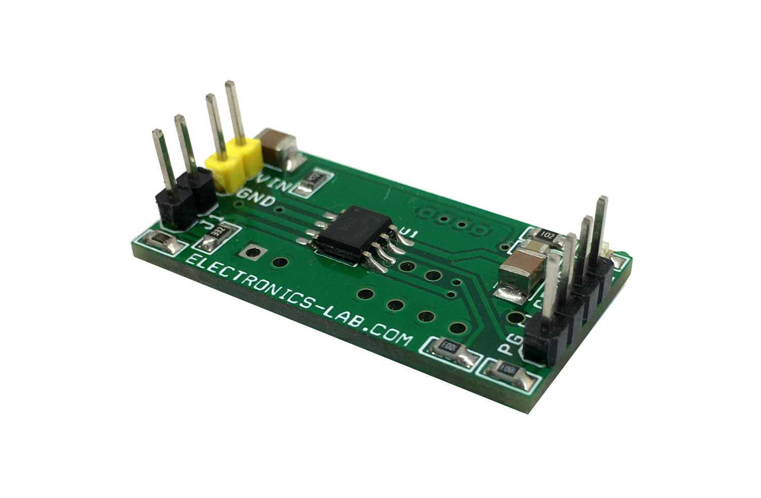
The Over-current limit load switch project presented here provides full protection to devices and loads from access load conditions. The default current limit is set to 1 Amp, however, this load limit is adjustable from 0.4A to 2A with the help of R4 ISET resistor. When an overload condition occurs circuit responds to that overload condition that lasts longer than a fixed blanking period by turning off the load, followed by a retry after the auto-restart time, auto-retry time is 127.5ms. Flag output is pulled up with R1 and the board provides active low output in a fault condition, normally Flag output is high. Power good output is also pulled up and it’s an open-drain output to indicate that the output voltage has reached 90% of the input voltage. The input range of this circuit is 5V to 24V DC. The load can be activated or deactivated with low-voltage logic compatible on Pin4, jumper J1 is provided to activate or deactivate the output. Close the jumper J1 to activate the output load.
Aside from the security issues revolving around face recognition, its value as a technology still remains intact, as its is used everyday by most people, either to unlock their phones or in other apps and as utensile in our environment, wether to find missing people or even helping secure transactions. Its potential still remains a bit untapped, as it usually is highly demanding when it comes to computer resources, making it difficult for a lot of people to get their hands on the technology and develop projects with it. This is where the new MCU-based face recognition solution from NXP comes in handy!
The solution NXP came up with is a cost-effective implementation of offline face recognition, including production-ready hardware and software that will enable you to easily integrate face and motion recognition capabilities into a wide range of IoT products, being ideal for OEM’s who want a “fully integrated, self-contained, software and hardware platform”. The solution is based on the i.MX RT106F MCU and includes te NXP face and emotion recognition run-time library, a group of pre-integrated machine learning algorithms, along with the necessary peripheral drivers to go along with it, such as camera, memories and other optional connectivity features. It comes in a really small form factor, that can easily be integrated into many IoT environments easily. Besides the small form factor, its well documented, fully tested and supported software promise to accelerate the time to market and reduce the complexity of your next face recognition projects.
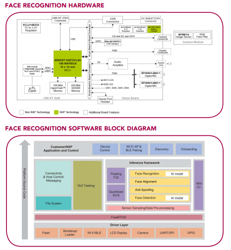
Regarding its specs, the SLN-VIZN-IOT development kit packs:
i.MX RT106F Vision crossover processor (600MHz ARM Cortex-M7 MCU with complete voice solution software)
Connectivity: 802.11 b/g/n Wi-Fi + Bluetooth LE 4.2
Hardware and software block diagrams for the SLN-VIZN-IOT
Besides the aforementioned specs, you have some computer vision functionalities at your disposal, such as face detection, tracking, alignment and recognition, with quantified results. Since the board performs the face recognition without any extra hardware and provides some interesting security features, this may help to give some extra trust to the technology, as it removes the need for an expensive Linux-based implementation and cloud communication.
But where can this board be of use to you? Well, that is the easy part: from smart appliances to industrial, security, and safety devices, there is a wide range of projects where the face recognition on edge just fits. When it comes to price, you would need to spend about $175 to get your hands on one of these development boards, which is not a bad price for what you are getting.
What do you think about this development board? What use would you give to it?