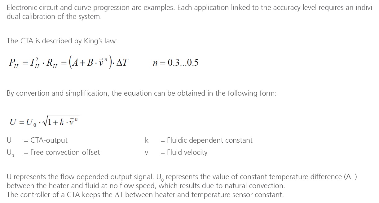
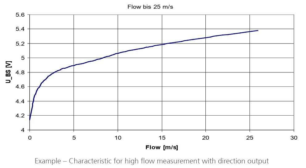
The CTA mode (Constant Temperature Anemometer) consists of a simple feedback circuit for temperature regulation of the heater on the flow sensor and, as flow speed changes the thermal energy loss by the heater changes. By adapting controllers, a constant temperature difference between the heater and the temperature sensor can be achieved. The supplied electrical power, which controls the temperature difference, is a function of the flow speed. The power is converted into a voltage output signal with a bridge circuit and can be easily read out. Knowing the temperature of the medium, the flow rate can be determined from the amount of voltage compensation needed to maintain a constant temperature differential.
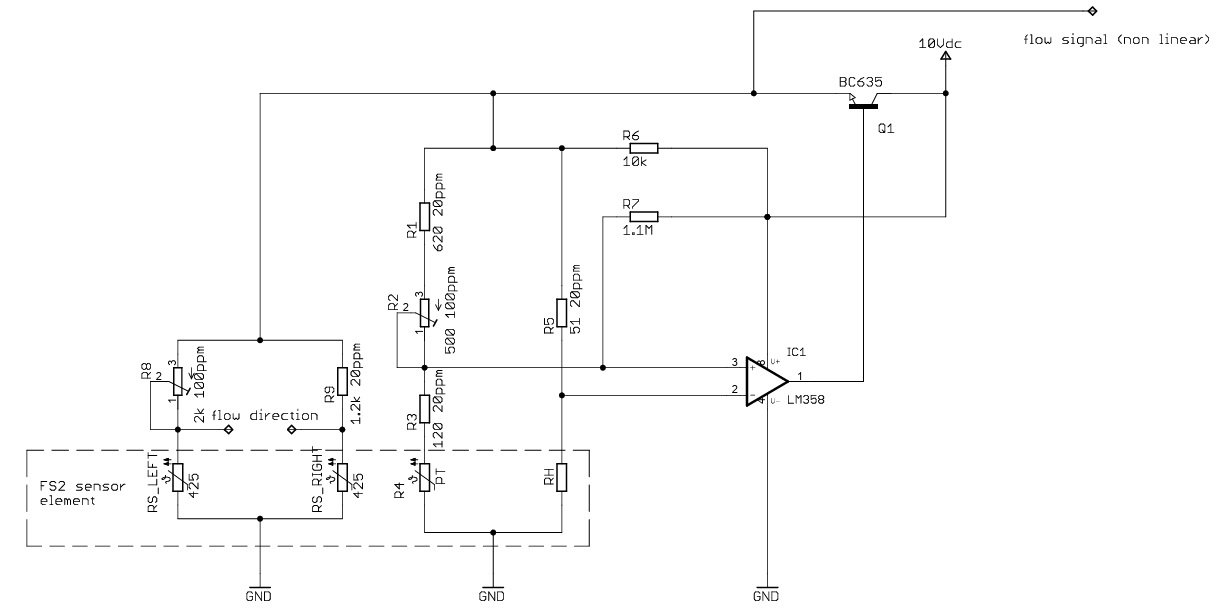
The medium temperature variation is compensated by the temperature sensor on the chip (PT1200). The resistors R1 to R6 can be chosen as shown in the circuit below. The temperature difference (DT) between the heater (RH) and the medium (RS) is set by resistor R4, e.g. DT=30 K for air. The resistor PR2 should be adjustable within ±10 % for calibration. The R8 resistor is placed for the stability of the anemometer circuit. It is important to use high-grade components for accuracy and output stability, all resistors 0.1 to 1%. The below electronic circuits and curve progression are examples. Each application linked to the accuracy level requires an individual calibration of the system.
Credits: Circuit is from IST-AG Application Note (https://www.ist-ag.com/en)
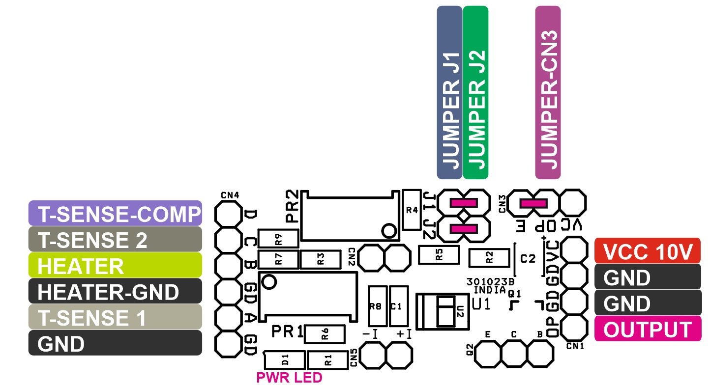
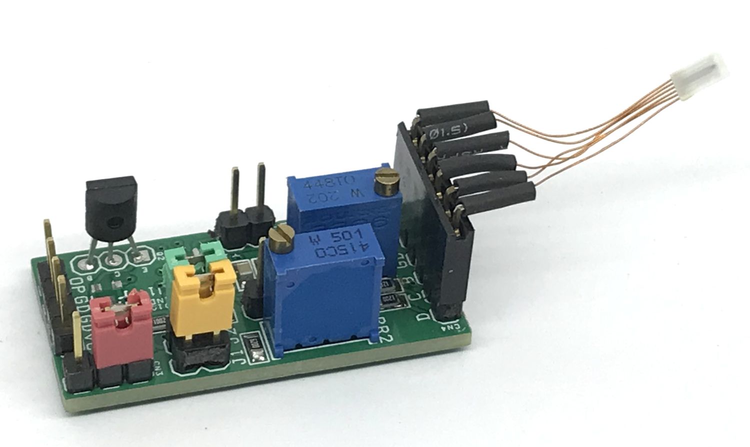
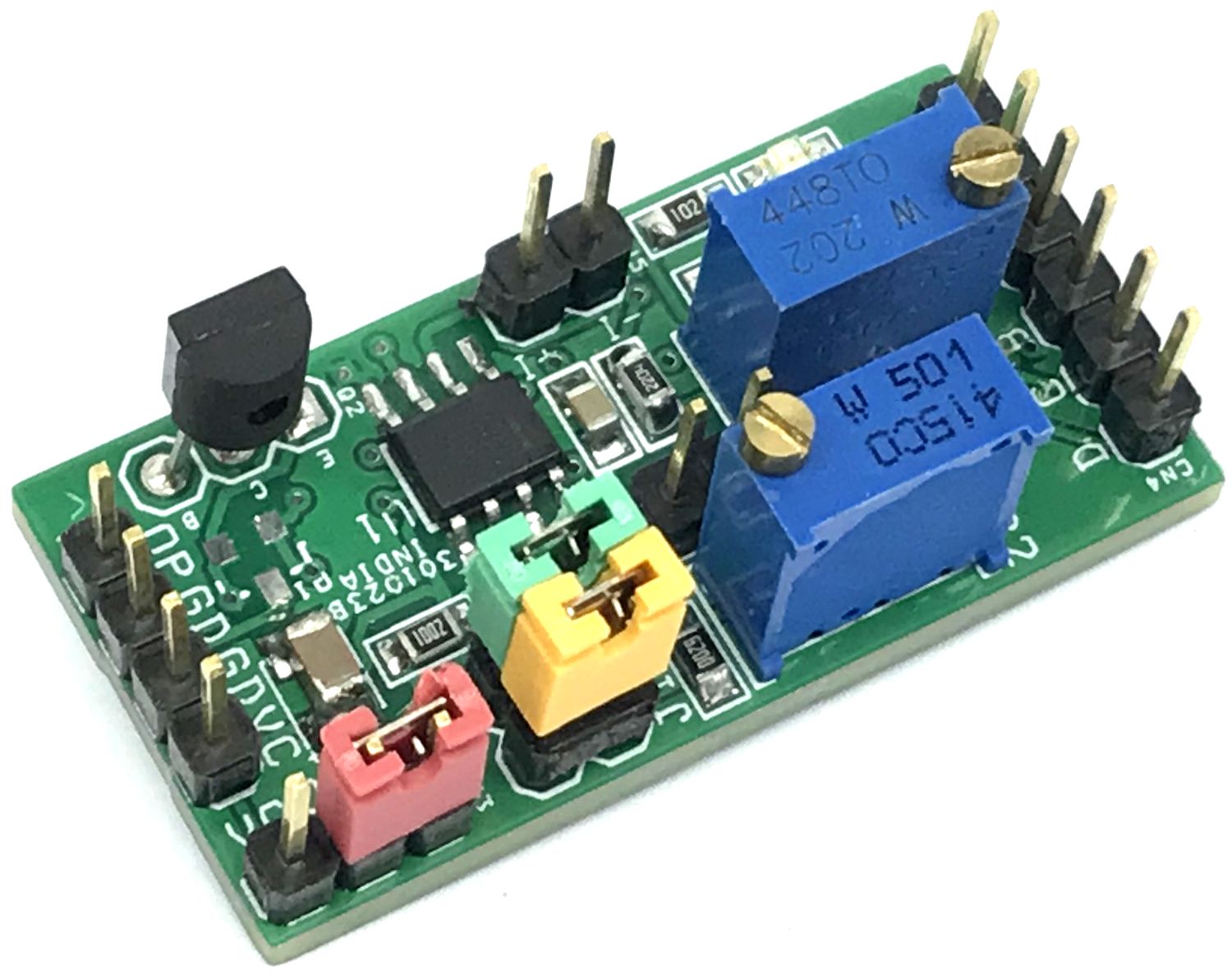
Features
- Power Supply 10V DC @ 80mA
- On Board Power LED
- Trimmer Potentiometers for Calibration
- Header Connector for Sensor
- Header Connector for Power and Output
- PCB Dimensions 36.99 x 18.73 mm
Hot-Film Flow Measurement Principles
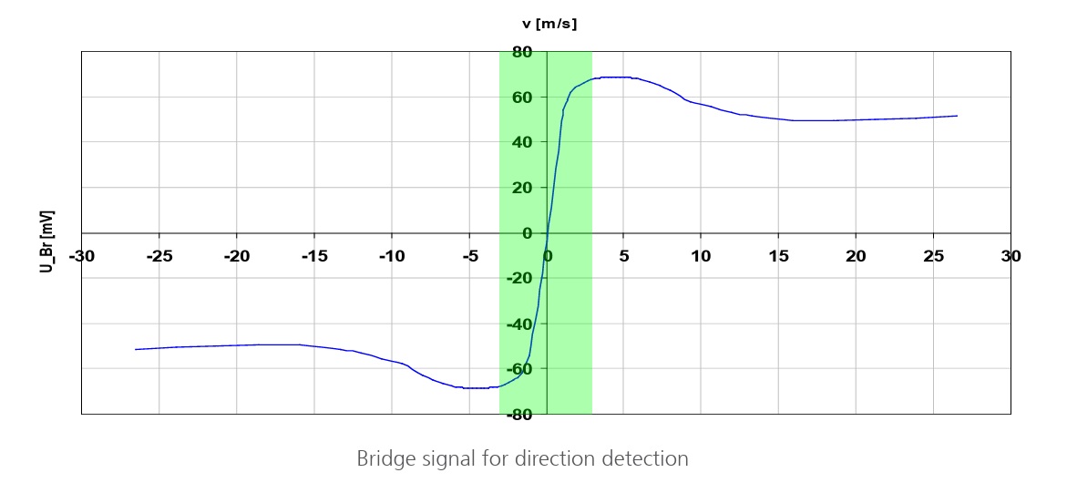
A mass airflow (MAF) sensor converts the amount of air into a voltage signal. Units used are usually kilogram per second (kg/s). For example, airflow mass is a necessary parameter in engine operation in order to determine how much fuel to inject, ignition timing, and when to shift the gears. Used in conjunction with an oxygen sensor, the mass air flow sensor measurement can enable very accurate control of the fuel ratio. There are different types of MAF sensors. The hot-film type sensor is more common. It consists of a heating element (typically a temperature-dependent, low-ohm platinum resistor) and an additional temperature sensor. Flow direction can also be determined with specific sensor configurations. The temperature sensor (Pt in Figure 1) is used as a reference for the heating element to maintain a constant reference to the ambient temperature, which can be provided by an electronic control circuit such as a constant temperature anemometer (CTA) as shown in Figure 1. The voltage needed to heat the element in order to maintain thermal equilibrium with the ambient temperature is proportional to the air mass flow through the sensor. Higher flow increases the cooling of the element, which is compensated by raising the voltage of the heating element. This measuring principle covers large operational ranges with high accuracy and a wide temperature operating range.
The air density can vary, which changes the thermal capacity of the air. The density is a function of the ambient temperature, altitude, and pressure, which makes mass flow meters more appropriate for determining the quantity of the air. Another factor that should be taken in account is the air humidity. An increase in the humidity decreases the air density. This is because the molecule mass of water is less than the molecule mass of air, and for any gas at a
given pressure and temperature, there is a constant number of molecules for a particular volume. This results in a decrease in the gas mass per unit volume. MAF sensors feature a quick response time, small overall package, less sensitivity to mounting and orientation, durability, and lower costs. Care should be taken to prevent contamination of the sensor, which reduces the accuracy. Possible thermocouples between the heating element and the temperature sensor should be taken into account as well.
About the Sensor
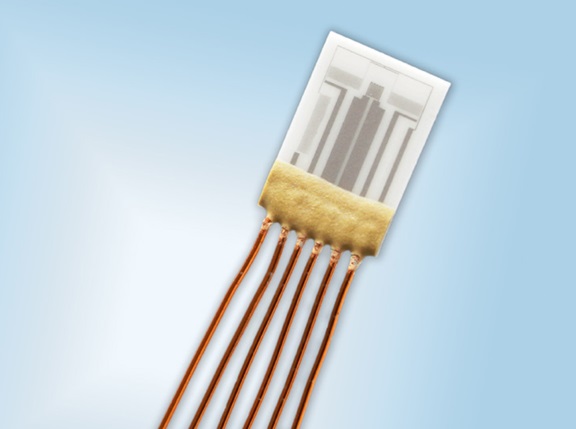
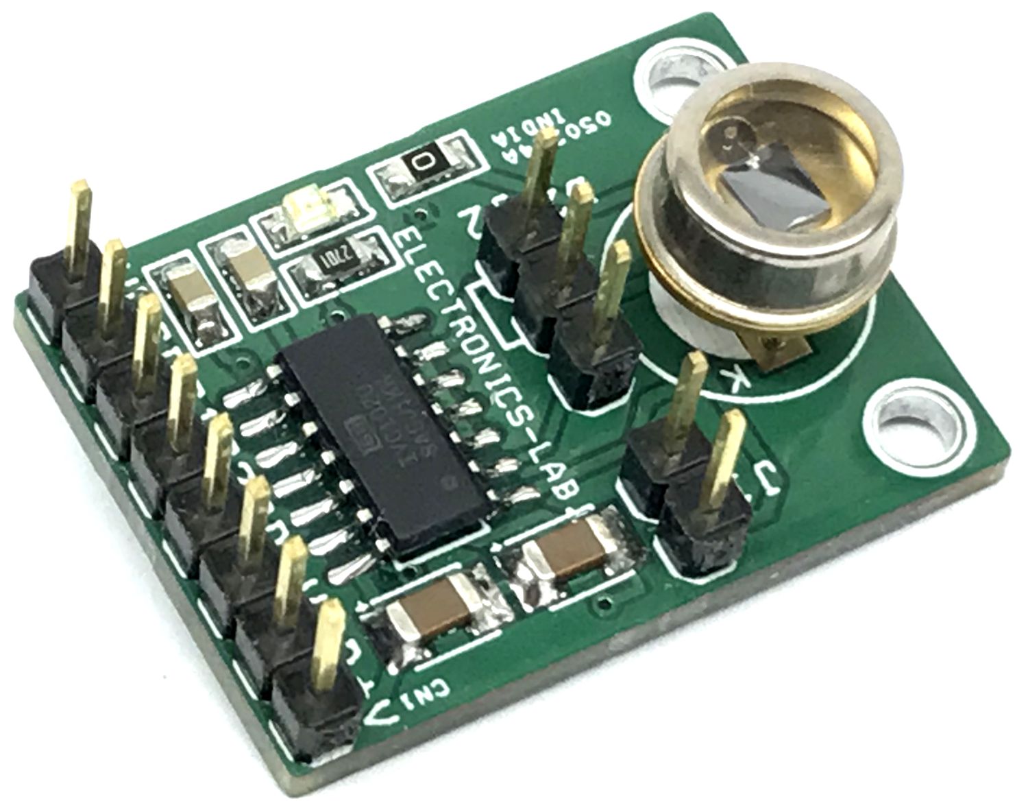
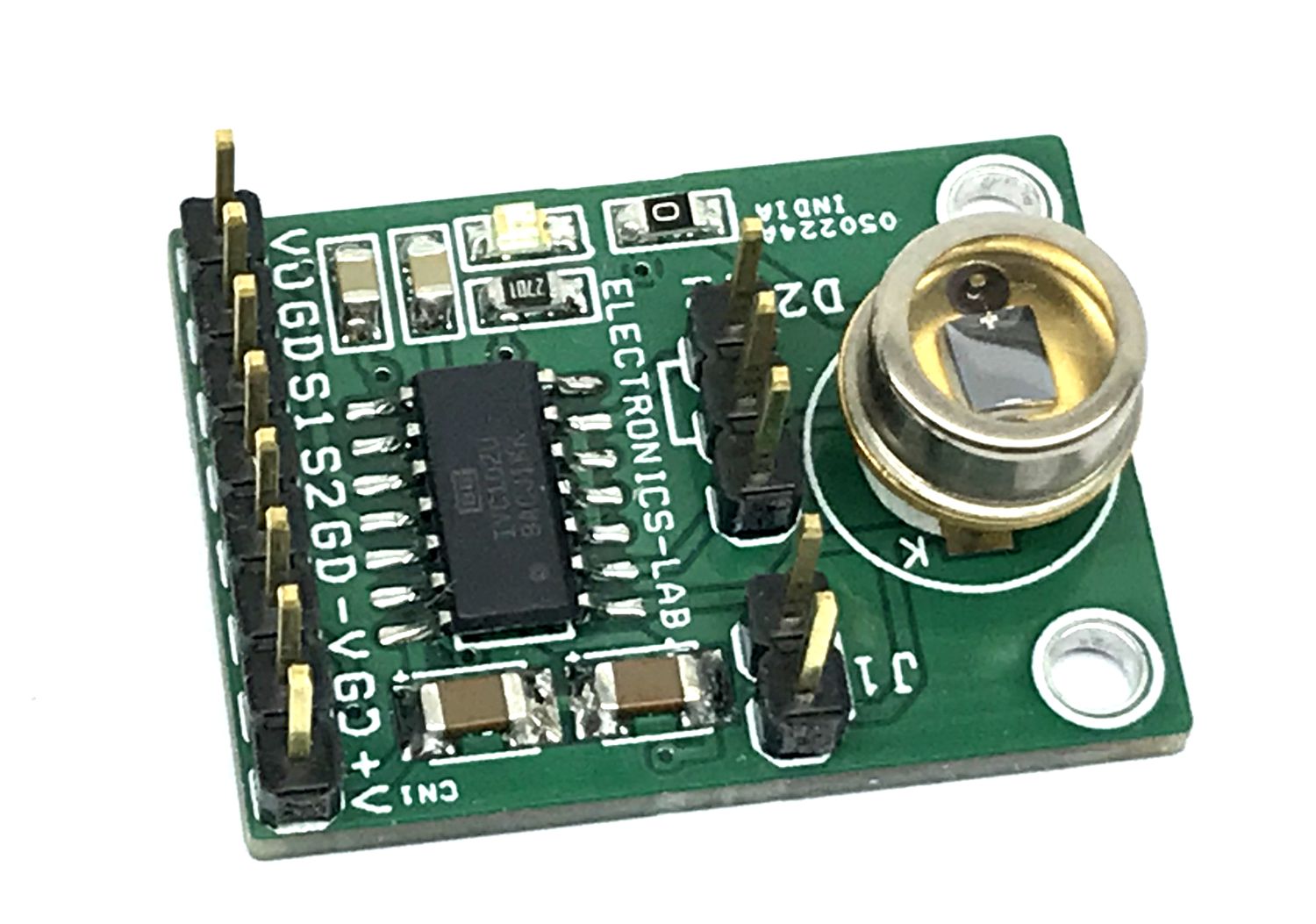
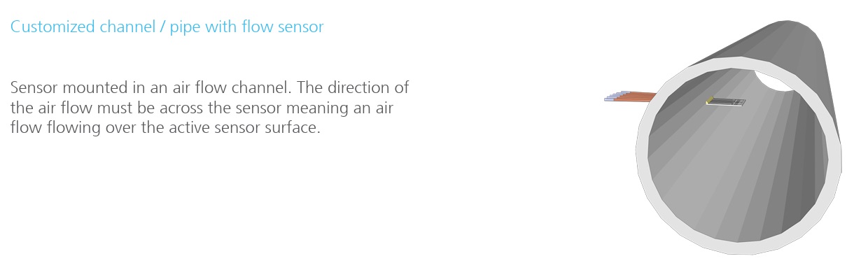
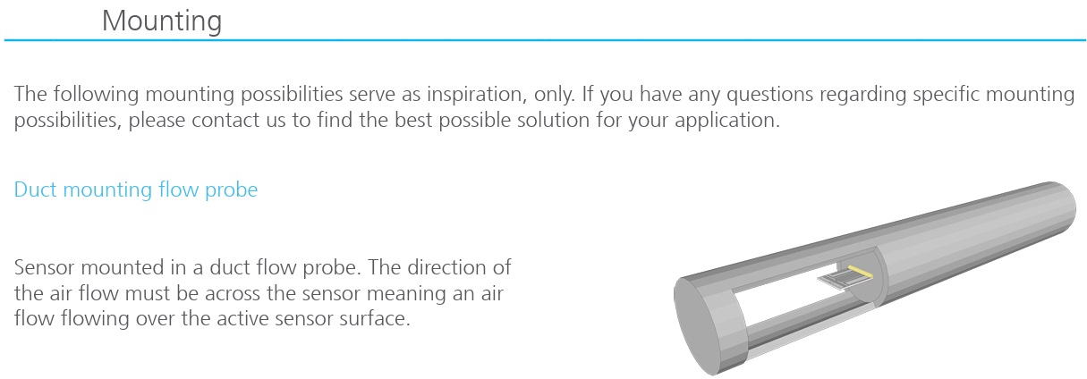
The Innovative Sensor Technology IST AG thin film mass flow sensors were developed to offer solutions for a wide variety of flow applications with considerable advantages. Thermal mass flow modules and measuring systems are well-known devices that are offered in a wide range of applications by a handful of suppliers in the marketplace. Most of these designs are compact, ready-to-use systems with a channel and a passive or active output. These modules are sufficient for many general-purpose applications where component price and size are less significant, but they are not well-suited for price-sensitive and space-limited flow control solutions. The FS2 flow sensor consists of four platinum thin film resistors, is based on a function of the flow speed, and utilizes heat transfer principles to determine the flow velocity. In no flow condition, two resistors are heated up equally. If flow appears, heat is carried from the sensors to the medium, and one of them is cooled more than the other, depending on the flow direction.
If flow increases, so does the amount of heat that is transferred. By knowing the heat transfer, the flow rate can be determined from the amount of voltage compensation needed to maintain a constant temperature differential. The Innovative Sensor Technology IST AG FS2 flow sensors are applicable in gas. They have a wide operating temperature range and flow measuring rate. Flow channels guarantee the best possible adaptation of the sensors to the requirements of your application, whether in terms of dynamic range, response time, or ambient conditions. The FS2 flow sensors are optimal for limited space system integration and can be upgraded into finish-developed systems. Furthermore, customer-specific designs of the chip and housing/channels are possible as well as implementation in customer-defined and supplied housings.
Benefits and Characteristics
The following list showcases the advantages FS2 flow sensors. It is not a list of the sensor’s full range of capabilities and should not be seen as such.
- Detection of flow direction
- Simple signal processing
- Outstanding sensitivity
- Stable platinum technology
- Bare sensor element resists up to +450 °C (customer specific)
- Excellent long-term stability
- Simple calibration
- No moving mechanical parts
- Excellent reproducibility
- Customer-specific sensor available upon request
Application Area
- Among others, the FS2 flow sensor is suitable for, but not limited to, the following application areas:
- Compressed air billing
- HVAC – building automation
- Automotive
- Medical applications
- Device monitoring
- Coolant monitoring
Sensor Data
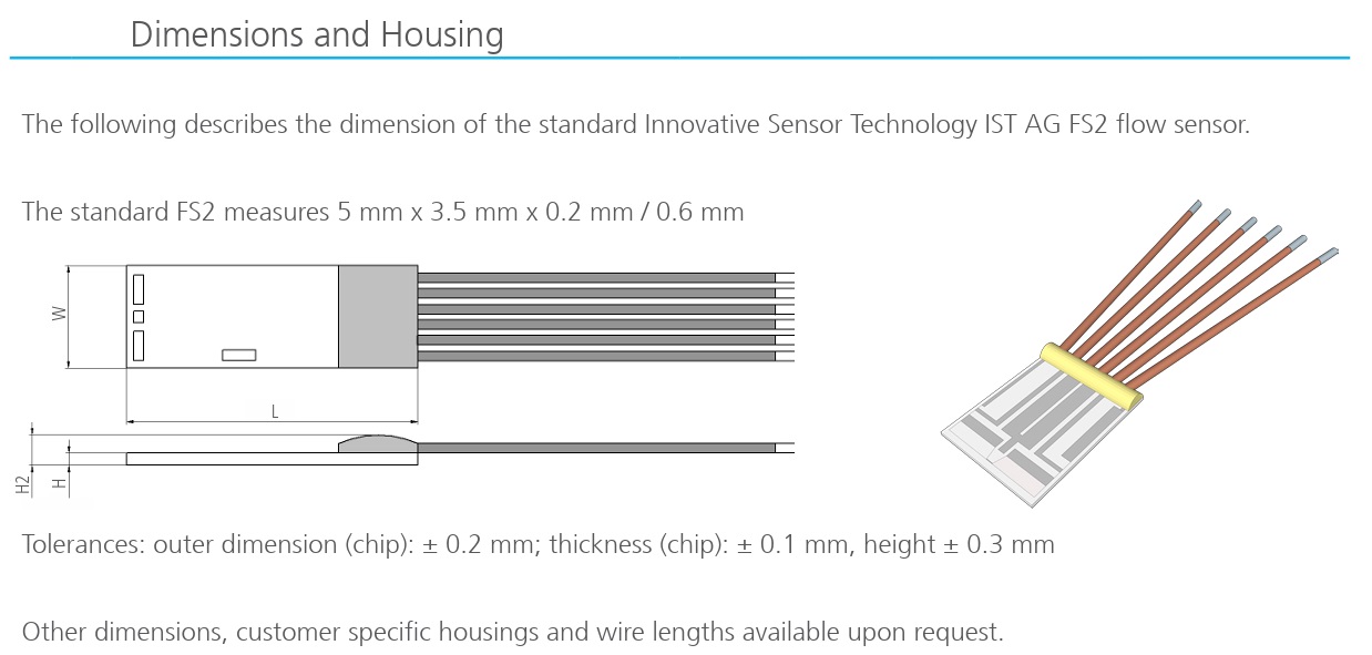
- Dimensions (L x W x H / H2 in mm):0 x 3.5 x 0.20 / 0.60
- Operating measuring range: 0 ml/min to 50 ml/min (half bridge mode), 0 m/s to 1 m/s (half bridge mode) , 0 m/s to 100 m/s (CTA mode) 0 l/min to 5 l/min (CTA mode)
- Minimum operating range: 0 ml/min to 2.5 ml/min
- Response sensitivity:001 m/s (50 μl/min)
- Accuracy: < 2 % of the measured value (dependent on the electronics and calibration)
- Response time t63: < 0.5 s
- Operating temperature range: -20 °C to +150 °C
- Temperature sensitivity: < 0.1 %/K (dependent on the electronics)
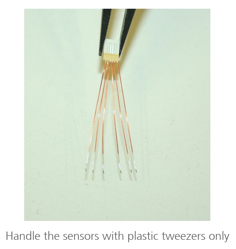
- Connection: Cu-wire, enamelled, Ø 0.2 mm, 25 mm long
- Heater: * RH (25 °C) = 34 Ω ±10 %
- Measuring element: Rs_i (25 °C) = 425 Ω ±10 %
- Reference element: RR (25 °C) = 710 Ω ±10 %
- Voltage range (nominal): 2 V to 5 V (dependent on flow rate)
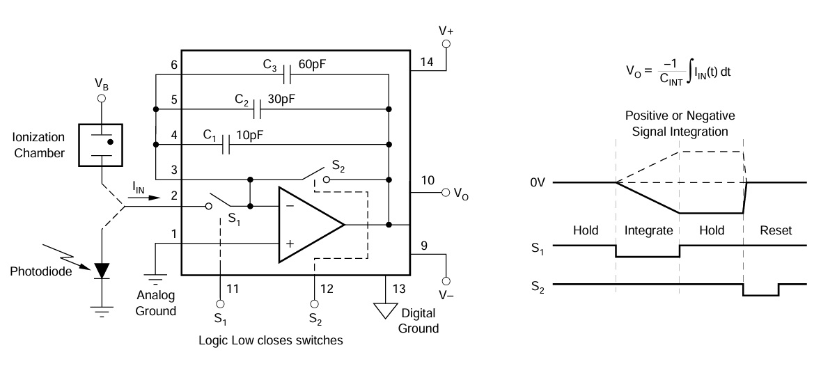
Measurement Principle
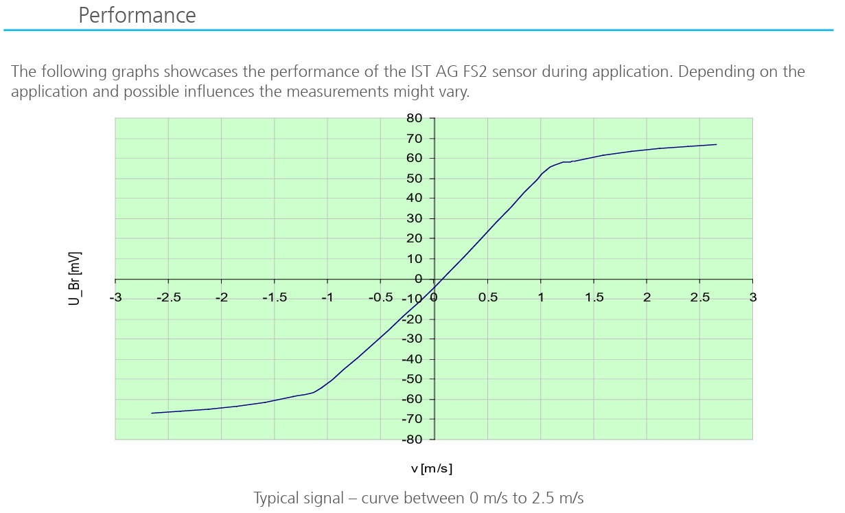
The Innovative Sensor Technology IST AG FS2 flow sensors are based on a variation of the heat transfer coefficient, which is a function of the flow speed. Thermal mass flow sensors utilize heat transfer principles to determine the flow velocity of a medium. Flow speed changes the thermal energy loss by the heater: As a medium passes across the sensor, heat is carried from the sensor to the medium. As flow increases, so does the amount of heat that is transferred, meaning an increase in flow speed results in a higher cooling. This effect leads to a heat transfer coefficient change. Hence, cooling is a function of the mass flow. The Flow Sens FS2 consists of four platinum-thin film resistors. The low ohmic resistance with a small area is used as heater. Two high ohmic resistors on the left- and right-hand side of the heater are used to detect the flow speed and flow direction. A further resistance allows the measurement of the gas temperature. The two resistors close to the heater can be connected in a bridge circuit. This leads in an output signal which is a function of flow speed and direction. In no flow condition, the two resistors are heated up equally. If flow appears, one of them is cooled more than the other, depending on flow direction. The temperature difference can be measured and depends on flow speed and direction. Response and heating up time of this flow Sens is very short due to the small thermal mass. This kind of evaluation allows the measurement of very low flow speeds. In order to detect higher flow velocities, the temperature sensor can be connected in a constant-temperature-an myometer. By adapting controllers, a constant temperature difference between the heater and the temperature sensor can be achieved. This measuring principle is called a Constant Temperature Anemometer (CTA). The supplied electrical power, which controls the temperature difference, is a function of the flow speed. The power is converted into a voltage output signal with a bridge circuit and can be easily read out. Knowing the temperature of the medium, the flow rate can be determined from the amount of voltage compensation needed to maintain a constant temperature differential The range of flow measurements is very wide and can be adjusted to the specific application. Through an electronic circuit, it is possible to increase the temperature of the heater with respect to the temperature of the medium.
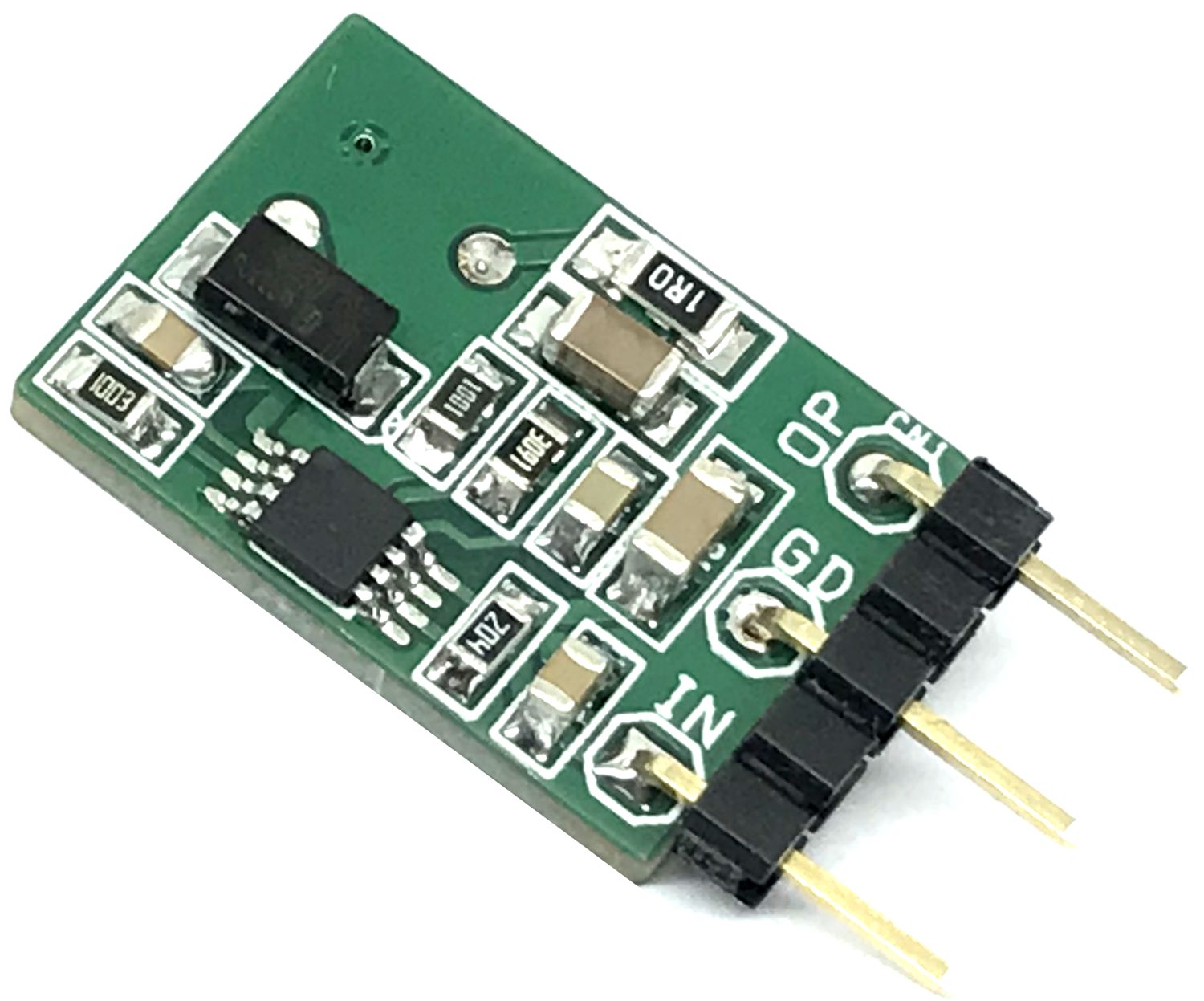
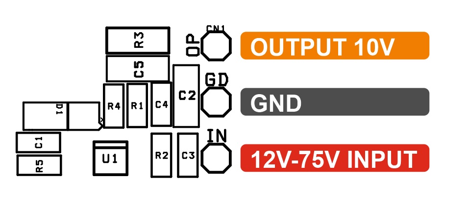
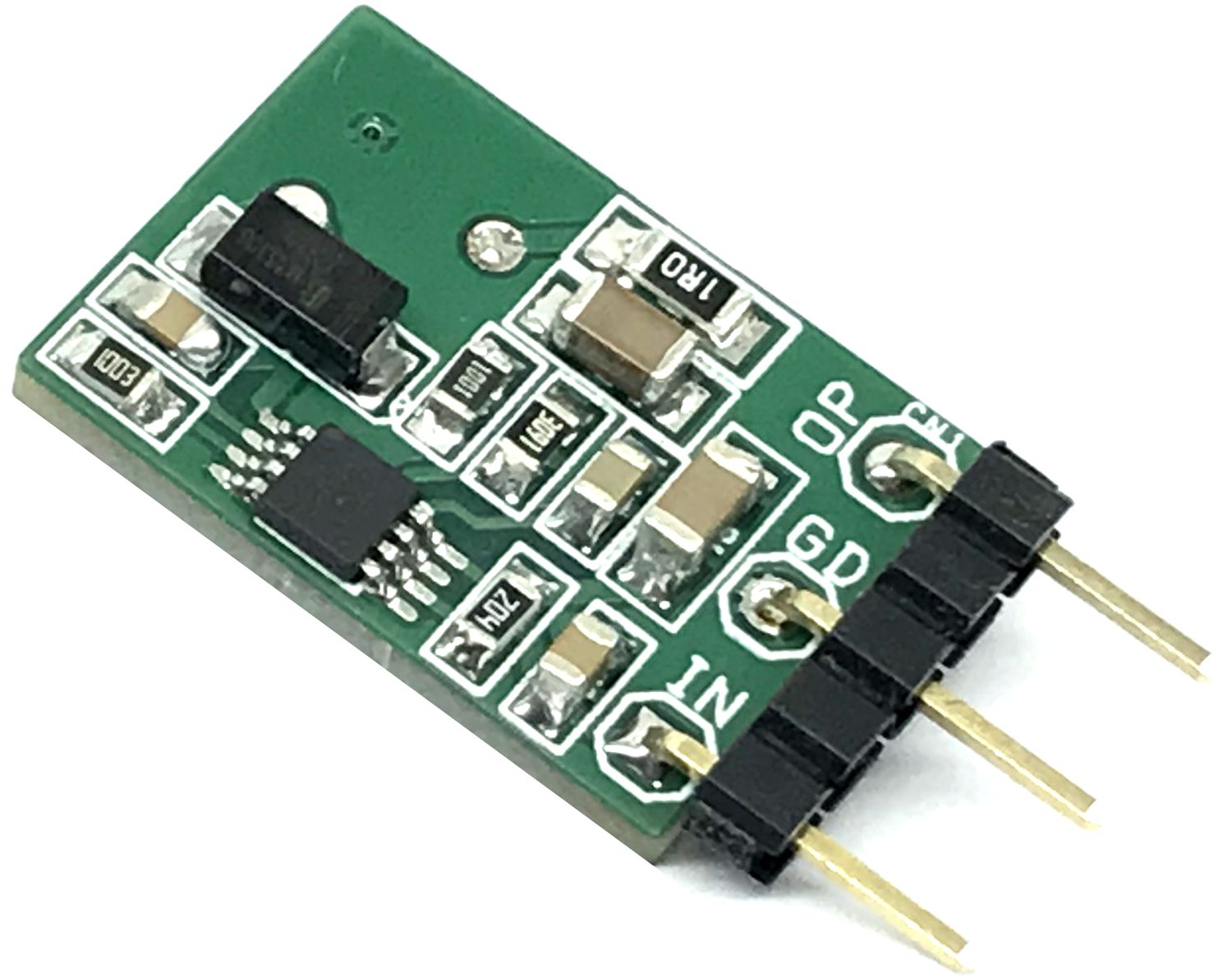
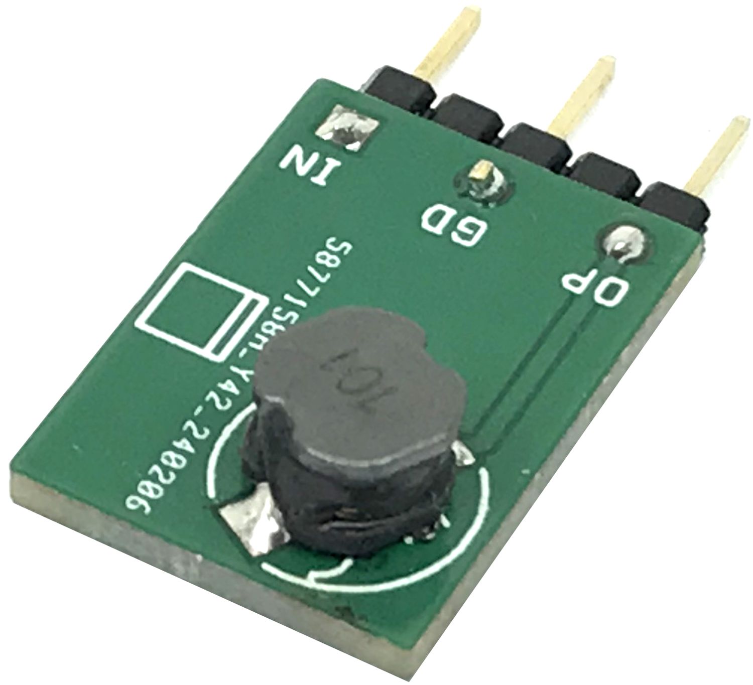
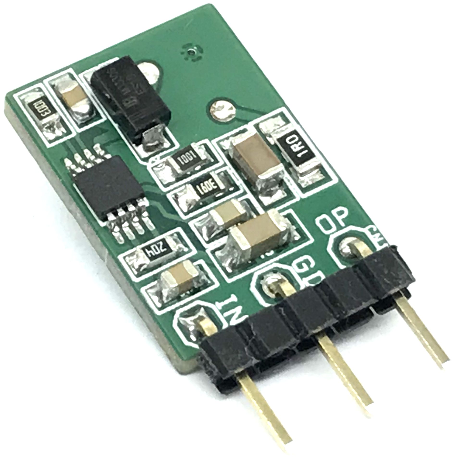
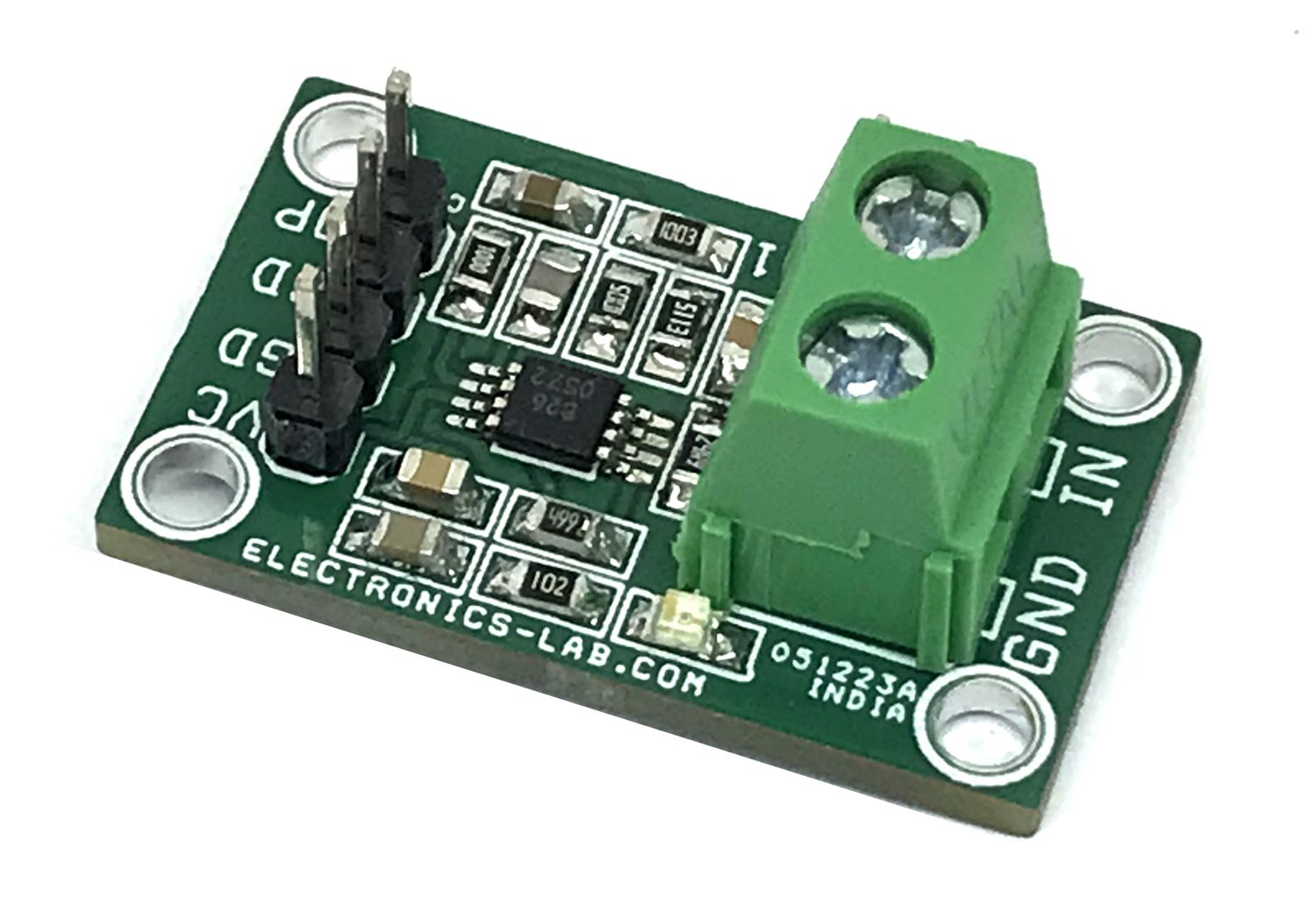
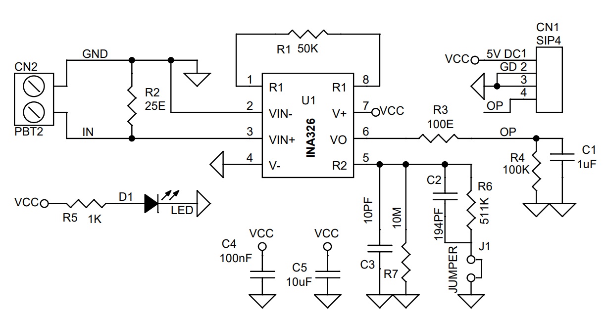
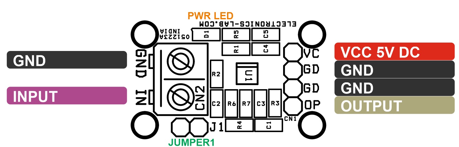
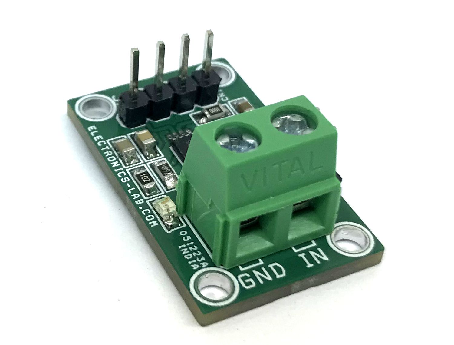
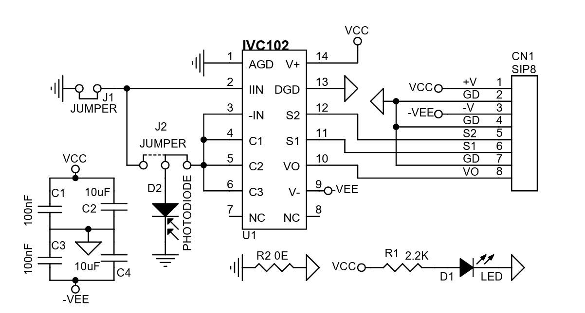
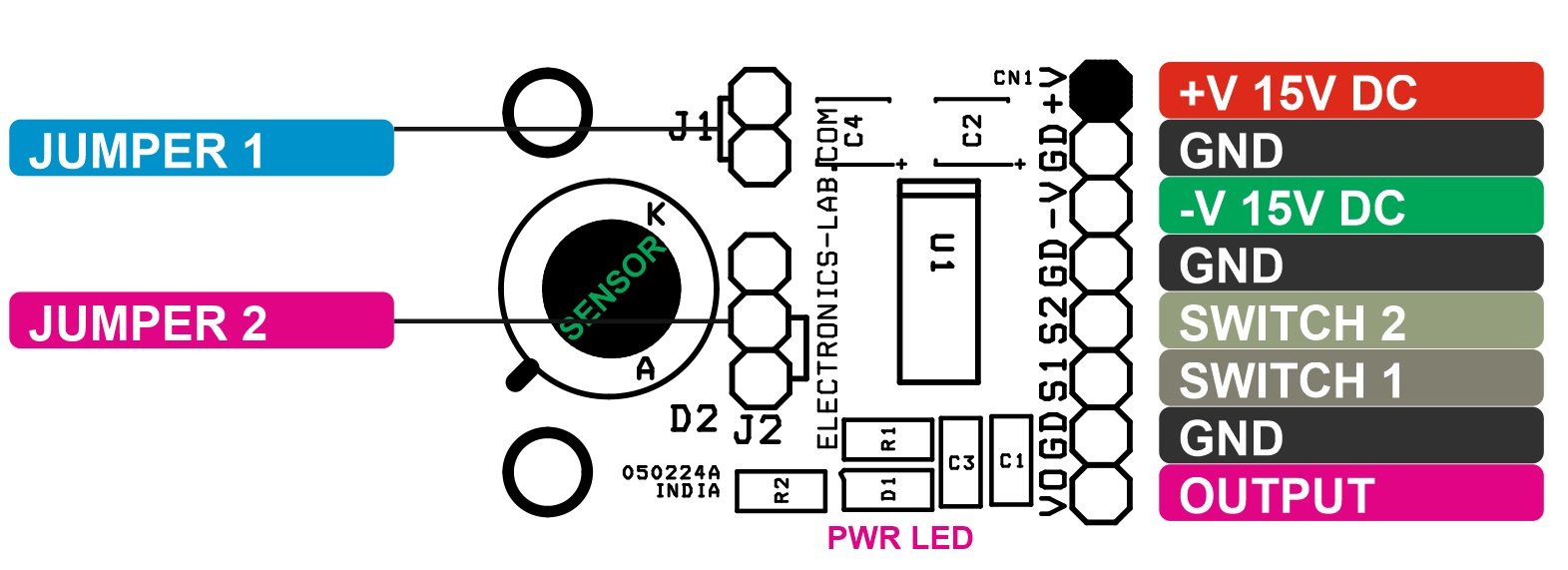
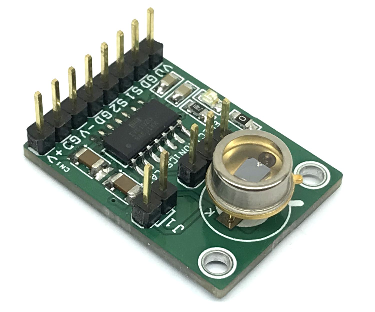
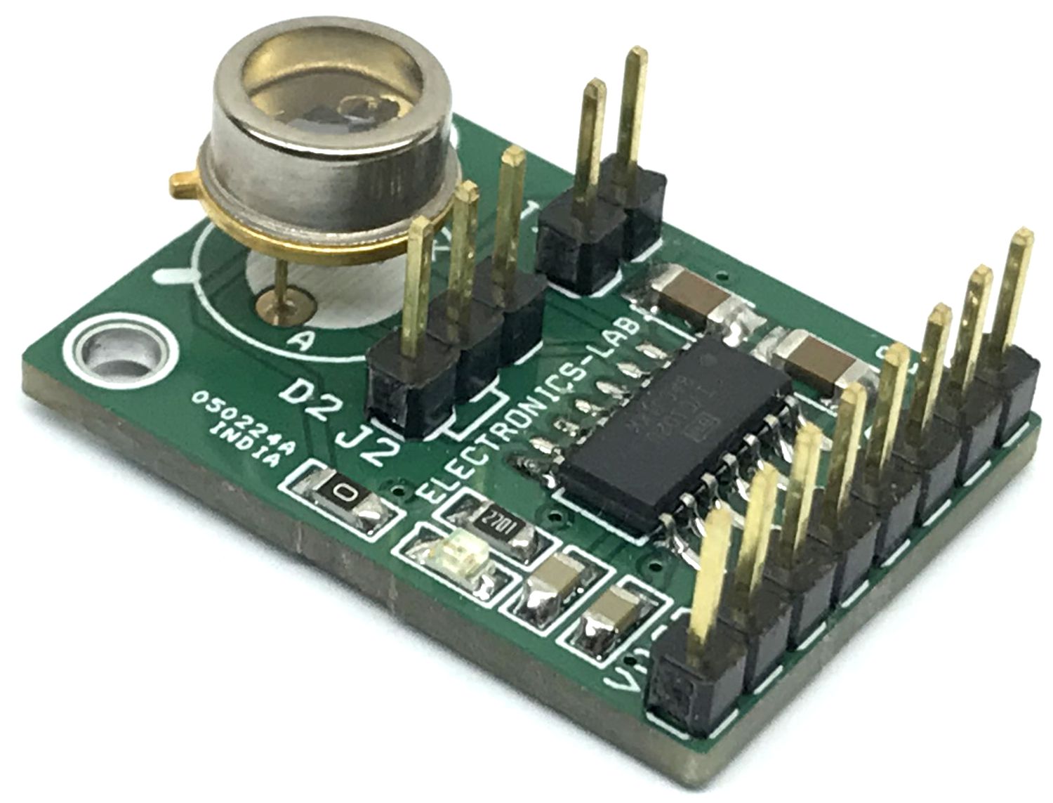
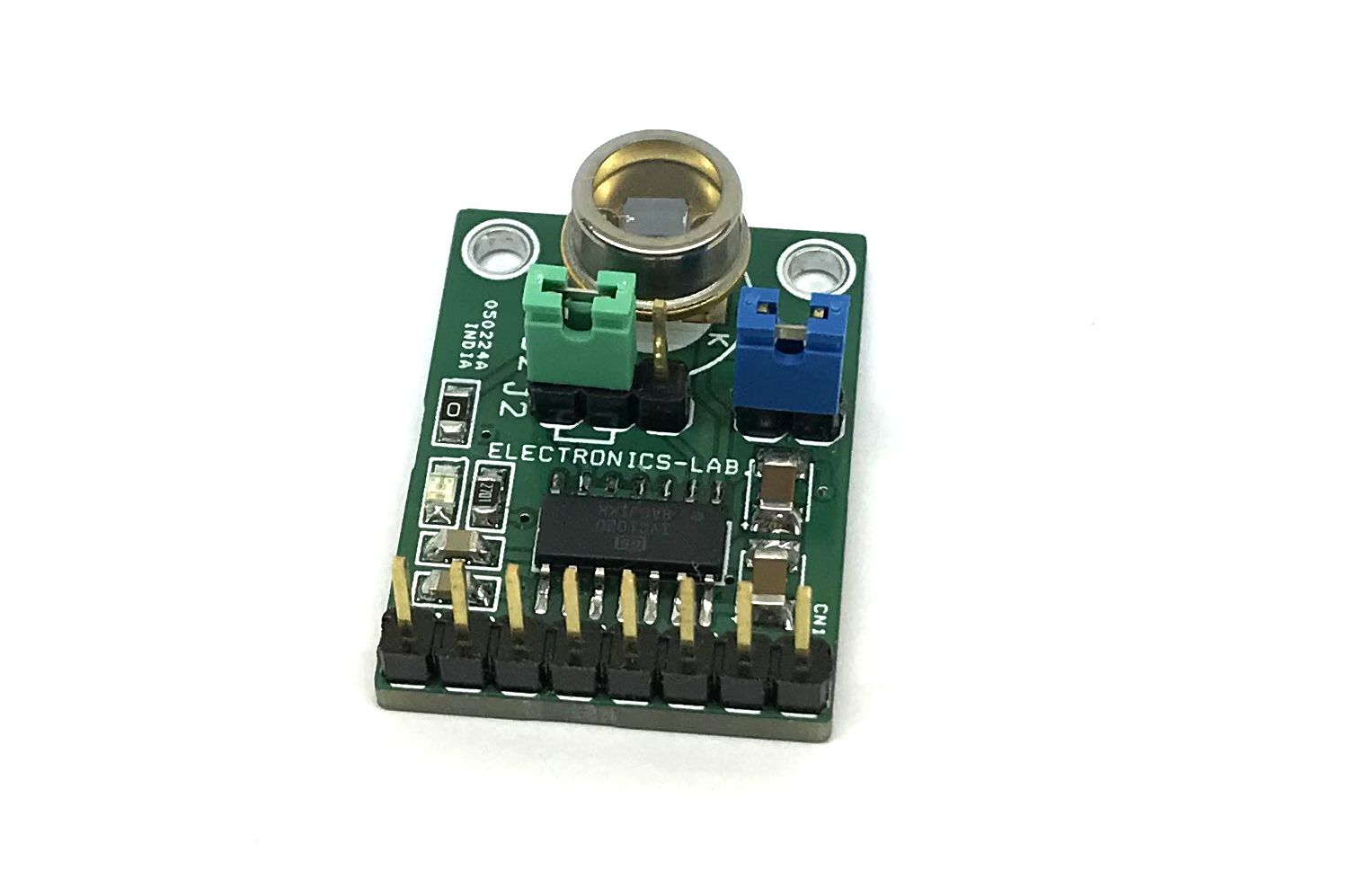
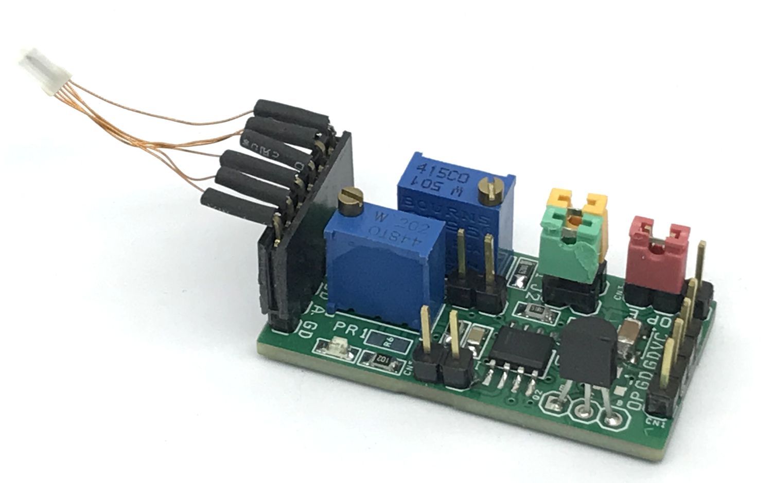
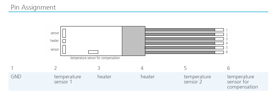
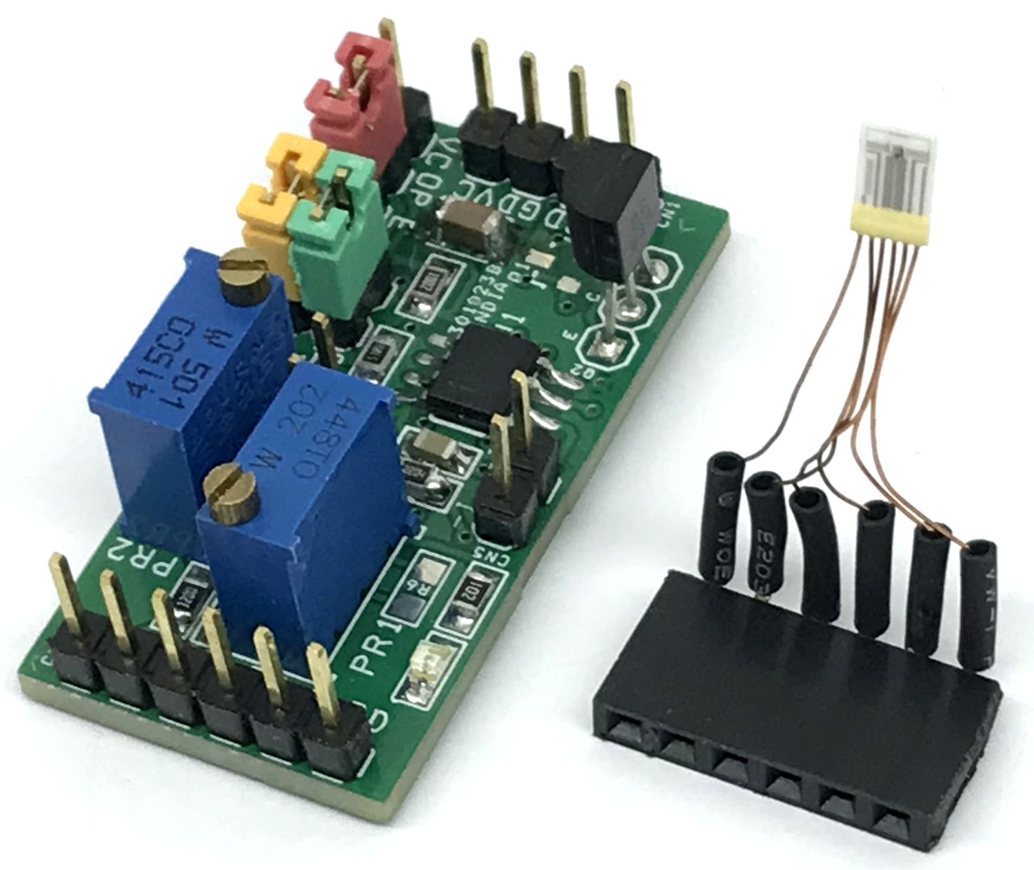
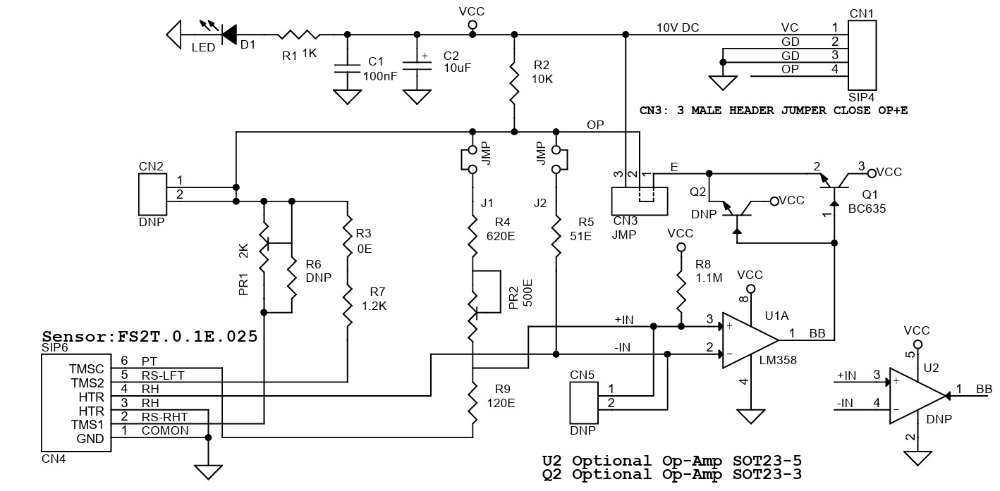
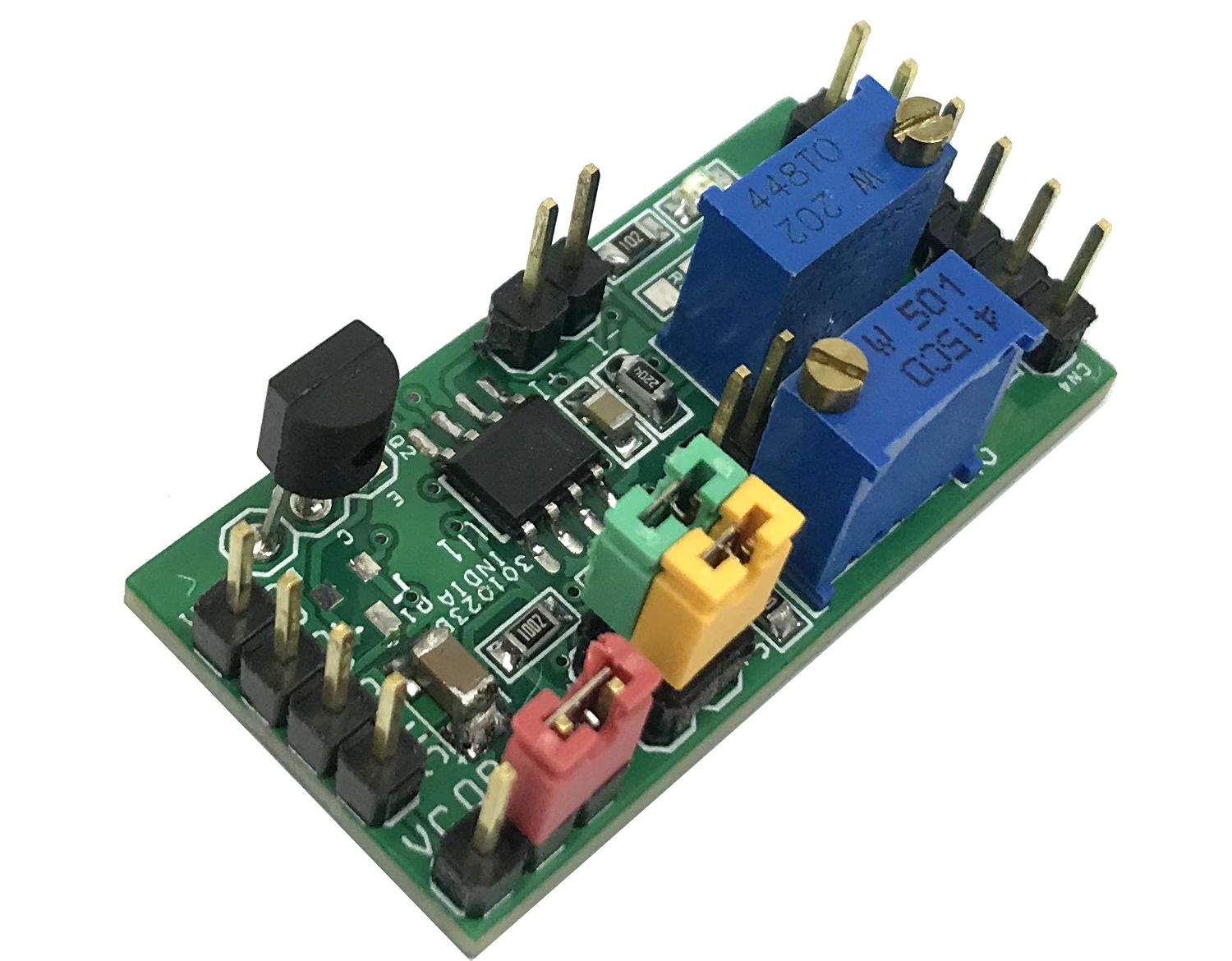
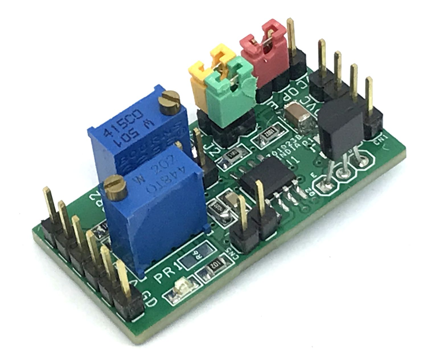
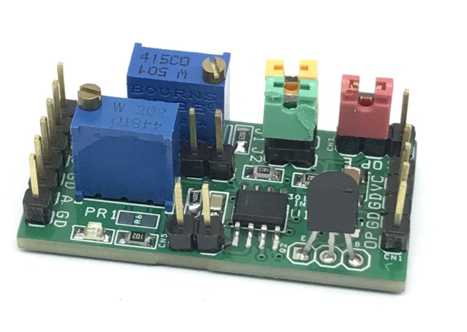
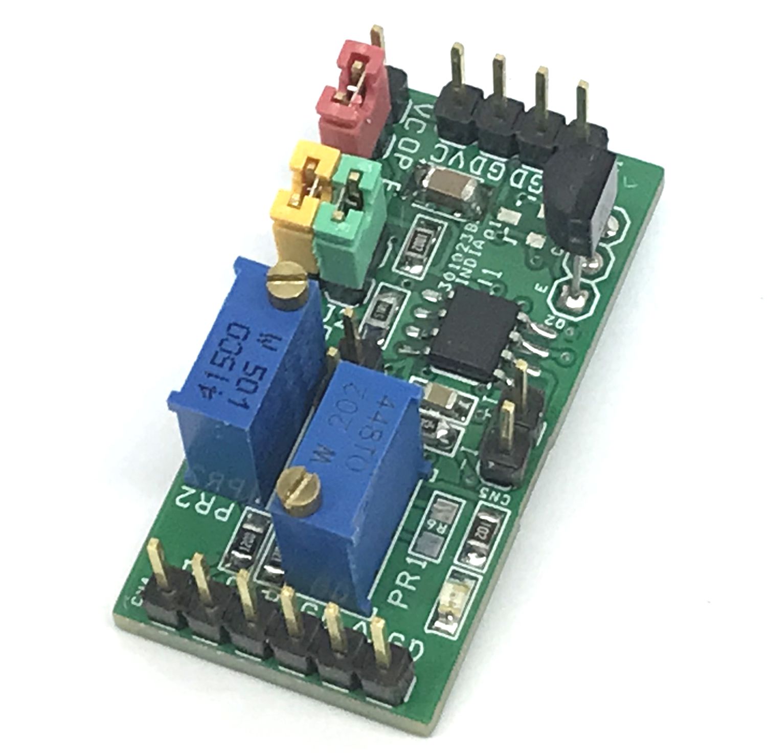
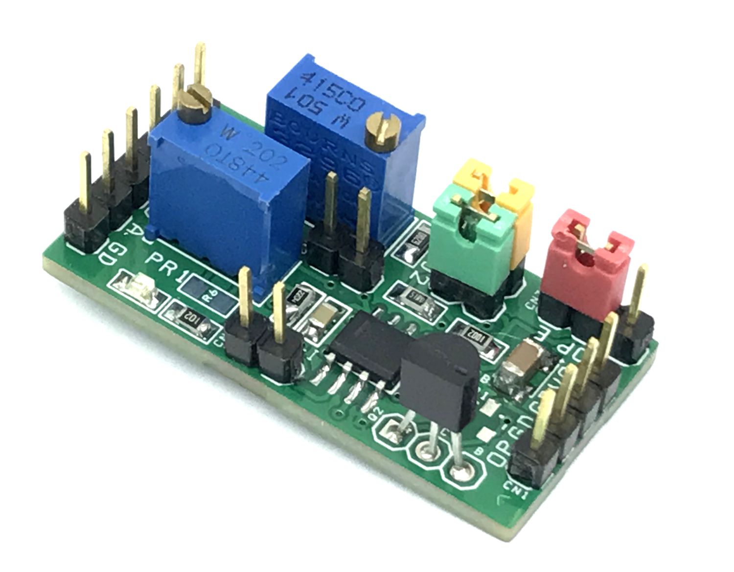
Connections
- CN1: Pin 1 = VCC 10V DC, Pin 2 GND, Pin 3 = GND, Pin 4 = Output
- CN2: Do Note Install
- CN3: Jumper Connect Between OP and E
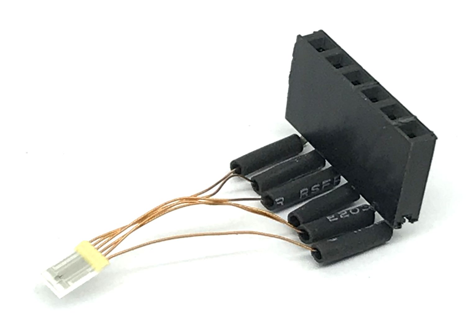
- CN4: Sensor Pin 1 = PT, Pin 2 = RS-LEFT, Pin 3 = RH(Heater), Pin 4 = RH(Header), Pin 5 = RS Right, Pin 6 = Common (GND)
- CN5: Testing Points for Sensor
- J1: Jumper Closed
- J2: Jumper Closed
- D1: Power LED
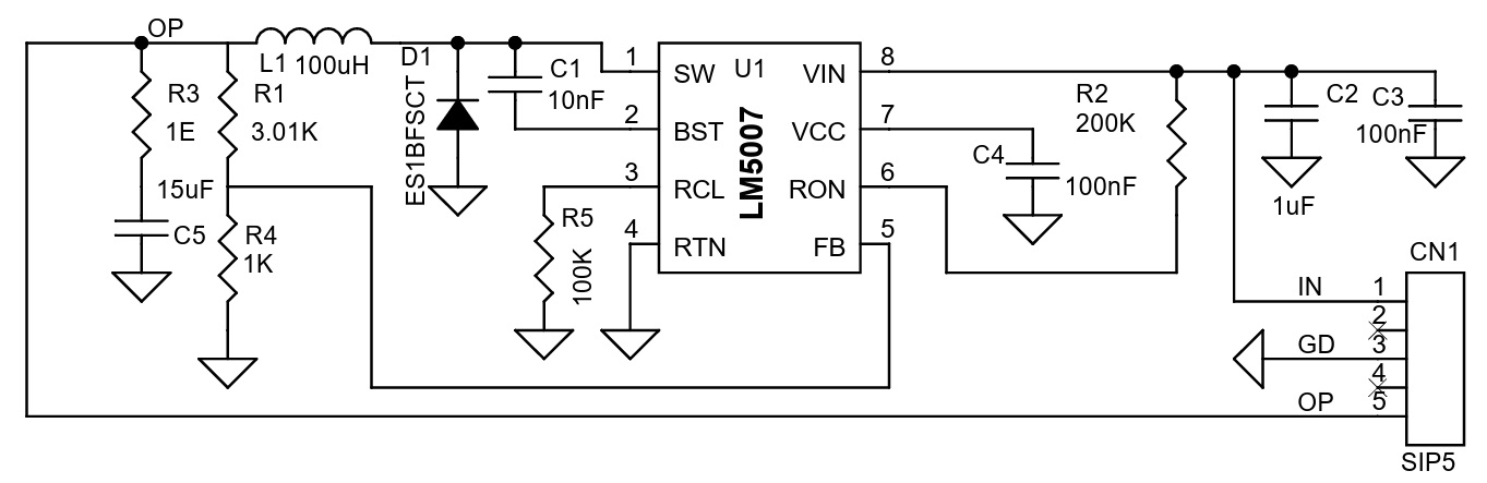
Schematic
Parts List
| NO. | QNTY. | REF. | DESC. | MANUFACTURER | SUPPLIER | SUPPLIER PART NO |
|---|---|---|---|---|---|---|
| 1 | 1 | CN1 | 4 PIN MALE HEADER PITCH 2.54MM | WURTH | DIGIKEY | 732-5317-ND |
| 2 | 3 | CN2,J1,J2 | 2 PIN MALE HEADER PITCH 2.54MM | WURTH | DIGIKEY | 732-5315-ND |
| 3 | 1 | CN3 | 3 PIN MALE HEADER PITCH 2.54MM | WURTH | DIGIKEY | 732-5316-ND |
| 4 | 1 | CN4 | 6 PIN MALE HEADER PITCH 2.54MM | WURTH | DIGIKEY | 732-5319-ND |
| 5 | 4 | U2,Q2,CN5,R6 | DO NOT INSTALL | |||
| 6 | 1 | C1 | 100nF/50V CERAMIC SMD SIZE 0805 | YAGEO/MURATA | DIGIKEY | |
| 7 | 1 | C2 | 10uF/25V CERAMIC SMD SIZE 1210 OR 1206 | YAGEO/MURATA | DIGIKEY | |
| 8 | 1 | D1 | LED SMD SIZE 0805 | OSRAM | DIGIKEY | 475-1278-1-ND |
| 9 | 1 | PR1 | 2K TRIMMER POTENTIOMETER | BOURNS | DIGIKEY | 3296Y-202LF-ND |
| 10 | 1 | PR2 | 500E TRIMMER POTENTIOMETER | BOURNS | DIGIKEY | 3296W-501LF-ND |
| 11 | 1 | Q1 | BC635 TO92 | MULTICORP | NEWARK | 08N8059 |
| 12 | 1 | R1 | 1K 1% SMD SIZE 0805 | YAGEO/MURATA | DIGIKEY | |
| 13 | 1 | R2 | 10K 1% SMD SIZE 0805 | YAGEO/MURATA | DIGIKEY | |
| 14 | 1 | R3 | 0E SMD SIZE 0805 | YAGEO/MURATA | DIGIKEY | |
| 15 | 1 | R4 | 620E 1% SMD SIZE 0805 | YAGEO/MURATA | DIGIKEY | |
| 16 | 1 | R5 | 51E 1% SMD SIZE 0805 | YAGEO/MURATA | DIGIKEY | |
| 17 | 1 | R7 | 1.2K 1% SMD SIZE 0805 | YAGEO/MURATA | DIGIKEY | |
| 18 | 1 | R8 | 1.1M 1% SMD SIZE 0805 | YAGEO/MURATA | DIGIKEY | |
| 19 | 1 | R9 | 120E 1% SMD SIZE 0805 | YAGEO/MURATA | DIGIKEY | |
| 20 | 1 | U1 | LM358 SOIC8 | TI | DIGIKEY | LM358AMX/NOPBCT-ND |
| 21 | 3 | JUMPER | SHUNT FOR JUMPER | SULINS CONNECT | DIGIKEY | S9001-ND |
| 22 | 1 | Sensor Part # | FS2T.0.1E.025 | DIGIKEY | 2952-FS2T.0.1E.025-ND |
Connections
Application Schematic
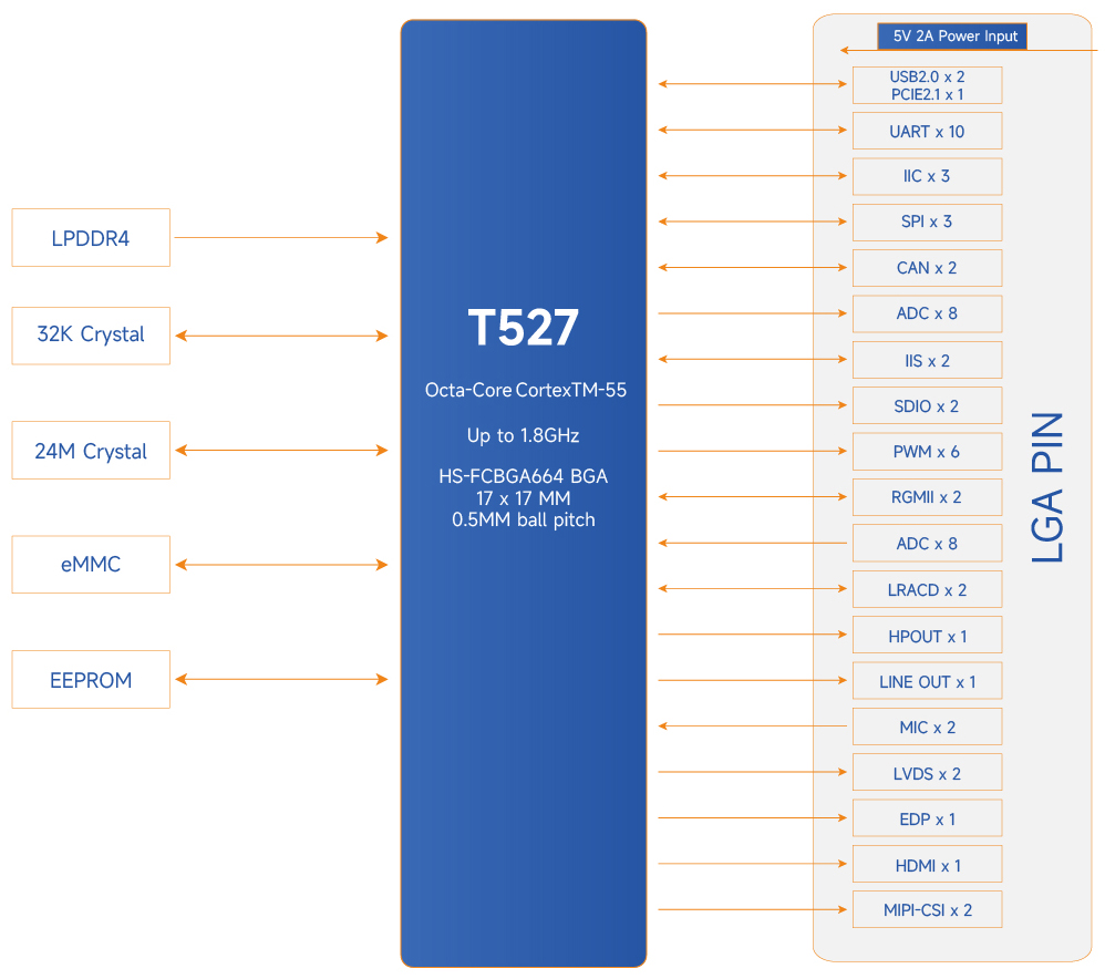
Sensor Details
High Flow Diagram
Gerber View
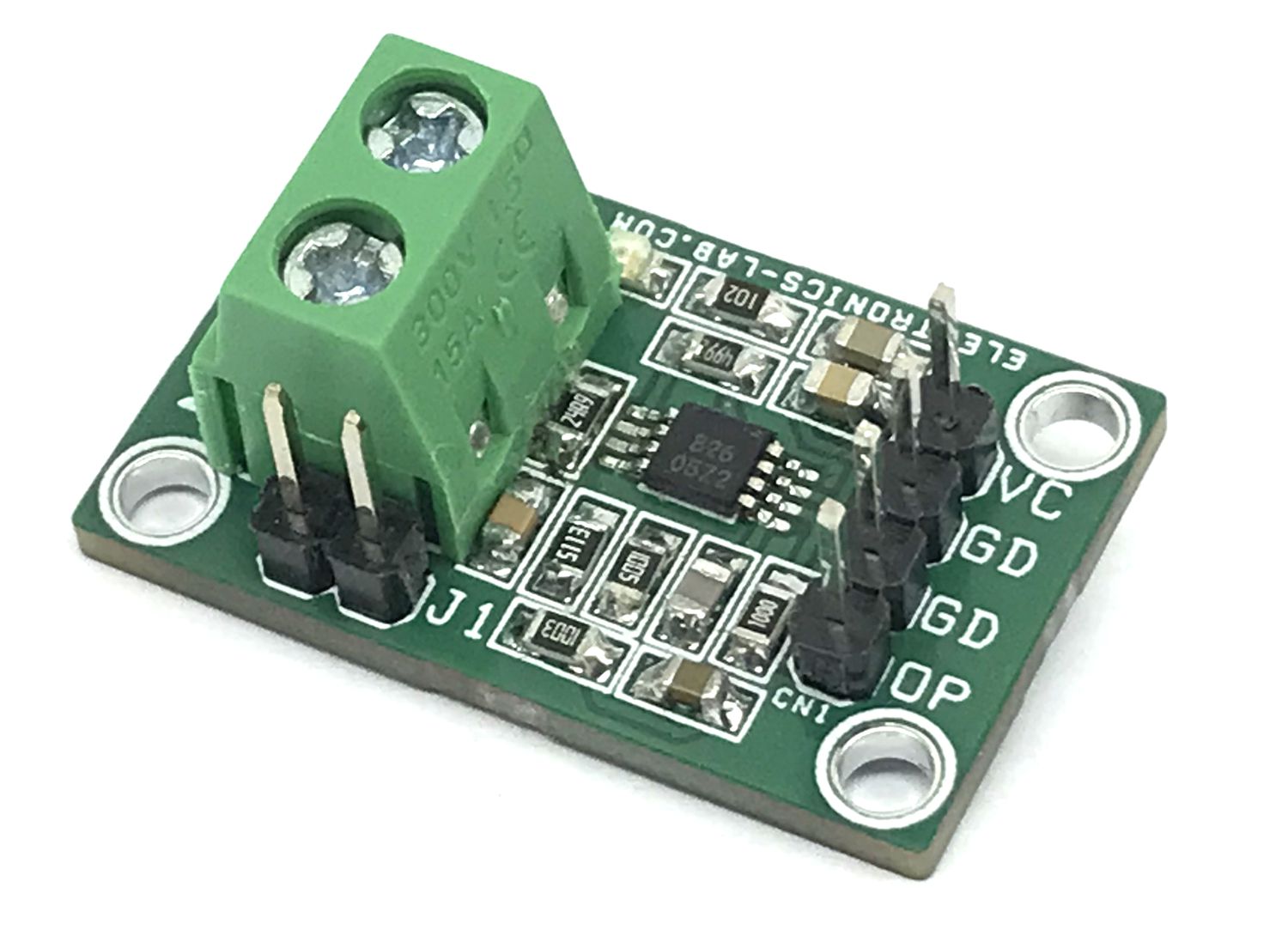
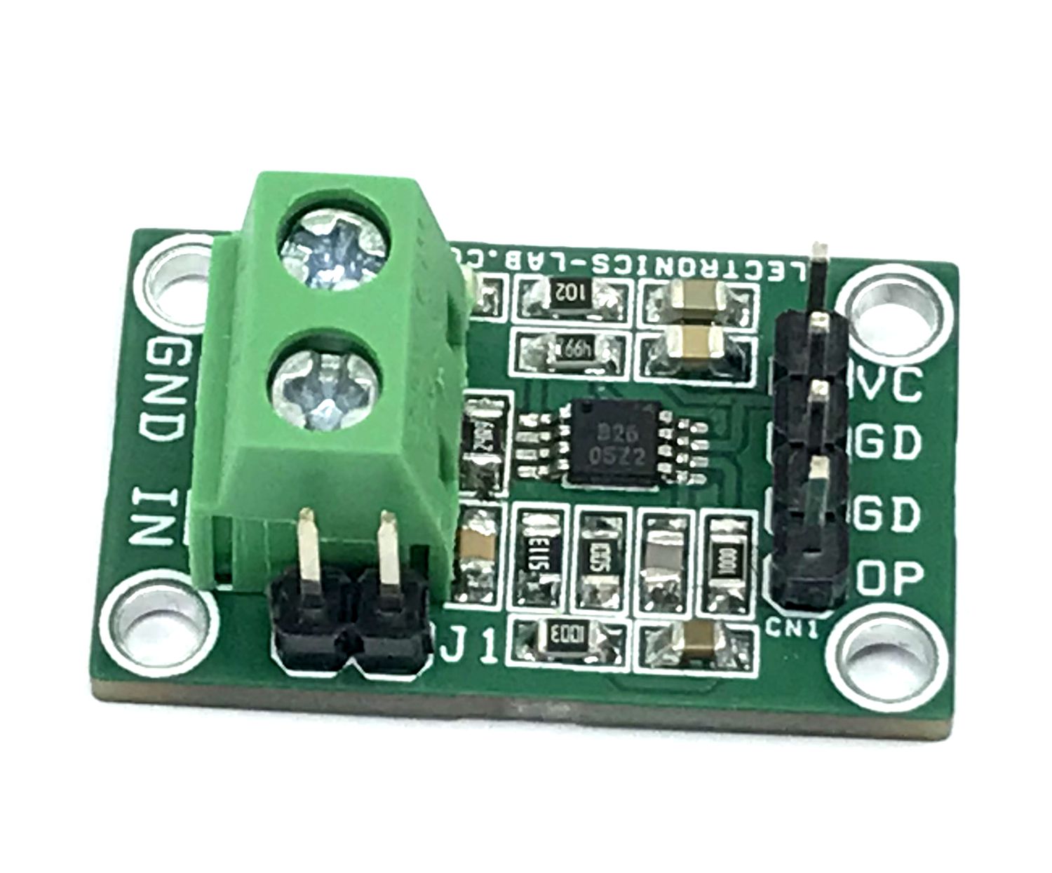
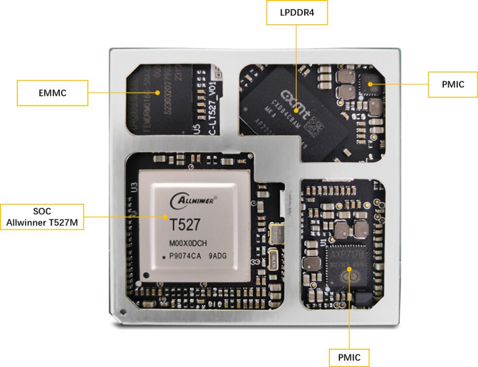
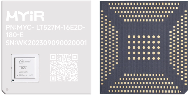
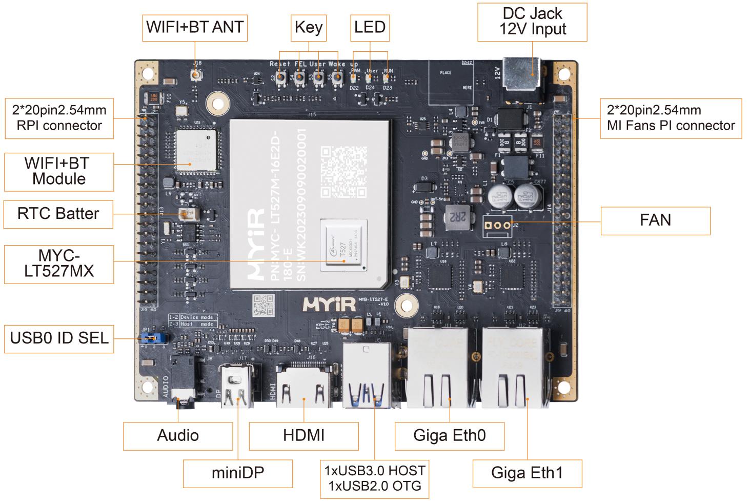
Photos
Video