Texas Instruments Introduces TPS63900 DC/DC Buck-Boost Converter

Texas instruments introduced the TPS63900 DC/DC buck-boost converter; the company is calling it the industry’s first. It combines programmable input current limit and integrated dynamic voltage scaling to extend battery life.

The TPS63900 has a quiescent current of 75 nA with 92% efficiency at 10 µA.

Per a company release, TPS63900 integrates dynamic voltage scaling to deliver power while keeping the system at the minimum voltage required to operate efficiently, maximizing battery life and reducing required maintenance for industrial applications.

The features allows for optimization of power architectures for ultra-low power sensors and wireless connectivity integrated circuits.

The TPS63900 efficiently charges supercapacitors to buffer peak loads, protect battery capacity, and extend system lifetime and performance. By doing so, it helps buffer the energy that is required to operate components that are required for high peak currents.

Further, it increases stability of applications that are connected by reducing up to 50% of the output-voltage ripple caused by load transients. The transient response maintains low IQ, all while keeping internal regulation loop active.

For more information, visit https://www.ti.com/product/TPS63900?HQS=app-bmc-bcs-tps63900-pr-pf-null-wwe

SEGGER J-Link adds support for Raspberry Pi as host

SEGGER has just introduced a version of its J-Link software specifically for Linux Arm. Aimed at industrial automation and other applications utilizing Raspberry Pi and other single board computing platforms, this new package contains all command-line versions of the software. It supports the same target devices and the full feature set encompassed in the already-established Windows, macOS and Linux x86 versions. These features include high-speed download into Flash memory and an unlimited number of breakpoints (even in Flash memory), as well as a J-Link GDB server which makes it compatible with all popular development environments.

The software is available for both 32-bit and 64-bit Arm Linux, taking full advantage of the 64-bit CPU and all memory available in the system. It works on Raspberry Pi, as well as the various compatibles that are now on the market. The J-Link SDK also fully supports the writing of custom programs for J-Link on Arm Linux.

“Although it seems very unusual, even unlikely, it is now possible to use a small Raspberry Pi 4 single board computer with the Eclipse for Embedded C/C++ Developers package and the additional xPack binary tools, plus SEGGER’s J-Link debug probe and J-Link software, to create projects, build them and run debug sessions. Amazing!” says Liviu Ionescu, Developer of the Open-Source Eclipse Embedded CDT project.

“Raspberry Pi is gaining more and more popularity as a small, inexpensive yet powerful multi-purpose computing solution. While the typical use is automated test systems, with the Raspberry Pi acting as a J-Link bridge or server in the LAN/WLAN, there are many other applications. With Eclipse Embedded CDT coming, it is possible to use Raspberry Pi and J-Link as hardware to develop, download and debug firmware for embedded devices.” says Rolf Segger, founder of SEGGER.

About Raspberry Pi

Raspberry Pi was initially designed as an inexpensive way to introduce people to computers and programming, in schools and developing countries. SEGGER’s support for the Pi is in keeping with its philosophy of supporting students and hobbyists. Most of the SEGGER software tools are available at no cost for non-commercial usage under SEGGER’s Friendly License. SEGGER also offers educational versions of the popular J-Link Debug Probe. The J-Link EDU and J-Link EDU Mini are available for educational purposes at minimal cost.

For additional information please visit: www.segger.com

NCR18650BD-Improved, the ultimate generation of safe, smart and stable Li-ion cell

Panasonic’s new NCR18650BD-Improved is the latest evolution of its Li-ion cell – and can be considered as the result of the last years’ efforts to further evolutionize reliability, longevity and performance alongside the requirements of contemporary applications.

“Frankly spoken”, Norbert Depresles, Section Head of Business Development EMEA from Panasonic Industry Europe says,

“the NCR18650BD-Improved fits almost everywhere and demonstrates a proven performance stability over a wide range of discharge rate, temperature and cycle life.”

Nowadays, reliability doesn’t only comprise immaculate safety as a prerequisite, i.e. avoiding issues in terms of damage or even human risks. Reliability is also an economic factor – which is sustainably met by the NCR18650BD-Improved as endurance runner “without airs and graces”,

in particular, because there is no State of Health check (SOH) – an almost traditional restraint for Li-Ion cells – needed under certain charging conditions. By being charged at less stressful 4.15V from the start, this cell does not need the SOH check nor a reduction in the charging voltage. But even with 4.15V charging, the capacity of each cycle is higher and more stable in comparison to PF cells. It can be charged and discharged with high reliability and long life.

“On the meta-level, the NCR18650BD-Improved’s core feature is being unpretentious in every regard,” Mr. Depresles summarizes. “Having it reliably working in almost all environments and thus achieving cost reduction is what everyone needs. I’d even say, with the NCR18650BD-Improved, we have taken a crucial step towards the battery that ‘can be forgotten’ in the positive sense.”

more information: na.industrial.panasonic.com

Aetina Launch New NVIDIA Jetson-based Platform AN810-XNX

Support High Speed Networking Capability Function & Certified Azure IoT

Aetina Corporation, the provider of high-performance GPGPU and edge AI computing solutions, announced the new AN810-XNX edge AI computer leveraging powerful capabilities of the NVIDIA® Jetson Xavier™ NX. This edge AI computer provided various alternatives of I/O slot, nicely expand its range of edge AI systems built on the Jetson platform for robotics, drone, UAV, industrial inspection, medical imaging, and deep learning.

The AN810-XNX combines the NVIDIA Jetson Xavier NX and Aetina brand new AN810 carrier board in a Nano-ITX form factor of 120x120x47.3 mm (with fan). It supports full M.2 slot with M-key, E-key, and B-key and the interface with PCIe/SATA/USB 3.2 Gen2/USB 2.0. AN810-XNX features prospective communication capabilities. Since 5G technology has become a sensation in IoT applications, AN810-XNX integrated with the 4G/5G module beforehand for high-speed wireless connection and data transferring. Meanwhile, AN810-XNX equipped an onboard SIM slot, building seamless global connectivity for edge devices. For better management of numerous edge devices, AN810-XNX supports the Innodisk InnoAGE™ out-of-band management SSD solution through M.2. With this solution, it reduces the massive cost of manually repairing the edge device and primarily minimizes the equipment’s downtime, making the remote-control of the edge device more convenient.

With the widespread use of vision AI application, AN810-XNX supports the single 120-pin connector for MIPI CSI-2 interface. It can handle intensive AI workloads ultra-high-resolution cameras to more accurate image analysis. For backup support, Aetina offers BSP and DTB configuration updates for both standard and customized platforms in their service policy.

Aetina focuses on delivering edge AI computing solutions based on the Jetson platform for embedded applications. NVIDIA Jetson benefits the users by supporting cloud-native technologies across AI solutions and various SDK. Moreover, Aetina AN810-XNX got Microsoft Azure Certified for Internet of Things (IoT), ensuring the IoT solutions could fasten development and work with Microsoft Azure IoT services.

“AIoT environment is diverse and complex. Throughout the edge AI systems, GPU-based platform has the most flexibility and Azure cloud services enhance the overall performance. Benefits the customer with shorter development period.” said Joe Lo, general manager of Aetina.

AN810-XNX, high compatibility platform with well-backup service from edge to cloud, could deploy high-quality, software-defined features on embedded and edge devices targeting robotics, drone, UAV, industrial IoT, healthcare, deep learning, etc.

The AN810-XNX is available now. For more information, please directly contact at sales@aetina.com or visit the website at www.aetina.com

DDR4 NVDIMMs with high speed bus rates

SMART Modular Technologies has launched 16GB and 32GB NVDIMMs that operate on the DDR4-3200 high-speed bus rates. by Ally Winning @ eenewsembedded.com

The new devices combine Micron’s advanced DDR4 DRAM technology and SMART’s high-speed PCB designs. The combination of the two technologies significantly improves signal integrity, providing broader design margins even at the highest DDR4 bus speeds. NVDIMMs have seen broad adoption in applications that need “normal” memory operation at DRAM bus clock rates. SMART’s new NVDIMMs are also developed with Micron’s advanced 3D NAND technology to offer highly reliable memory persistence if the system crashes or there is a power outage, with minimal back-up and restore times.

“We are pleased that SMART is employing Micron’s DRAM and 3D NAND technologies in its newest leading-edge NVDIMM products to offer maximum reliability and performance,” stated Malcolm Humphrey, vice president of marketing of the Compute & Networking Business Unit at Micron. “Enterprises that need resilient memory and storage to ensure constant availability of mission-critical information will benefit from SMART’s NVDIMMs.”

The NVDIMMs operate much the same as DDR4 RDIMMs. They offer unlimited write endurance with integrated persistence capability. These traits create allow for efficient write acceleration and high-speed recovery capability. SMART NVDIMMs provide the full feature set currently defined by JEDEC standards. Additionally, AES-XTS 256 provides enhanced data protection. SMART also provides a wide variety of intelligent back-up power modules (BPM) in different form factors to provide temporary power during back-up operations.

SMART also offers full firmware and technical support to its customers for NVDIMM and BPM products. The company has a 10-year track record of designing, manufacturing and supporting NVDIMMs and BPMs. It has been a key contributor, along with other industry partners, in establishing the evolving NVDIMM ecosystem.

more information: www.smartm.com

Broadcom ACNT-H511C high CTI optocoupler

The ACNT-H511C is a single-channel open collector optocoupler device in 15-mm stretched SO8 package

The ACNT-H511C is a single-channel open collector optocoupler device in 15-mm stretched SO8 package. The device is equipped with an insulating layer between the light-emitting diode and an integrated photon detector to provide electrical insulation between the input and output. Having separate connections for the photodiode bias and output transistor collector reduces the base-collector capacitance and enhances the data speed up to a hundred times compared to a conventional photo-transistor coupler.

Key features

  • More than 600 V CTI,  Material Group I
  • 15 mm Stretched SO8 Package
  • TTL Compatible
  • Open-Collector Output

Additional features

  • High CTI, open collector output optocoupler in 15 mm stretched SO-8 package
  • Guaranteed AC and DC performance over wide temperature: -40 to +105 °C
  • Wide operating Vcc range: 4.5 to 24 V
  • Internal clearance (DTI): 0.5 mm
  • 40 kV/μs typical common-mode rejection (CMR) at VCM = 1500 V
  • Safety and regulatory approvals:
    • UL 1577 Recognized: 7500 VRMS for 1 minute
    • CSA approved
    • IEC/EN 60747-5-5 approved for reinforced insulation:
      • VIORM = 2262 VPEAK
      • VIOTM = 12000 VPEAK

Applications

  • High-voltage power systems, for example, 690V AC drives
  • Renewable energy inverters
  • Feedback elements in switching power supplies
  • Digital isolation for A/D, D/A conversion digital field
  • Communications interface
  • MCU interface

more information: www.broadcom.com

Type K Thermocouple Sensor Amplifier Arduino Shield

This is a Type K Thermocouple Sensor Amplifier Arduino Shield that enables an Arduino board to acquire temperatures from a thermocouple of type K. The shield works with a single supply and takes 5V DC from the Arduino board, the output of the circuit is 0 to 4V DC for 0-degree centigrade to 400C. The output of the amplifier is connected to the A0 analog pin of Arduino. A typical application of thermocouples is in boilers, soldering stations, and heaters. Also, 3D printers rely on thermocouples to measure the extruder temperature.

Type K Thermocouple Sensor Amplifier Arduino Shield – [Link]

High density robust SSD offers densities up to 1TB in a 16×20 mm BGA

2100AI/AT SSD Family – High density robust SSD offers densities up to 1TB in a 16×20 mm BGA

Micron has officially launched the Micron 2100AI/AT– an industrial- and automotive-grade PCIe NVMe Industrial SSD family based on 64-layer triple-level cell (TLC) 3D NAND technology. Available in 64GB-1TB BGA and 256GB-1TB M.2 form factors, the new 2100AI/AT series is Micron’s first offering with a PCIe interface supporting the NVMe protocol that is designed to address the needs of the industrial segment: longevity, reliability, quality, ruggedness, and application-specific features such as namespace, autonomous power transitions, and boot emulation.

These SSDs are ideally suited for the Aerospace and Defence market combining an extended temperature range and robust data protection features, along with Micron’s long-term product commitment and customer collaboration, creates a design that stands apart from the competition.

Designs that require high endurance can take advantage of application-specific features provided by these PCIe NVMe SSDs, such as namespace. With the namespace feature, a portion of the SSD (or the entire SSD) can be converted to SLC mode.

In addition to having a removable M.2 form factor, the BGA form factor offers a highly ruggedized solution for industrial applications—providing up to 1TB of storage space. Systems requiring greater than 1TB can utilize multiples of these devices to take advantage of the 16mm x 20mm package size.

Benefits

  • Extended Temperature Ranges: Withstand extreme environments via an industrial temperature range (2100AI: –40°C to 95°C), and automotive temperature range (2100AT: –40°C to 105°C), and adaptive thermal throttling.
  • Robust Data Security: Protect data with industry leading and on-the- fly hardware-based encryption, secure firmware download, and cryptographic erase.
  • Data Path Protection: Help protect user data as it passes through the SSD.
  • Power-Loss Protection: Protect data at rest, helping to ensure data integrity in unexpected power-loss events.
  • Responsive Performance: Deliver significantly faster boot, file and application load times compared to traditional hard drives.
  • Low Power Consumption: Consume considerably less power than typical hard drives.​

more information: www.micron.com

Advantech Releases High-Performance 3.5″ SBC MIO-5373 with 8th Gen. Intel® Core™ Processors

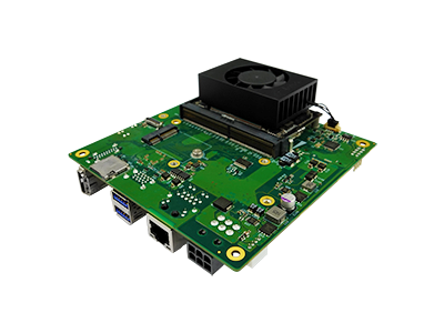
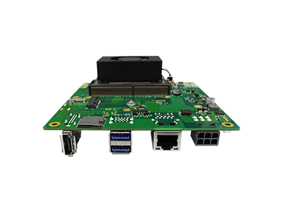
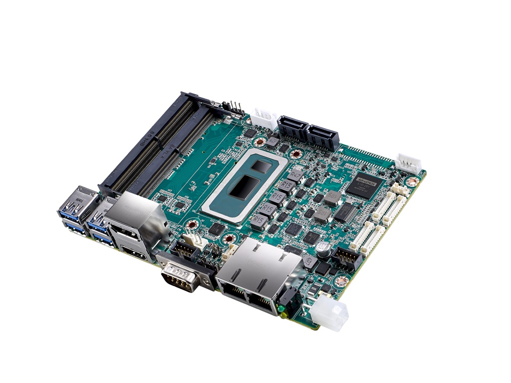
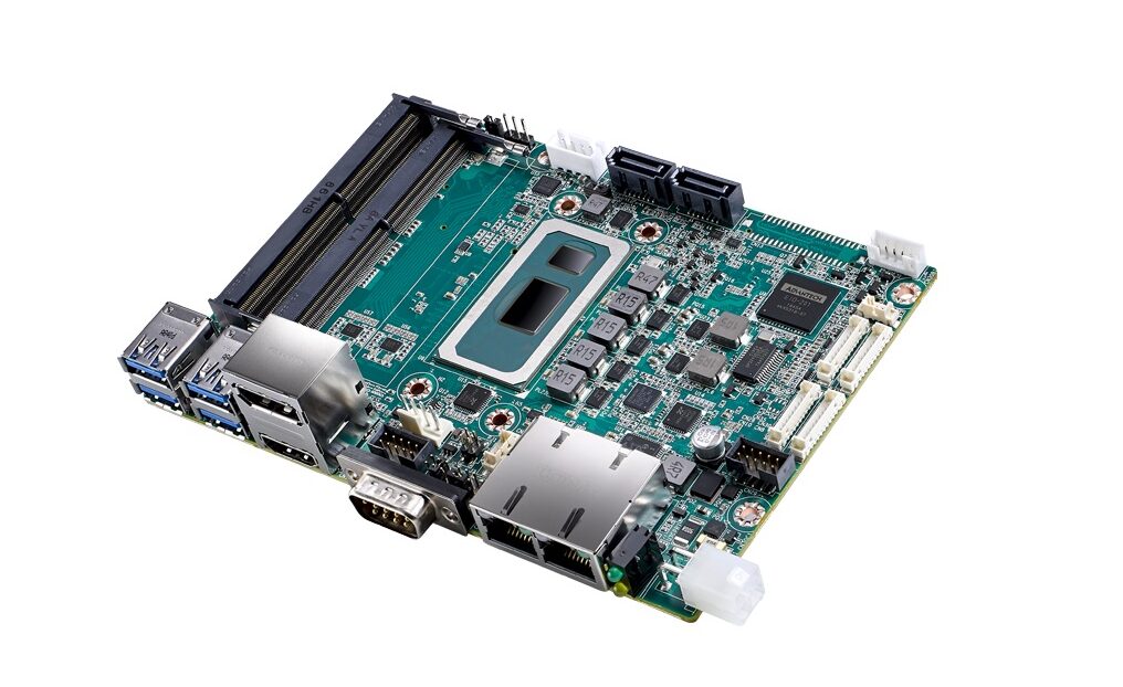
Advantech, a leading global provider of IoT systems and embedded platforms, is pleased to announce the latest 3.5″ SBC MIO-5373 based on the low power 8th Gen. Intel Core SoC. Featuring compact 146 x 102 mm dimensions, the MIO-5373 design not only offers impressive I/O functionality but also provides domain-focused features like CANBus and wide-range power input. It is ideally suited for use in application fields like medical equipment, automation control systems, outdoor kiosks, and areas requiring small dimensions and Intel Core-level computing power.

Quad-Core Performance and High Speed NVMe x4

The new 8th Gen. Intel Core low-power SoC (codename: Whiskey Lake-U) is the first generation to double the computing cores from dual to quad. This new generation provides up to 40% Multi-threaded computing performance over previous generation processors at a TDP of just 15 Watt. Featuring a built-in Gen9LP graphics engine, MIO-5373 supports three simultaneous displays through LVDS/eDP, HDMI, and DisplayPort interfaces up to 4K resolution, as well as H.265/HEVC, H.264/AVC, MPEG2 hardware decode/encode. The MIO-5373 supports Dual channel DDR4 memory up to 32GB(64GB*) and the M.2 M-Key 2280 for NVMe supports high-speed PCIe x4 SSDs, providing extremely high memory and mass storage data rates. Enhancing overall system performance—rather than just that of the core processor—makes the MIO-5373 very well-suited for image processing in medical applications or heavy loading content kiosk displays.

*64GB DDR4 memory supported with selected SO-DIMM modules.

Domain-Focused I/O and Flexible Expansion

MIO-5373’s built-in iManager 3.0 is based on Advantech’s EIO-201 embedded board management controller, which integrates power sequence control for higher reliability and generic functions including GPIO, hardware monitoring, smart fan control and watchdog timer. It also has domain-focused features like high-speed RS-232/422/485 up to 1Mbps, I2C (100kb/400kb/1Mb) and CANBus. iManager provides I/O functionality in company with drivers and software APIs on both the Windows and Linux operating systems to make it easier for software development. MIO-5373 provides adequate expansion for a variety of function cards, including M.2 E-Key for WiFi+BT or AI acceleration card, M.2 B-Key for 3G/LTE modules or SATA SSD’s  (optional with M-key for high-speed NVMe/PCIex4 SSD’s) What’s more, Advantech’s MIOe Extension interface provides 4x PCIe x1/USB/LPC/SMBus slots for vertically-focused or customized expansion. The MIOe-260 I/O module provides additional 2x GbE, 8x UART, 4x USB, 2x isolated CANBus, 1x miniPCIe socket and 1x M.2 B-key socket. Together with MIO-5373 and MIOe-260, it enables factory automation processes for AGV, CNC machines, or medical equipment I/O requirements.

Wide-Ranging Power Inputs and an Extended Operating Temperature Range

MIO-5373 comes with a 12-24VDC wide-range power input that easily connects to factory power rails or outdoor equipment with HVAC systems inside. To deal with extreme outdoor temperature conditions, MIO-5373 variants are available supporting operation from -40°C to 85°C. The advanced thermal solution leverages four symmetrical heatsink screw holes around the CPU to dramatically lower thermal resistance between CPU and heatsink and help heat quickly dissipate into air. MIO-5373 effectively solves temperature and thermal issues that often confront outdoor kiosks, railways, and crucial factory environments.

WISE-PaaS/DeviceOn: Value-Added Software and Cloud-Based Manageability

MIO-5373 provides ready-to-use Windows 10 and Ubuntu images in company with iManager software API and SUSI utility. Advantech’s WISE-PaaS/DeviceOn—IoT device operations and management software—makes it easy to integrate, visualize, operate, and manage industrial IoT devices through public or private clouds. With DeviceOn’s easy-to-use interface, users can monitor device health, enjoy real-time control over power on/off, troubleshoot, and perform updates over-the-air (OTA), on-site and remotely.

Product Features and Specifications:

  • 8th Gen. Intel® Core i7-8665UE/i5-8365UE/i3-8145UE
  • Dual channel DDR4-2400MT/s with up to 32GB and 32GB eMMC onboard
  • Triple simultaneous displays with 48-bit LVDS/eDP+HDMI+DP, up to 4K resolution
  • Dual GbE, 4x USB3.0, 2x RS-232/422/485, CANBus, 12-24VDC input
  • M.2 E-key 2230 for WiFi+BT, M.2 B-key 2280 for SATA SSD’s or 3G/LTE (optional M.2 M-Key 2280 for NVMe PCIe x4 SSD’s)
  • MIOe extension interfaces with 4x PCIe x1 (configurable as 2×2/1×4), DDI, USB, LPC, SMBus
  • Supports iManager software APIs for Windows 10 and Linux
  • Supports WISE-PaaS/DeviceOn

more information: www.advantech.eu

Meet the RFL-Watch: LoRa-Based Text Communicator

While adulations were still being showered on his work on the MORPHESP 240, Dr. Philippe Cadic (@Sulfroid on twitter), recently shared progress on another project called the RFL-Watch, via his twitter handle which is usually loaded with reports on the progress of his projects.

Based on the RAK4260, the RFL-Watch is a wearable LoRa communicator device which at the very least is expected to be able to tell time among other features.

The maker community for a while has been clamoring for an integrated Lora-MCU module similar to what is available with the ESP8266, with MCU and communication integrated into a single module. A number of LoRa-STM32 modules from Murata and STM themselves, have in the past seemed like a possible way out, but they require extra effort in RF design and certification, and Murata has a minimum order requirement (above 100 units), all of which puts the modules in a different category to modules like the ESP. The amount of LoRa-MCU vendor solutions in the market has increased, but it’s safe to say one of the few that has truly spoken to the pain point of makers has been the RAK4620 and @Sulfroid is already putting the module to use with this Watch.

The RAK4620, based on Microchip’s ATSAMR34J18B, combines a 32-bit ARM Cortex -M0+ MCU with a LoRa Transceiver in a compact surface-mount package, with key features including; Full support for 862 to 1020 MHz frequency coverage (all LoRaWAN® bands), High level of accuracy and stability (32MHz TXCO), Max Tx Power: 20dBm, Max Sensitivity (SF12 BW125kHz):  -136dBm, 17mA (typical) RX Current, and a rich selection of interfaces( I2C, SPI, ADC, UART, GPIOs).

While the work on the RFL-Watch is still in progress, the watch, asides the primary time-telling functionality, comes with a display, a 240 x 240 pixel, high-DPI, IPS LCD, through which a LoRa based text communication is expected to be implemented.

The project is still evolving and the final destination is still largely unclear, but you can follow the development process by checking out the twitter handle of the good Dr.(@sulfuroid). 

We will also provide you with more information as things unfold. Stay tuned!

TOP PCB Companies