One growing trend across the embedded systems development world is the development of boards, Microcontrollers, and general development platforms, that aim to be more inclusive, with respect to supporting other programming languages asides the traditional C/C++ that are synonymous with embedded development. From boards like the Espruino which supports Javascripts out of the box, these boards reduce the embedded system barrier of entry in a way that allows developers from other backgrounds like Software to quickly get up and running on hardware projects. With a lot of ground a language still to cover, a new board, developed by the folks at MadMachine, is taking things further with support for Swift; the programming language popular among iOS developers.
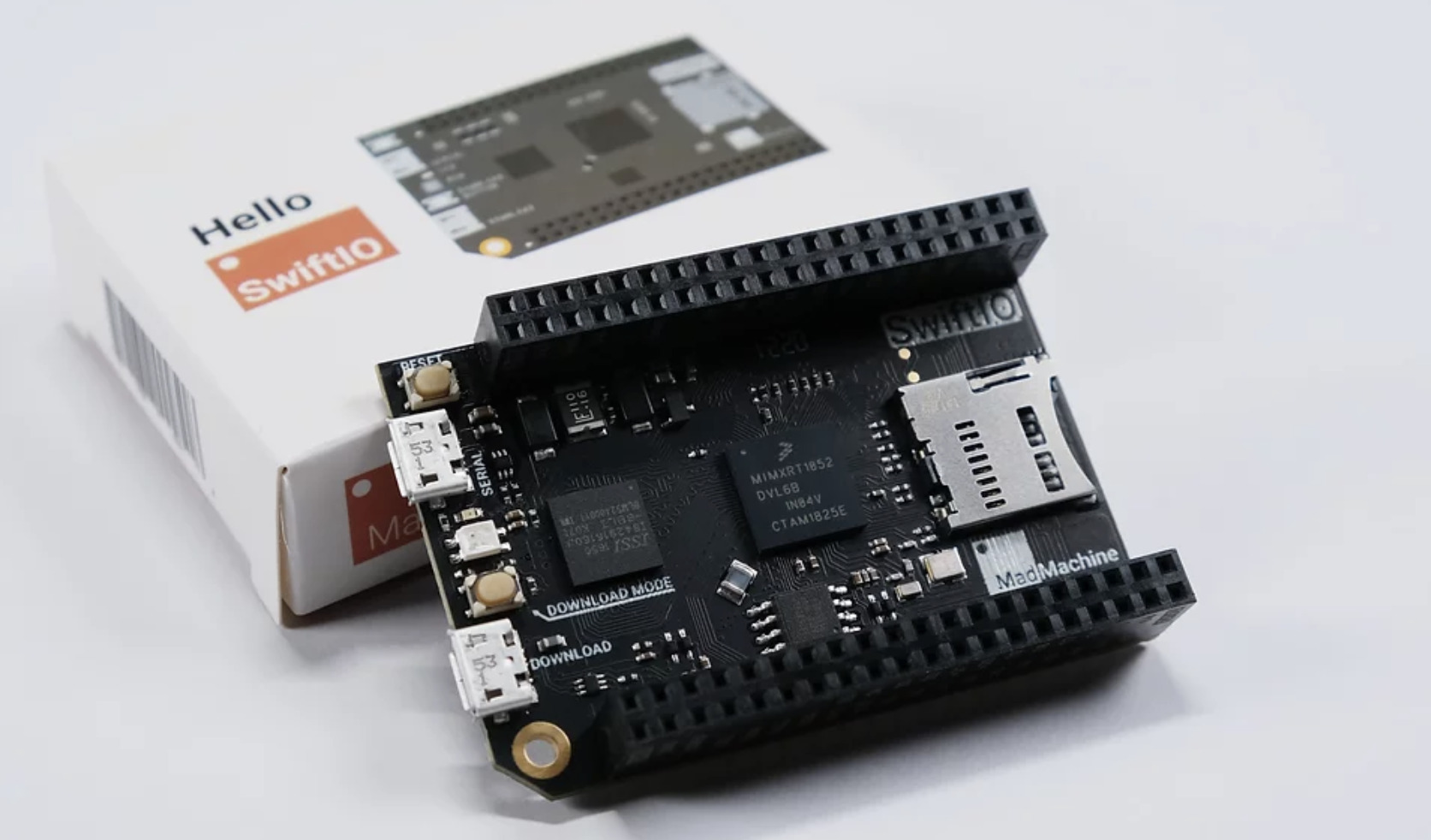
The new board called; the SwiftIO board, is a compact electronics development board that runs Swift on the bare metal, giving you a system that can be used for the development of all kinds of electronics. The design of the board took a cue from the ease and fun associated with the Arduino and it thus supports a range of sensors, lights, and motors that are plug-and-play compatible with Arduino boards.
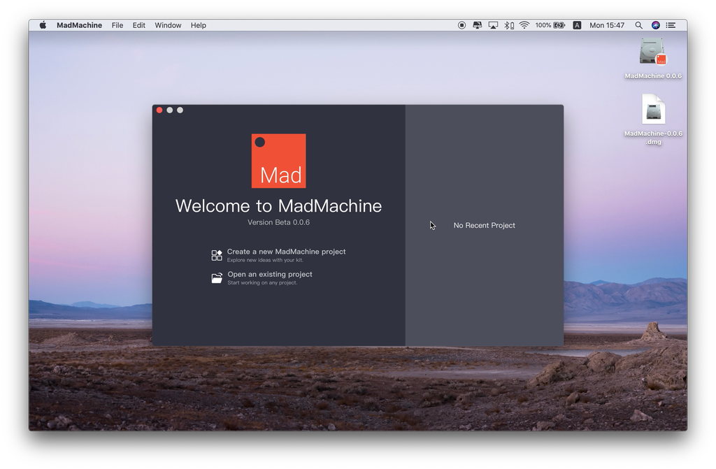
The new development board is accompanied by the MadMachine IDE which offers a full Swift compiler and framework environment that runs on the microcontroller making the development process easy. Despite being popular only among iOS developers, Swift is regarded as a modern general-purpose programming language that incorporates modern approaches to ensure safety, performance and support the implementation of a well-built software design patterns.
The modern and safety features of Swift as a programming language makes it perfect for the future of IoT development and MadMachine is hoping to provide designers with the tools required to leverage those features.
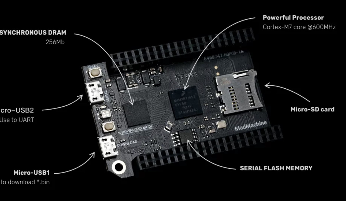
Some features of the SwiftIO board include:
i.MX RT1052 Crossover Processor with Arm® Cortex®-M7 core @600MHz
Micro SD card slot, supporting standard and high capacity SD cards
Micro USB connector for power
On-board USB to UART for serial communication
46 GPIO on left and right edges
On-board GRB LED
12x 12-bit analog to digital (ADC) converters
4 UART, 2 CAN, 2 IIC, and 2 SPI
14 PWM pins
Asides providing a platform for makers to build amazing solutions, MadMachine also hopes the SwiftIO development board will provide a cheap path for makers beginners and enthusiasts that are interested in learning the Swift programming language since the cost of the SwiftIO board is 80% lower than that of the cheapest Apple iPad.
The board is currently available for sale on MadMachine’s store for $68 and users have the option of picking up the SwiftIO maker kit containing different sensors and actuators alongside the SwiftIO board, for $118.
More information on the board, pricing, availability, and features, can be found on MadMachine’s Website.
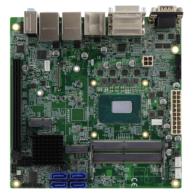
IBASE Technology Inc. (TPEx: 8050), a leading provider of industrial motherboards and rugged computing solutions, has launched the MI996 Mini-ITX motherboard that is powered by the latest 9th Gen Intel Xeon E and Core™ processors. Designed for a wide array of applications such as medical, industrial automation and kiosks, it supports integrated GPU and PCI-E x16 for a discrete graphics card to run simultaneous displays in four video outputs: eDP, HDMI (2.0a), Display Port and DVI-D.
The compact MI996 is suitable for space-constrained applications and packs powerful functionality into a compact Mini-ITX form factor (170mm x 170mm). Enhanced I/O connectivity and expansion comprises six USB 3.1, four USB 2.0, four serial ports, four 4x SATA III, a Mini PCI-E, as well as two M.2 slots for NVMe storage and CNVi WiFi or Bluetooth connections. It features two Gigabit LAN and up to 32GB of DDR4-2666 SO-DIMM memory (ECC and non-ECC) for high-performance computing.
Two model series of MI996 are available with the Intel CM246, QM370, and HM370 chipsets to support a range of Intel processors. Other advanced features include a watchdog timer, Digital I/O, iAMT (11.6) remote management, TPM (2.0) security, iSMART (3.8) green technology, and vPRO (MI996VF series). By consolidating superior performance, versatility and scalability, the MI996 enables system integrators to deliver a highly optimized embedded solution to their customers.
MI996 FEATURES:
Onboard 9th Gen Intel® Xeon® E / Core™ i7/i5/i3 / Celeron® processors
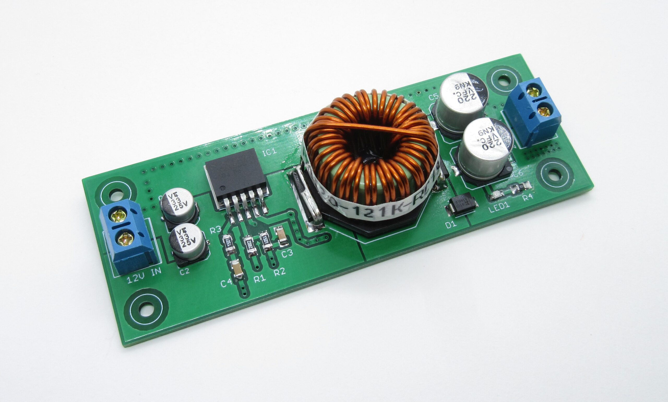
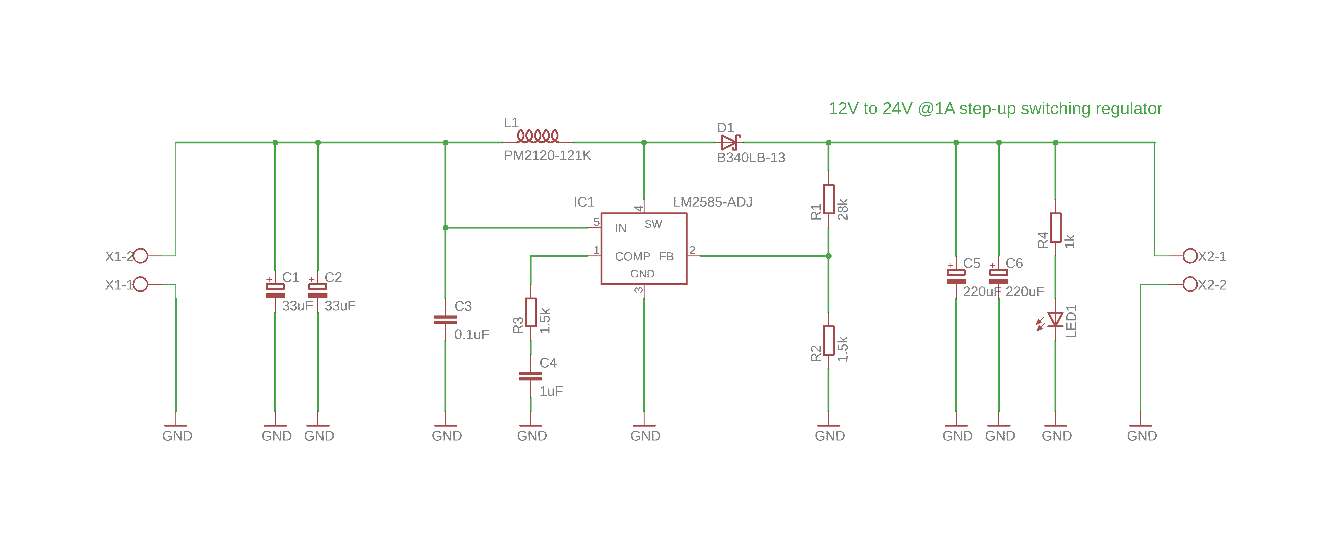
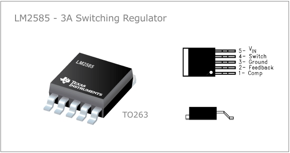
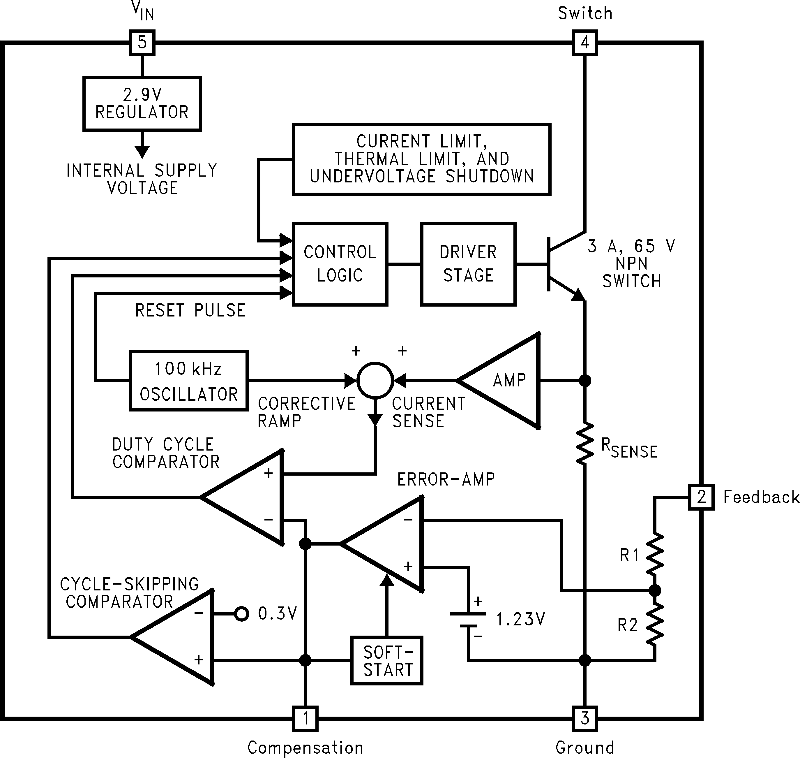
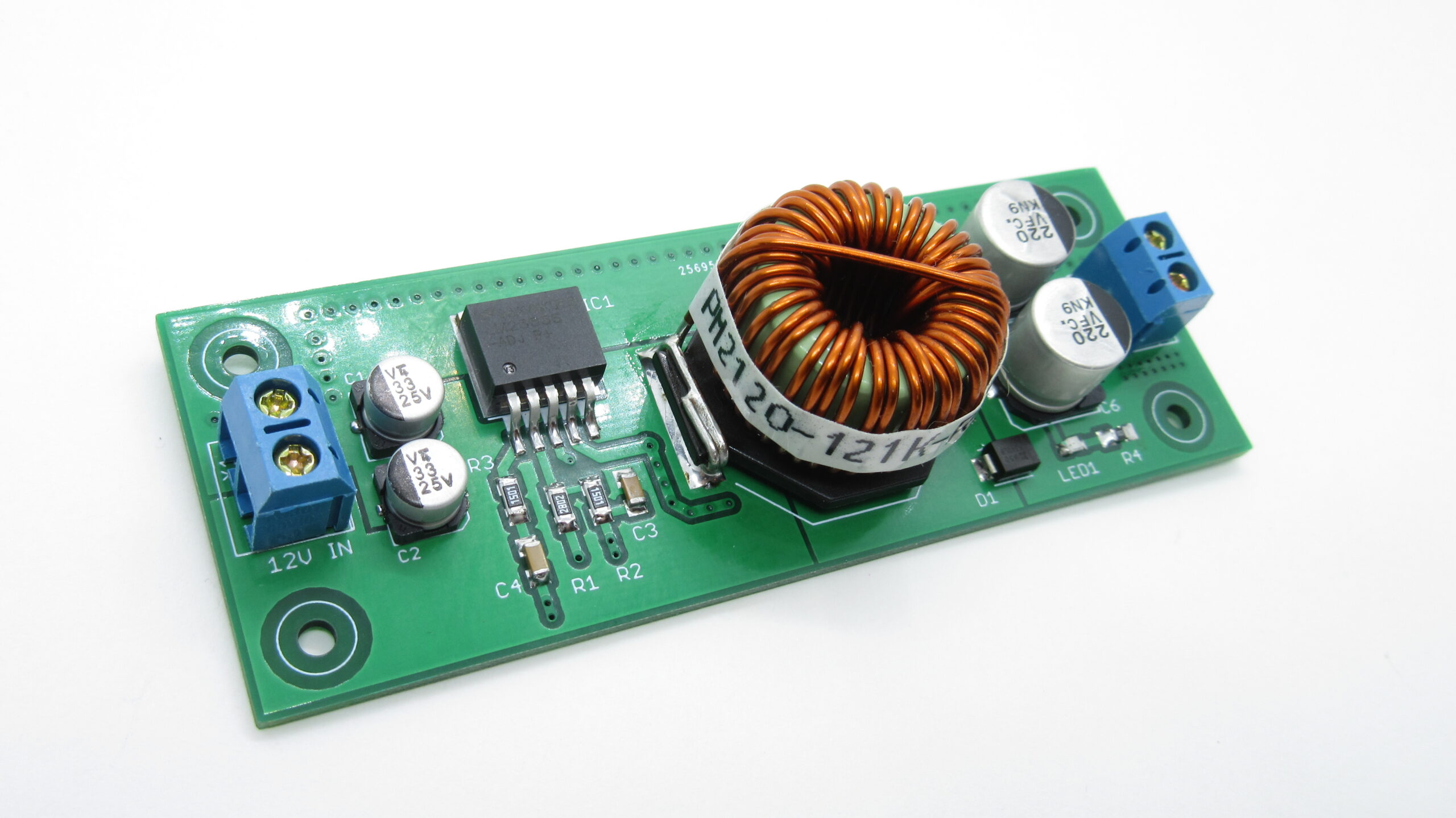
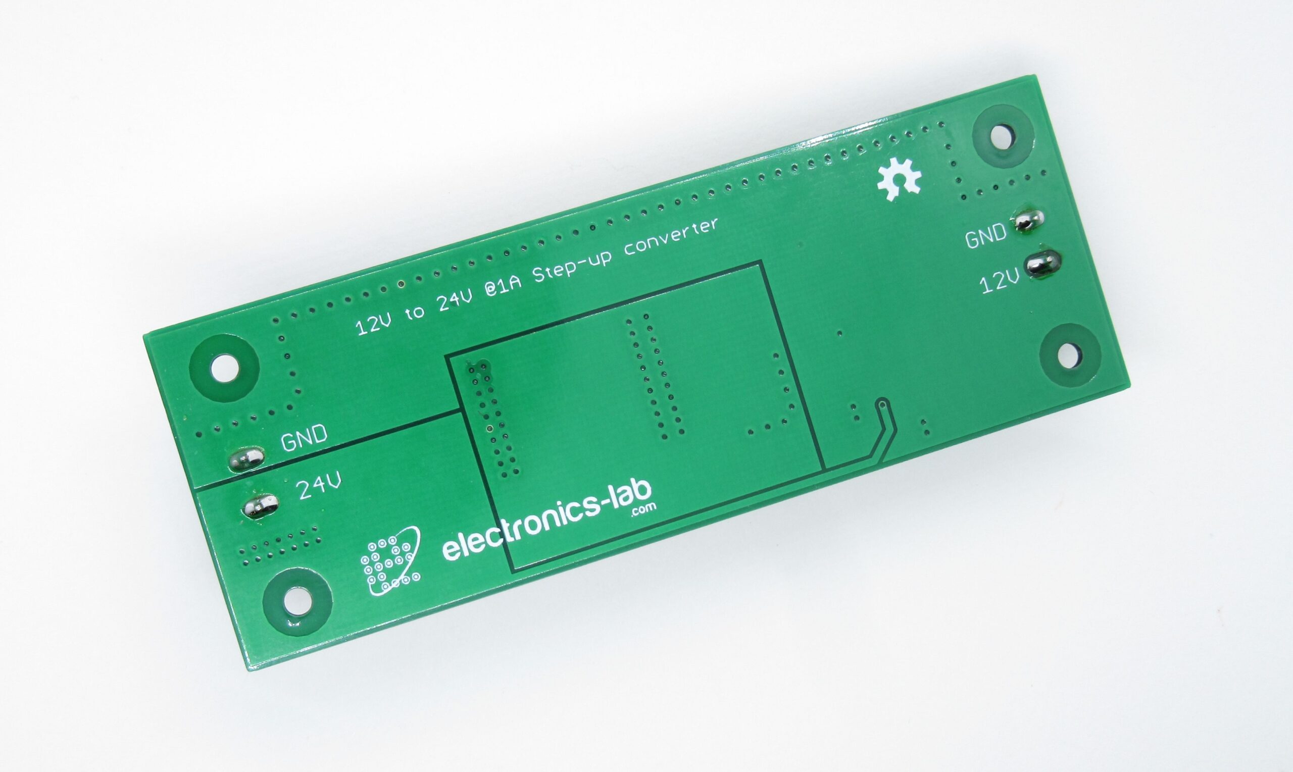
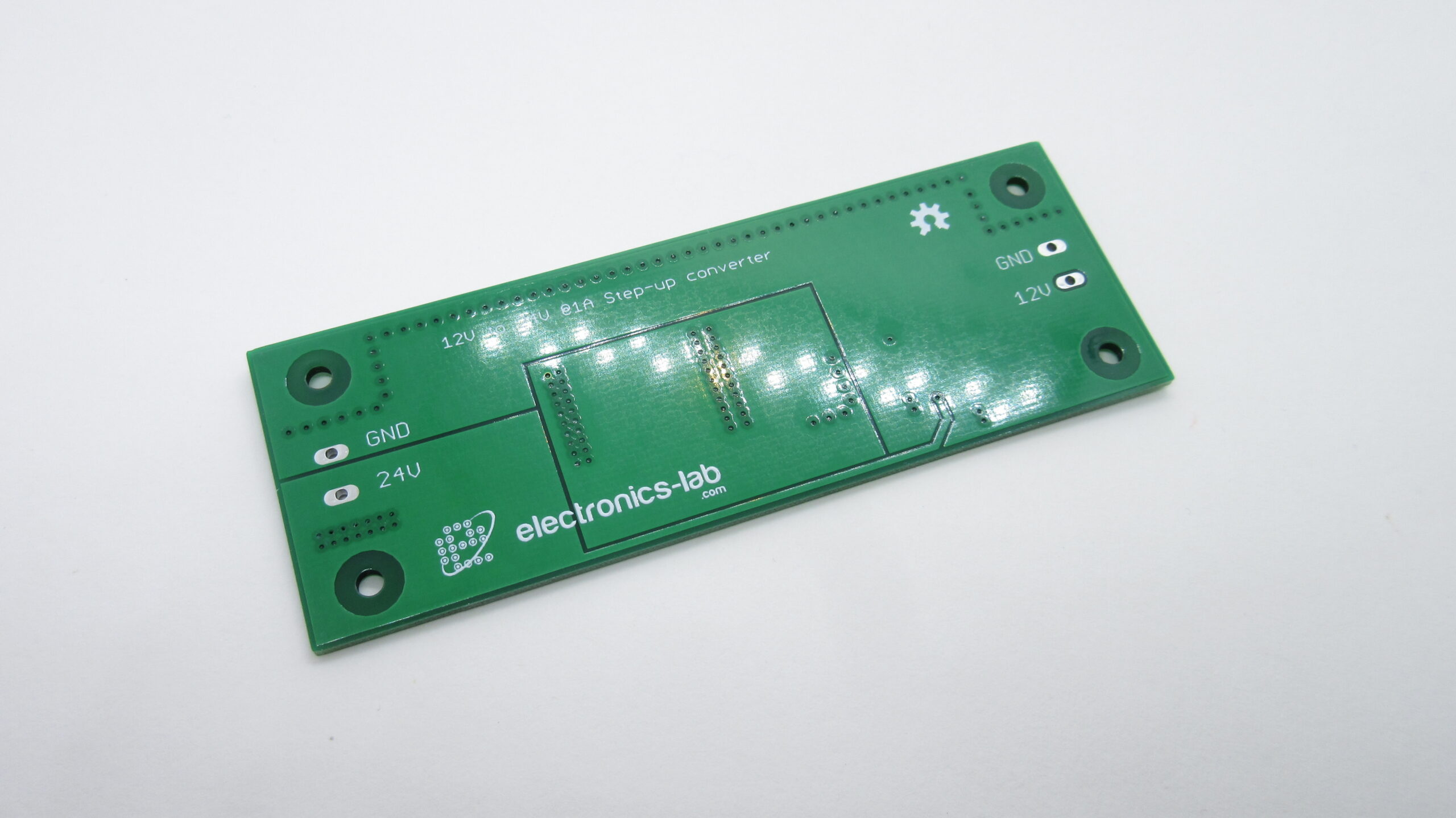
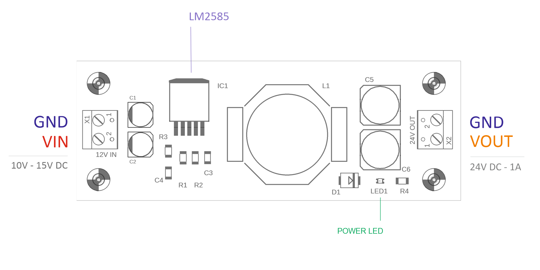
This is a DC-DC step-up converter based on LM2585-ADJ regulator manufactured by Texas Instruments. This IC was chosen for its simplicity of use, requiring minimal external components and for its ability to control the output voltage by defining the feedback resistors (R1,R2). NPN switching/power transistor is integrated inside the regulator and is able to withstand 3A maximum current and 65V maximum voltage. Switching frequency is defined by internal oscillator and it’s fixed at 100KHz.
The power switch is a 3-A NPN device that can standoff 65 V. Protecting the power switch are current and thermal limiting circuits and an under-voltage lockout circuit. This IC contains a 100-kHz fixed-frequency internal oscillator that permits the use of small magnetics. Other features include soft start mode to reduce in-rush current during start-up, current mode control for improved rejection of input voltage, and output load transients and cycle-by-cycle current limiting. An output voltage tolerance of ±4%, within specified input voltages and output load conditions, is specified for the power supply system.
Specifications
Vin: 10-15V DC
Vout: 24V DC
Iout: 1A (can go up to 1.5A with forced cooling)
Switching Frequency: 100KHz
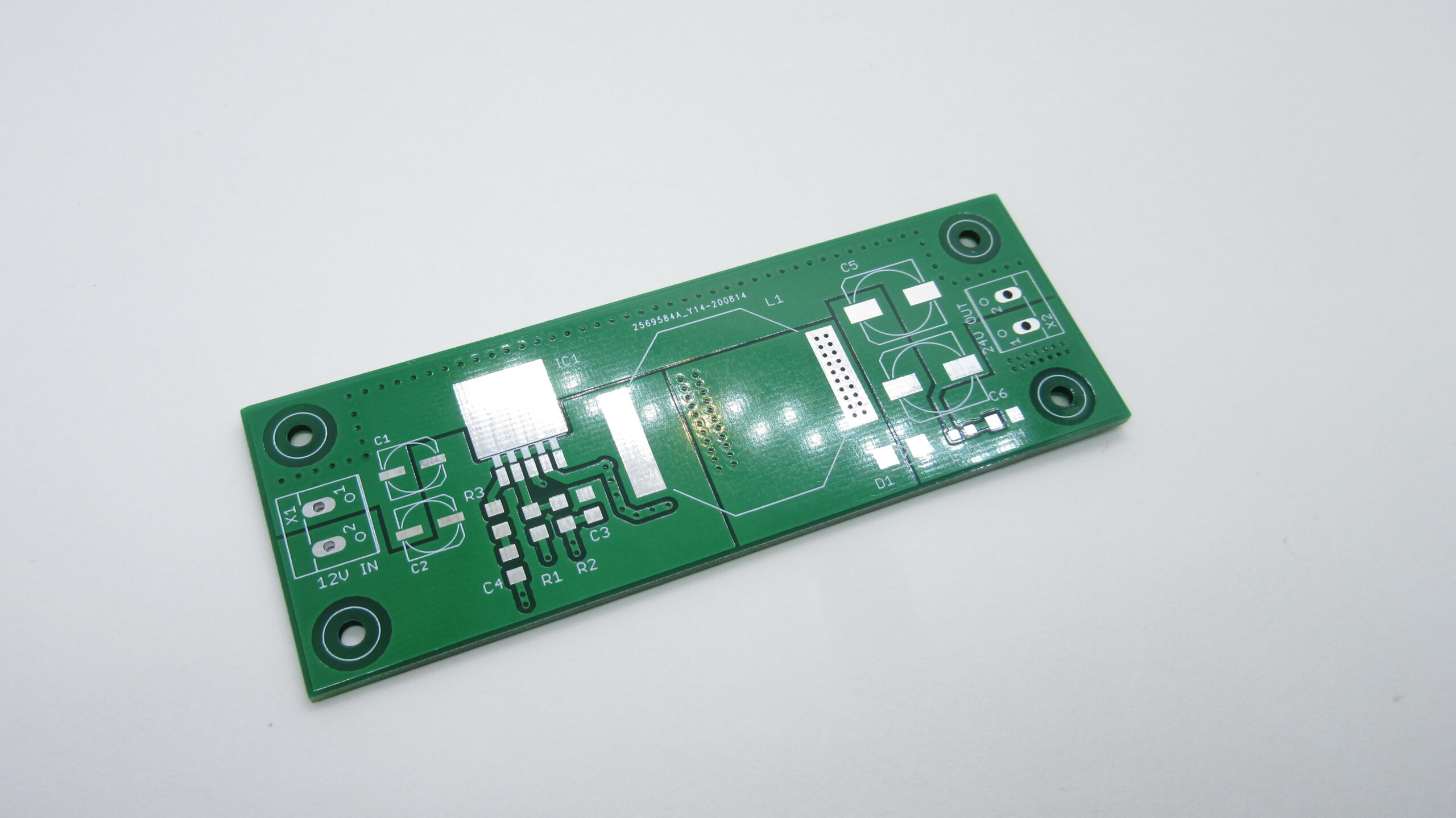
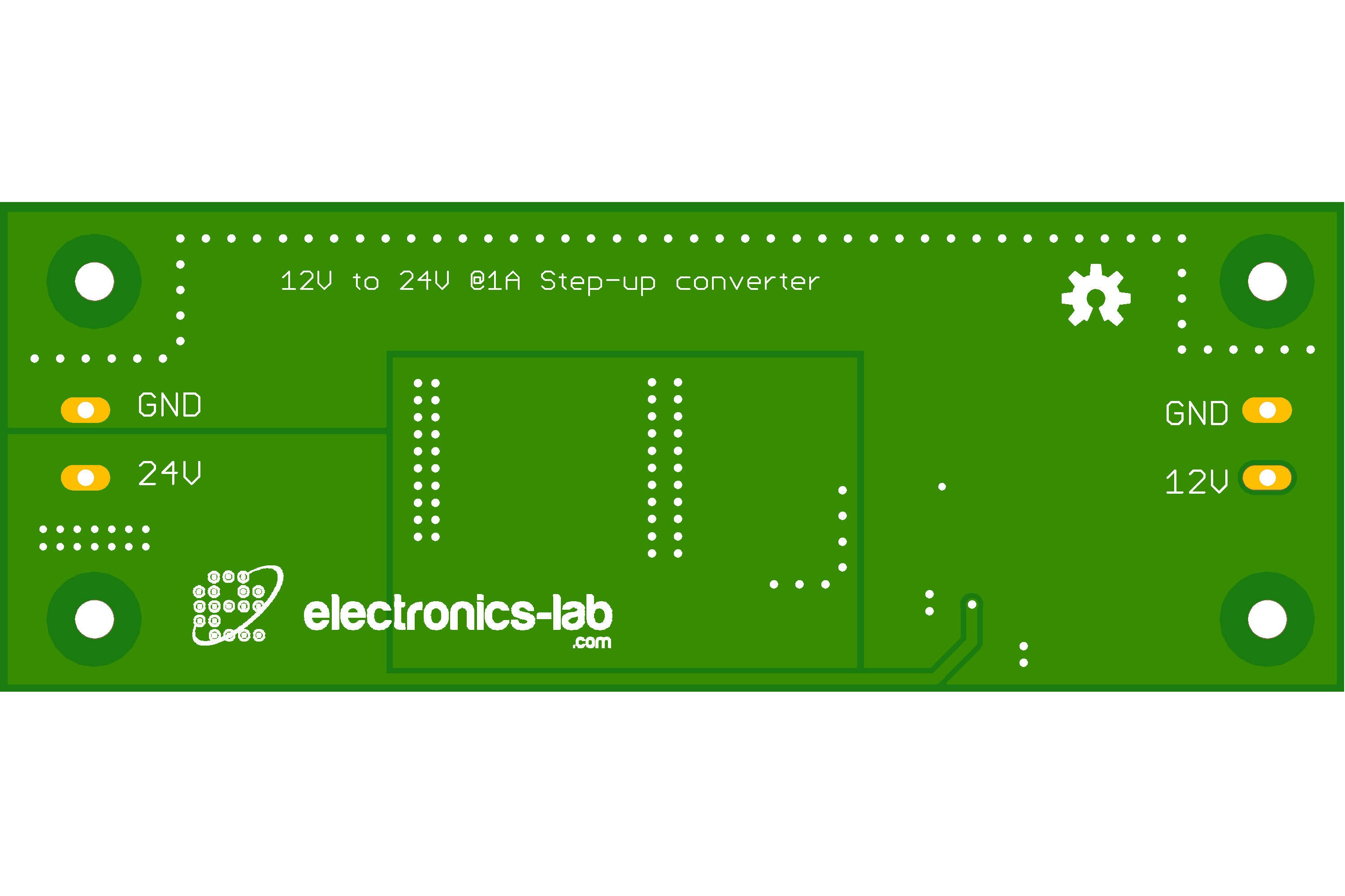
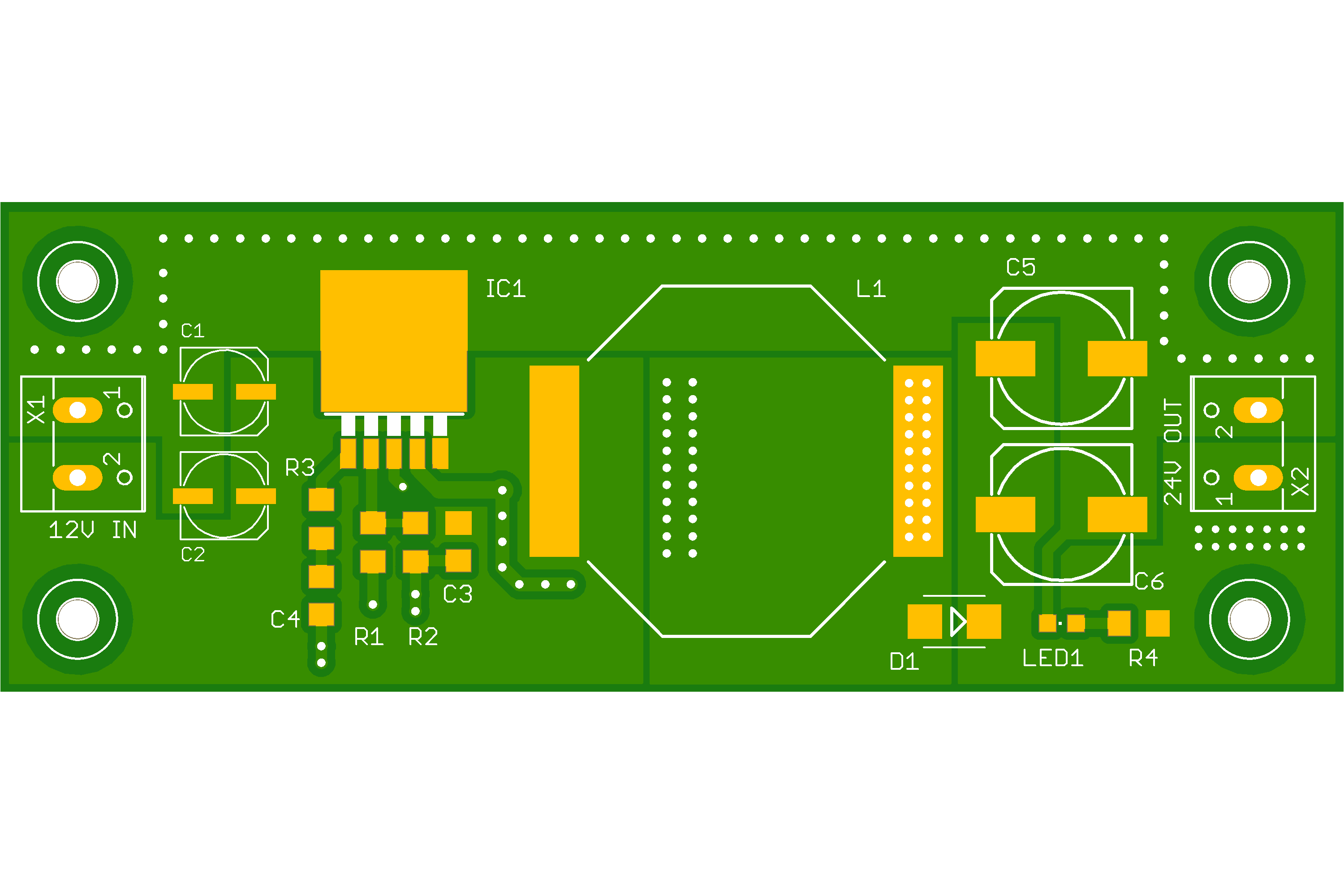
Schematic is a simple boost topology arrangement based on datasheet. Input capacitors and diode should be placed close enough to the regulator to minimize the inductance effects of PCB traces. IC1, L1, D1, C1,C2 and C5,C6 are the main parts used in voltage conversion. Capacitor C3 is a high-frequency bypass capacitor and should be placed as close to IC1 as possible.
All components are selected for their low loss characteristics. So capacitors selected have low ESR and inductor selected has low DC resistance.
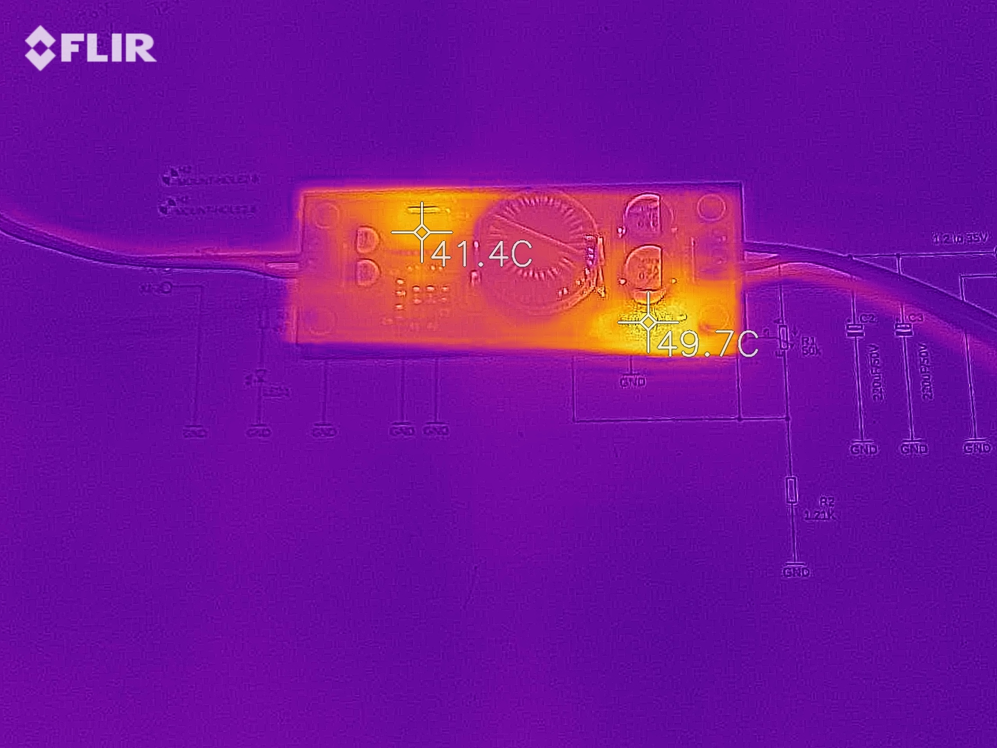
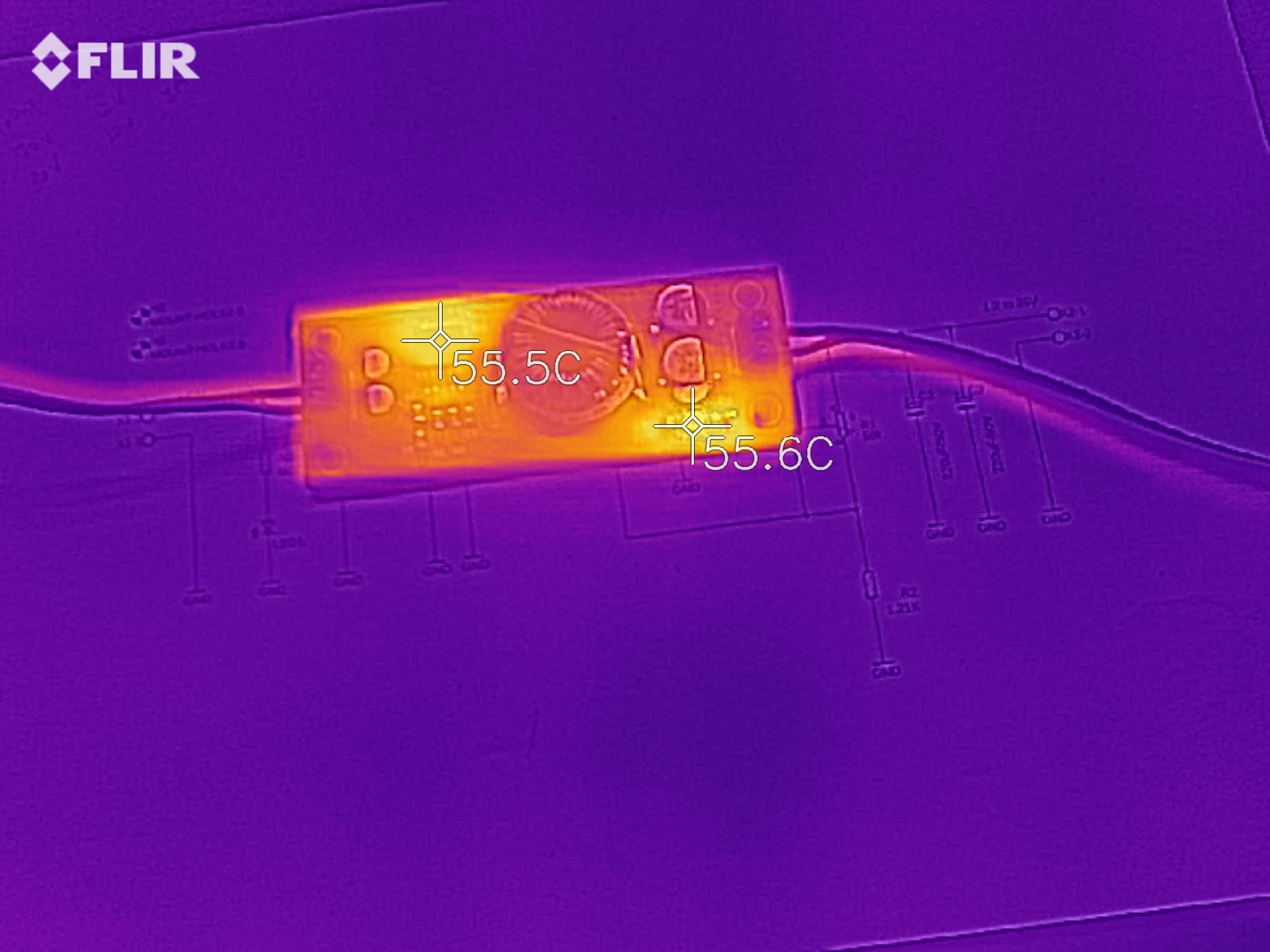
At maximum output power, there is significant heat produced by IC1 and for that reason, we mounted it directly on the ground plane to achieve maximum heat dissipation.
Block Diagram
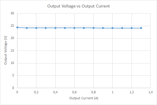
Measurements
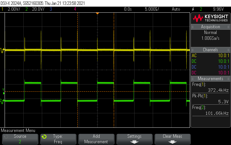
CH1: Output Voltage ripple with 12V Input and 24V @ 500mA output – 5.3 Vpp – CH2: voltage at PIN 4 of IC1CH1: Output Voltage ripple with 12V Input and 24V @ 1A output – 4.6Vpp – CH2: voltage at PIN 4 of IC1
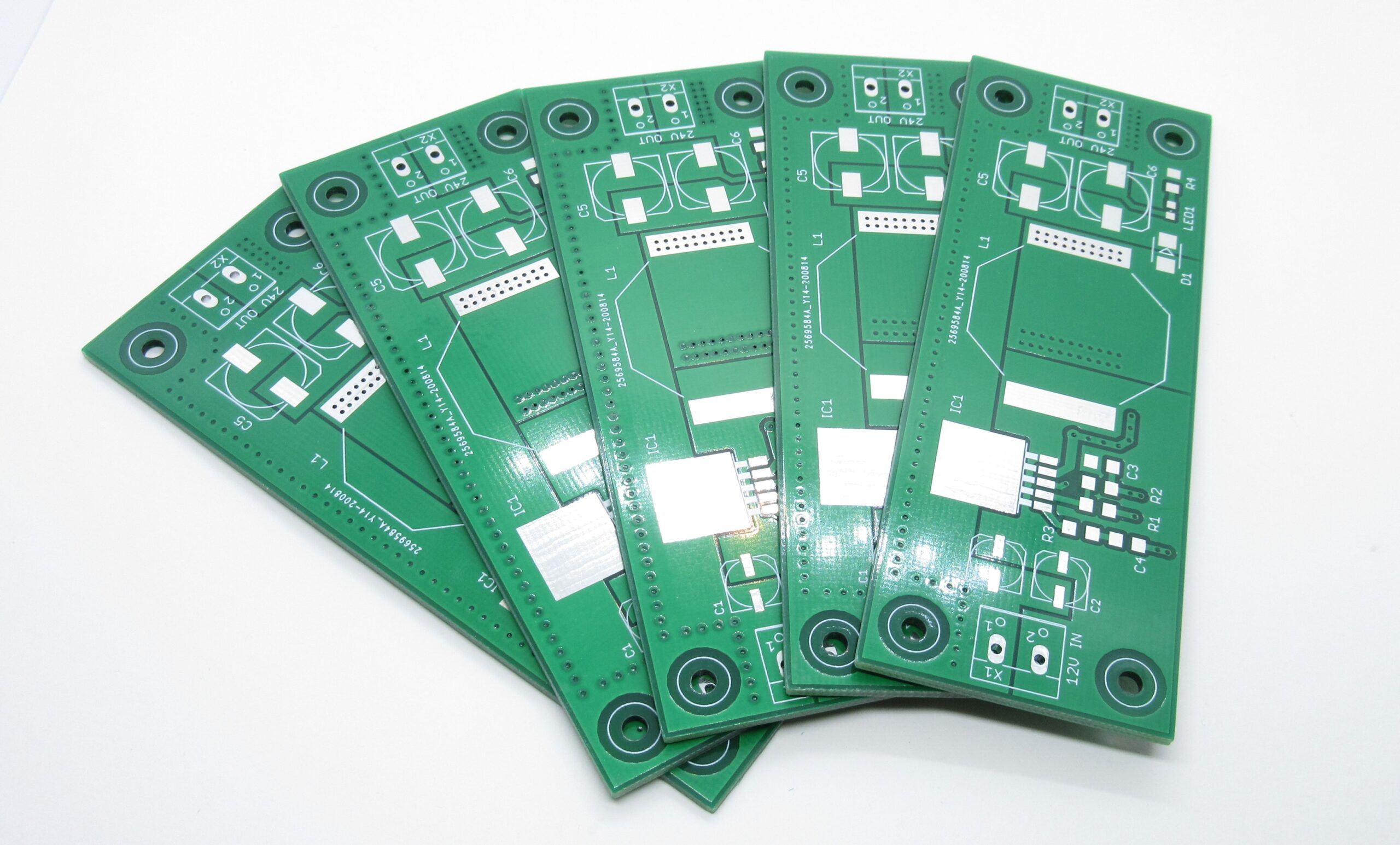
If you would like to receive a PCB, we can ship you one for 6$ (worldwide shipping) click here to contact us
Parts List
Part
Value
Package
MPN
Mouser No
C1 C2
33uF 25V 1Ω
6.3 x 5.4mm
UWX1E330MCL1GB
647-UWX1E330MCL1
C3
0.1uF 50V 0Ω
1206
C1206C104J5RACTU
80-C1206C104J5R
C4
1uF 25V
1206
C1206C105K3RACTU
80-C1206C105K3R
C5 C6
220uF 35V 0.15Ω
10 x 10.2mm
EEE-FC1V221P
667-EEE-FC1V221P
D1
0.45 V 3A 40V Schottky
SMB
B340LB-13-F
621-B340LB-F
IC1
LM2585S-ADJ
TO-263
LM2585S-ADJ/NOPB
926-LM2585S-ADJ/NOPB
L1
120 uH 0.04Ω
30.5 x 25.4 x 22.1 mm
PM2120-121K-RC
542-PM2120-121K-RC
R1
28 KΩ
1206
ERJ-8ENF2802V
667-ERJ-8ENF2802V
R2 R3
1.5 KΩ
1206
ERJ-8ENF1501V
667-ERJ-8ENF1501V
R4
1 KΩ
1206
RT1206FRE07931KL
603-RT1206FRE07931KL
LED1
RED LED 20mA 2.1V
0805
599-0120-007F
645-599-0120-007F
Connections
Gerber View
Simulation
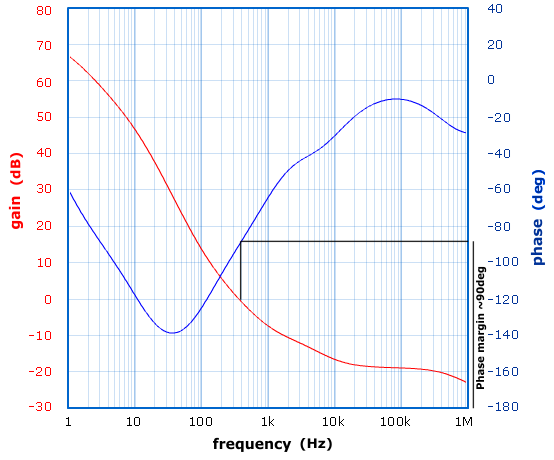
We’ve done a simulation of the LM2585 step-up DC-DC converter using the TI’s WEBENCH online software tools and some of the results are presented here.
The first graph is the open-loop BODE graph. In this graph, we see a plot of GAIN vs FREQUENCY in the range 1Hz – 1M and PHASE vs FREQUENCY in the same range. This plot is useful as it gives us a detailed view of the stability of the loop and thus the stability and performance of our DC-DC converter.
Bode plot of open control loop
What’s interesting on this plot is the “phase margin” and “gain margin“. The gain margin is the gain for -180deg phase shift and phase margin is the phase difference from 180deg for 0db gain as shown in the plot above. For the system to be considered stable there should be enough phase margin (>30deg) for 0db gain or when phase is -180deg the gain should be less than 0db.
On the plot above we see that the phase margin is ~90deg and that ensures that the DC-DC converter will be stable over the measured range.
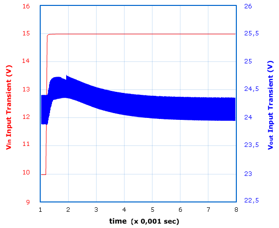
The next simulation graph is the Input Transient plot over time.
Input Transient simulation
In this plot, we see how the output voltage is recovering when the input voltage is stepped from 10V to 15V. We see that 4ms after the input voltage is stepped the output has recovered to the normal output voltage of 24V.
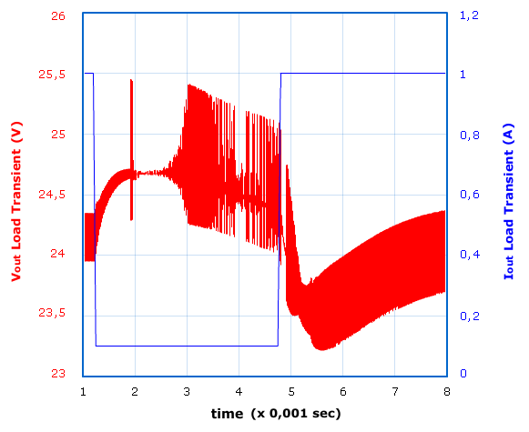
The next graph is the Load Transient.
Load Transient simulation
Load transient is the response of output voltage to sudden changes of load or Iout. We see that the output current suddenly changes from 0,1A to 1A and that the output voltage drops down to 23,2V until it recovers in about 3ms. We also see that when the load is reduced from 1A to 0,1A, output voltage spikes up to ~25,5V, then rings until it recovers to 24V in about 4ms.
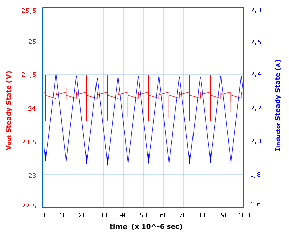
The last graph shows the Steady State operation of DC-DC converter @ 1A output.
This graph shows the simulated output voltage ripple and inductor current. We see that output voltage ripple is ~0,6Vpp and the inductor current has a peak current of 2,4A. The inductor we used is rated at max 5,6A DC so it can easily withstand such operating current and without much heating of the coil.
Operating point data (Vin=13V, Iout=1A)
Operating Values
Pulse Width Modulation (PWM) frequency
Frequency
100 kHz
Continuous or Discontinuous Conduction mode
Mode
Cont
Total Output Power
Pout
24.0 W
Vin operating point
Vin Op
13.00 V
Iout operating point
Iout Op
1.00 A
Operating Point at Vin= 13.00 V,1.00 A
Bode Plot Crossover Frequency, indication of bandwidth of supply
Cross Freq
819 Hz
Steady State PWM Duty Cycle, range limits from 0 to 100
Duty Cycle
48.3 %
Steady State Efficiency
Efficiency
93.2 %
IC Junction Temperature
IC Tj
65.2 °C
IC Junction to Ambient Thermal Resistance
IC ThetaJA
34.9 °C/W
Current Analysis
Input Capacitor RMS ripple current
Cin IRMS
0.14 A
Output Capacitor RMS ripple current
Cout IRMS
0.48 A
Peak Current in IC for Steady State Operating Point
IC Ipk
2.2 A
ICs Maximum rated peak current
IC Ipk Max
3.0 A
Average input current
Iin Avg
2.0 A
Inductor ripple current, peak-to-peak value
L Ipp
0.50 A
Power Dissipation Analysis
Input Capacitor Power Dissipation
Cin Pd
0.01 W
Output Capacitor Power Dissipation
Cout Pd
0.035 W
Diode Power Dissipation
Diode Pd
0.45 W
IC Power Dissipation
IC Pd
1.0 W
Inductor Power Dissipation
L Pd
0.16 W
Configuring Output Voltage
The output voltage is configured by R1, R2 according to the following expression (Vref=1,23V)
VOUT = VREF (1 + R1/R2)
If R2 has a value between 1k and 5k we can use this expression to calculate R1:
R1 = R2 (VOUT/VREF − 1)
For better thermal response and stability it is suggested to use 1% metal film resistors.
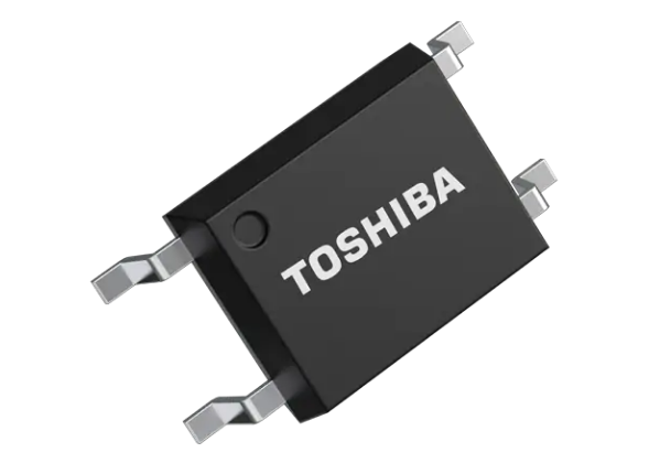
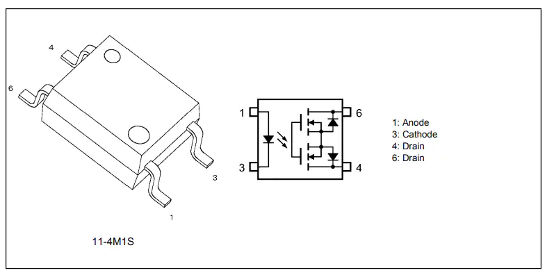
Toshiba Electronic Devices & Storage Corporation has introduced the TLP170AM and TLP170GM two new photorelays that can be used in security systems, which are used in building automation and other industrial equipment.
The TLP170AM has a rated OFF-state output terminal voltage of 60V and constant ON-state current (ION) of 0.7A with the pulse operation of up to 2.1A. The TLP170GM is a 350V version with an ION of 110mA constant current and 330mA pulse operation.
The new photo relays are designed with a maximum trigger LED current of 1mA for reducing the input-side power loss by increasing the sensitivity of the photodiode array. The devices provide lower power consumption and longer operation of devices when they are used in ON/OFF control in battery-powered security devices and various sensors.
The photo relays are packed in 4-pin SO6 Package, this provides a minimum isolation voltage of 3750Vrms allowing the devices to be used in equipment requiring high insulation performance. The new Photorelays are best suitable for security systems, Passive sensors, industrial equipment such as Programmable logic controllers, I/O interfaces, various sensor controls, etc. Building automation systems and in replacement of mechanical relays.
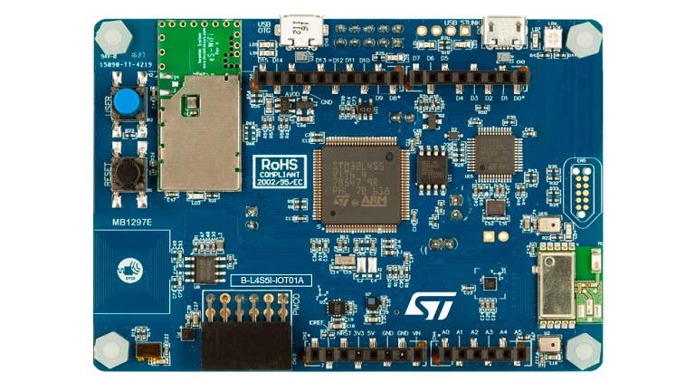
The X-CUBE-AZURE Expansion Package consists of a set of libraries and application examples for STM32L4 Series, STM32F4 Series, and STM32F7 Series microcontrollers acting as end devices.
X-CUBE-AZURE runs on four platforms. The B-L475E-IOT01A and 32F413HDISCOVERY boards support Wi-Fi® connectivity with an on-board Inventek module. The 32F769IDISCOVERY board provides a native Ethernet interface. The P-L496G-CELL02 pack includes an STM32L496AGI6-based low-power Discovery board equipped with Quectel’s BG96 modem (LTE Cat M1/NB/2G fallback) for cellular connectivity.
For the four platforms, a sample application configures the network connectivity parameters, and illustrates the various ways for a device to interact with Microsoft® Azure® IoT Hub. The application shows how a simple client application connects to the Azure® IoT Hub in order to publish device state and telemetry data, and receive device configuration from the cloud.
The application handles Azure® messages, methods and twin update commands. This allows, from the Azure IoT console, the remote control of the user LED state, the change of the telemetry interval, or the trigger of remote firmware update.
Key features
Ready-to-run firmware example using cellular, Wi-Fi®, and Ethernet connectivity to support quick evaluation and development of Microsoft® Azure® cloud-connected applications
Board configuration interface for connection to the Azure® IoT Hub
Secure Boot and Secure Firmware Update
TLS encryption
Azure® IoT Hub, and bidirectional communication examples implemented
Azure® X509 device authentication and Azure® Device Provisioning Service (DPS)
Connection to an Azure® IoT central demonstration
Connection to STMicroelectronics dashboard for Azure®, for easy sensor data visualization and device control
Specific features on the B-L475E-IOT01A board such as measurement of humidity, temperature, 3-axis magnetic data, 3-axis acceleration, 3-axis gyroscope data, atmospheric pressure, and time-of-flight
It connects to the ST-AZURE-Dashboard for easy sensor data visualization and device control. It is possible to securely update firmware based on a bootloader derived from the X-CUBE-SBSFU Expansion Package.
Device authentication and TLS encryption security features are complemented on the client side by the Secure Boot and Secure Firmware Update features.
The B-L475E-IOT01A board reports telemetry data such as measurement of humidity, temperature, and atmospheric pressure.
If you have developed your prototype on a Raspberry basis and are now looking for an adequate replacement, you will find it in the ND108T from ICP Germany. The industrial PICO-ITX board with only 100x72mm size is delivered with an ARM Cortex A53 processor from the NXP i.MX8M family. Available is a Quad Core and a Dual Core with 1.5GHz as well as three memory sizes of 1GB, 2GB and 4GB LPDDR4 SDRAM with 1600MHz clock rate. The eMMC memory is delivered preloaded with 8Gb, 16GB or 32GB. The ND108T’s memory can be expanded via a Micro SD card slot.
In the basic version, ND108T comes with HDMI 2.0 with 4K resolution, GbE, two USB 3.0, one USB 2.0, one RS-232/422/485, and audio line-out and mic-in. A USB 2.0 OTG or the UART is also available for programming and debugging. In addition to the standard Mini-PCIe with PCIe and USB signal, a Raspberry PI* compatible 40 pin header with GPIO signal is available as an expansion slot. For the 40 pin GPIO interface, the API library is available. If required, the basic version can be upgraded. Dual GbE or other display connectors like LVDS or Display Port are optionally available. The ND108T operates with a 12 Volt power supply in a temperature range of 0°C to 60°C and complies with the CE/FCC Class B standard. Both Yocto and Android are available as Board Support Packages for the ND108T.
*Raspberry Pi is a trademark of the Raspberry Pi Foundation
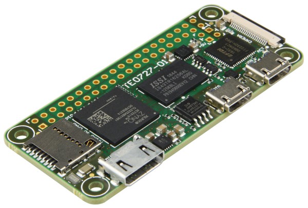
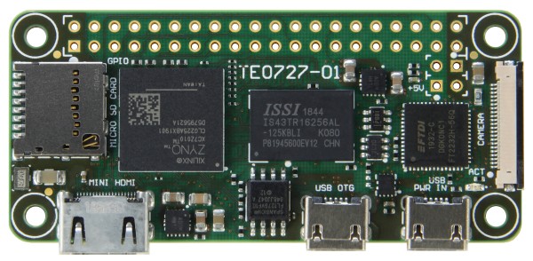
Germany Based Trenz Electronics, has released a new FPGA development board, a 3 x 6.5cm SoC module with integrated Xilinx Zynq-7010 FPGA and a Pi Zero form factor, called the ZynqBerryZero.
The Zyncberryzero
New ZynqBerryZero, nicknamed “little cousin” to older Zynqberry, is the latest addition to the company’s Raspberry Pi inspired FPGA lineup of boards. The ZynqBerryZero is actually raspberry pi-inspired like it’s an older cousin but can be used as an FPGA alternative to the Raspberry Pi Zero.
The ZynqberryZero packs it’s processing power punch with a Xilinx Zynq-7000 FPGA and a dual Arm Cortex-A9 MPCore, physically located in the middle of the FPGA’s programmable logic.
Some features of the ZynqberryZero include:
Xilinx Zynq-7010 FPGA
512 MB DDR3L SDRAM
16 MB flash memory
One microSD card slot
Two microUSB connectors: 1x micro USB for JTAG/UART and 1x micro USB 2.0
40 pin HAT header
Type C mini HDMI connector, and
CSI-2 connector.
Total GPIO: 26 (all provided by high-speed connectors)
Dimensions: 3cm x 6.5 cm
Operating temperature: Depends on customer design and cooling solution.
The ZynqberryZero module is currently available and sells for $149.74 (with shipping) or $129.09 (without shipping). Though the price looks like what could make the ZynqberryZero module quite the investment piece for projects, the module offers users quite a lot of features that make it totally worth it.
The power and flexibility of the FPGA’s capabilities in such a tight, well-designed layout make the ZynqberryZero a great option for a lot of projects. Having an onboard ARM processor surrounded by the programmable logic also means countless design options for the ZynqberryZero module.
The ZynqberryZero can from one of its micro USB ports instead of looking for an external power supply to use.
Displaying the versatility and compatibility features of the ZynqberryZero, Trenz in a recent demonstration showed that with a little tweak, the ZynqberryZero can be used interchangeably with a Pi Zero in projects. This is buttressed by the shared form factor which ensures compatibility with a majority of Raspberry Pi peripherals with little or no adaptation.
A reference design is not currently available for the ZynqberryZero but one can easily work out the pinout based on the available schematics and XDC generator files available on Trenz’s website.
The board is currently available on Trenz’s website for €109.00 excluding shipping. More details on the features and availability of the ZynqberryZero module can be found on the product’s sales page on Trenz’s Online Store.
Earthquakes are shifts or vibrations in the earth’s crust caused by a sudden release of violent energy and the effects that come with them, especially with the large ones, can be devastating. The earlier citizens are warned ahead of its occurrence, the better their chances of survival.
Fair enough, a number of earthquakes early warning systems already exist, but most of these systems are typically centralized and built on expensive equipment. The good news is that Grillo, a distributed sensor expert – in partnership with Linux Foundation and global tech giant, IBM – have open-sourced an IoT-based earthquake early warning system, believed to potentially save lives in the future, called OpenEEW.
Speaking about the origin of the project, Grillo founder, Andres Meira said,
“For years we have seen that EEWs have only been possible with very significant governmental financing, due to the cost of dedicated infrastructure and development of algorithms. We expect that OpenEEW will reduce these barriers and work towards a future where everyone who lives in seismically-active areas can feel safe.”
Speaking also on the OpenEEW being
“the very best in technology and open source”, was Mike Dolan, Senior Vice President and GM of Projects at the Linux Foundation. Dolan said the Linux Foundation is “pleased to be able to host and support such an important project and community”, adding that the OpenEEW project will accelerate the creation of low cost, community-driven projects across the world.
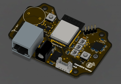
The OpenEEW, by contrast to other EEW systems, can run on a Raspberry Pi single-board computer with a bare-minimum outlay on additional hardware. It is based on low-cost high-performance MEMS accelerometers and is equal with professional seismometers in performance but 60 times less expensive. The sensor also has WiFi and Ethernet connectivity for sending readings back to the central server, a loud buzzer, and 3x bright Neopixel LEDs for alarming. The operating voltage is 3.3V with a current of 1A (maximum).
IBM on its own part, added a new dashboard for the Grillo’s earthquake sensor to visualize sensor readings and thereafter sent out six of the sensor systems to conduct tests in Puerto Rico. The company, through it’s Chief Technology Officer of Call for Code, Daniel Krook, said it will continue to collaborate with Grillo and the Linux Foundation to bring contributions to the openEEW project.
More information on the OpenEEW project including how to deploy your own sensors, detect earthquakes and send alerts, is available on the project’s website and on the project’s GitHub repository.
Arduino, the leading IoT product development platform, has announced it will make security best practices achievable by anyone by including them as standard in the popular, easy-to-use Arduino IoT Cloud solution. Specifically in the IoT space, operating without sophisticated security measures in place can put customers and their data at risk. Today, data, network, and device security remain the primary concern for 50% of organizations when adopting IoT. Arduino understands the risk of compromise and is constantly looking for ways to improve security in both its hardware and software, with a strong focus on “security by design”. Arduino IoT Cloud is a low-code platform that enables users to log, graph, and analyze their sensor data, trigger events, and automate their home or business.
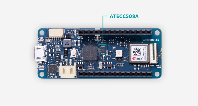
You can sign up for Arduino IoT Cloud for free today and now automatically benefit from integrated security features including: Secure communication with Arduino Portenta H7, Arduino Nano 33 IoT and Arduino MKR family boards using their on-board secure elements (NXP EdgeLock SE050 or Microchip ATECCX08A) The open-source ArduinoBearSSL library for implementing the TLS protocol on devices A device certificate provisioning process to allow client authentication during MQTT sessions.
Fabio Violante, CEO of Arduino said:
“Our priority has always been to build solutions that ensure maximum security for our users and developers and take every step to minimize risk. We are extremely proud of the development of a model that can make our solutions secure by design. As IoT devices continue to proliferate at pace, we will remain committed to finding even more ways to improve security for years to come.”
Many of today’s embedded devices still do not properly implement the full SSL/TLS stack. Optimized for constrained devices, ArduinoBearSSL aims at producing small code footprints and low RAM usage.
It provides developers with a sturdy foundation to their codebase that is fully interoperable with existing SSL/TLS servers. Security and performance was a focus when fitting the standard Bear SSL into Arduino’s embedded IoT core. Arduino IoT enabled boards to include one or more (as in the case of the Portenta H7) hardware crypto chips dedicated to the fast computation of cryptography operations. RAM is therefore free of these demanding tasks, private keys are stored securely, and true random number generation (a basic operation to ensure secure communications) can be delivered effectively.
Different communication techniques are put in motion behind the scenes to guarantee a point to point encrypted communication between the Arduino-powered IoT device and Arduino’s servers. Both techniques, asymmetric and symmetric encryption, facilitate a handshake between the client and the server, and issuing unique session keys. The process of device registration in the Arduino IoT Cloud has been simplified to help developers optimize their workflows. Arduino’s API exposes an endpoint a client can interact with, the client requests to register a new device on the Arduino IoT Cloud, to which the server (API) returns a UUID (Universally Unique IDentifier) that will be stored in the board’s crypto element. From that moment and on, developers can use that UUID in their code to identify their devices against the Arduino IoT Cloud. The device’s private key cannot be extracted by the secure element – a fundamental benefit of installing the IoT Cloud security model on official Arduino boards.
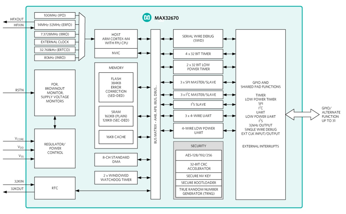
In the Darwin family, the MAX32670 is an ultra-low power, cost-effective, high reliability 32-bit microcontroller enabling designs with complex sensor processing without compromising battery life. It combines a flexible and versatile power management unit with the powerful Arm® Cortex®-M4 processor with floating point unit (FPU). The MAX32670 also offers legacy designs an easy and cost optimal upgrade path from 8- or 16-bit microcontrollers.
The device integrates up to 384KB of flash and 160KB of SRAM to accommodate application and sensor code. error correction coding (ECC), capable of single error correction and double error detection (SEC-DED), is implemented over the entire flash, RAM, and cache to ensure ultra-reliable code execution for demanding applications. Additional features such as the two windowed watchdog timers with fully flexible and independent clocking have been added to further enhance reliable operation. Brownout detection ensures proper operation during power-down and power-up events and unexpected supply transients.
Multiple high-speed peripherals such as 3.4MHz I²C, 50MHz SPI, and 4MBAUD UARTs are included to maximize communication bandwidth. In addition, a low-power UART is available for operation in the lowest power sleep modes to facilitate wakeup on activity without any loss of data. A total of six timers with I/O capability are provided, including two low-power timers to enable pulse counting, capture/compare and PWM generation even in the lowest power sleep modes. The device packs all this capability in tiny form factors: 5mm x 5mm 40-pin TQFN-EP and 1.7mm x 2.2mm 24-bump WLP packages.
Key features
High-Efficiency Microcontroller for Low Power, High Reliability Devices
Arm Cortex-M4 Core with FPU Up to 100MHz
384KB Flash Memory with Error Correction
160KB SRAM (128KB with ECC Enabled), Optionally Preserved in Lowest Power Modes
16KB Unified Cache with ECC
UART Bootloader
Dual or Single-Supply Operation
Ultra-Low 0.9–1.1V VCORE Supply Voltage
Internal LDO Operation from Single Supply 1.7V to 3.6V
Wide Operating Temperature: -40°C to +105°C
Flexible Clocking Schemes
Internal High Speed 100MHz Oscillator
Internal Low Power 7.3728MHz and Ultra-Low Power 80kHz Oscillators
14MHz to 32MHz Oscillator (External Crystal Required)
32.768kHz Oscillator (External Crystal Required)
External Clock Input for the Core
External Clock Input for the LPUART and LPTMR
Power Management Maximizes Uptime for Battery Applications
44µA/MHz Active at 0.9V Up to 12MHz
50µA/MHz Active at 1.1V Up to 100MHz
2.6µA Full Memory Retention Power in Backup Mode at VDD = 1.8V