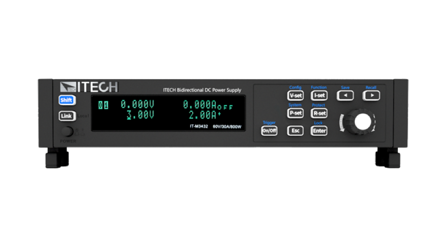
Released by ITECH in March 2020, the brand new series IT-M3400 Bidirectional DC Power Supply comes with cutting-edge technology which is integrated with engineers’ innovative inspiration. It integrates the features of a bidirectional power supply and a regenerative load. Meanwhile, it is also eco-friendly, helps to eliminate the heat dissipation to a minimum level and save your cost as well. IT-M3400 can fully contribute to environmental protection by reducing CO2 emissions.
The compact ITECH M series, ½ wide 19″rack module of 1U high, are available in four different voltage ranges (0-60V, 150V, 300V and 600V) at power ratings of 200W, 400W and 800W.
The full range of models supports multiple units stacking and parallel connection by easy design “legs” plug-in. Fit with rack mount kit to achieve the perfect use.
SOURCING & SINKING
The most important feature of the ITECH IT-M3400 Ultra Compact Bi-directional DC power supplies is the integration of the functionality of a bi-directional power supply and a regenerative electronic load. The unit automatically switches between power supply and load at lightning speed according to the circumstances, without overshooting current and voltage. Its regenerative character also makes the IT-3400 an enormously efficient power supply. The absorbed DC power is converted to AC and fed back into the grid with an efficiency of 90%. As a result, considerable savings can be made on air conditioning and electricity costs.
SIMULATE AND TEST BATTERY CELLS
With the standard software it is possible to easily charge and discharge the battery. With the extensive ITS5300 software you can also perform extensive drive cycle testing, life cycle testing, IR testing etc. In cooperation with the extensive BSS2000 battery simulation software, the IT-M3400 power supply is ideal for simulating battery modules. Specific properties of the battery can be programmed and thus the electronics around the battery can be tested. The specific battery conditions are then very easy to simulate.
MULTI CHANNEL ATS SYSTEMS
Thanks to the ability to connect different IT-M3400 power supplies in parallel, a wide power range can be covered. Also, up to 16 channels can be controlled independently or synchronously with a single interface. The compact design makes the IT-M3400 an excellent candidate for installation in automatic test systems to perform multi-channel tests. Ideal for large-scale testing of power electronics such as IGBT Power Modules or bi-directional DC/DC converters commonly used in electric vehicles. The IT-M3400 series is available with common I/O interfaces and compatible with most communication protocols.
Besides, IT-M family includes IT-M3100 Ultra-compact Wide Range DC Power Supply, IT-M3200 High Precision Programmable DC Power Supply, IT-M3300 Regenerative DC Electronic Load, IT-M3600 Regenerative Power System, IT-M7700 Programmable AC Power Supply. Learn more about ITECH products and solutions, please visit https://www.itechate.com
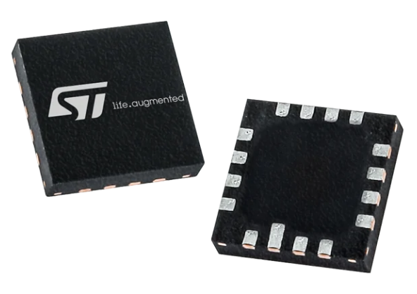
STMicroelectronics’ high-accuracy and low-power two-axis linear accelerometer includes digital output.
The STMicroelectronics IIS2ICLX is a high-accuracy (ultra-low noise, high stability and repeatability) and low-power two-axis linear accelerometer with digital output. The IIS2ICLX has a selectable full scale of ±0.5/±1/±2/±3 g and is capable of providing the measured accelerations to the application over an I²C or SPI digital interface. Its high accuracy, stability over temperature and repeatability make IIS2ICLX particularly suitable for inclination measurement applications (inclinometers).
The sensing element is manufactured using a dedicated micromachining process developed by STMicroelectronics to produce inertial sensors and actuators on silicon wafers. The IC interface is manufactured using a CMOS process that allows a high level of integration to design a dedicated circuit which is trimmed to better match the characteristics of the sensing element. The IIS2ICLX has an unmatched set of embedded features (programmable FSM, Machine Learning Core, sensor hub, FIFO, event decoding, and interrupts) which are enablers for implementing smart and complex sensor nodes that deliver high accuracy and performance at very low power.
Features
2-axis linear accelerometer
Selectable full scale: ±0.5/±1/±2/±3 g
Ultra-low noise performance: 15 µg/√Hz
Superior stability over temperature (<0.075 mg/°C) and repeatability
Embedded compensation for high stability over temperature
I²C/SPI digital output interface
Low power: 0.42 mA with 2 axes delivering full performance
Sensor hub feature to efficiently collect data from additional external sensors
Smart embedded FIFO up to 3 kbytes
Programmable high-pass and low-pass digital filters
Programmable Machine Learning Core to integrate AI algorithms and reduce power consumption at system level
Programmable Finite State Machine to process data from accelerometer and one external sensor
Extended operating temperature range (-40°C to +105°C)
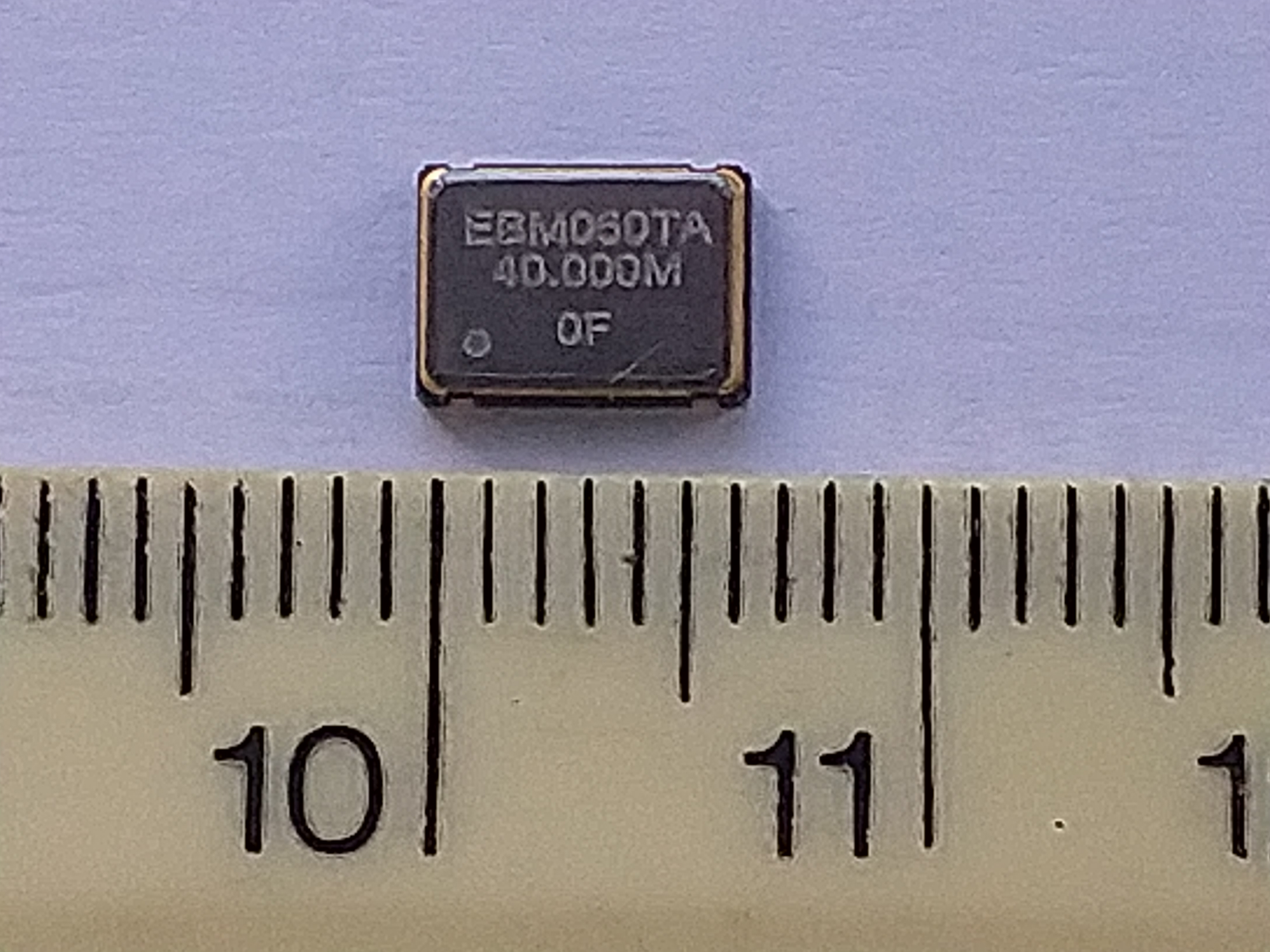
The EQXO-75UIE series is a ruggedized high-reliability, high temperature range clock oscillator in a standard format 7x5mm SMD ceramic package designed for demanding and vibrating industrial applications
Saelig Company, Inc. has launched the Euroquartz EQXO-75UIE Extended Industrial Temperature Ruggedized High-Reliability Oscillators. The EQXO-75UIE series is a ruggedized high-reliability SMD clock oscillator. Designed for demanding industrial applications, it provides reliable operation with excellent frequency stability across an extended industrial operating temp range of -40degC to +105degC. Mechanical shock survivability has been tested to 1500G MIL-STD-883K Meth 2002.5, Condition B. Temperature stabilities of ±50, 75 & 100ppm are available, with tighter options by request (dependent on conditions). This component, available with short lead time, has no ITAR restrictions. All EQXO-75UIE crystals are pre-aged as part of an additional manufacturing process in order to improve long-term application stability. With an aging specification of ±1ppm maximum for the first year, an even tighter aging specification is available by request.
EQXO-75UIE SeriesFeatures
Frequency Range: 2.00MHz to 60.00MHz
Operating Temperature: -40degC to 105degC
Shock Survivability: 1500G
Supply Voltages: 2.5V, 3.3V and 5V
Crystal Stabilization: 96 hours at 100degC
ITAR Restriction: none
If phase noise is a critical project design consideration then it is important to realize that vibration causes a degradation in both spectral output and phase noise. Even moderate levels of vibration can significantly introduce an unwanted signal variation. The acceleration-sensitivity (“g-sensitivity”) of components is often a limiting factor in these applications, and quartz crystals often prove to be a critical limiting component in a design.
The EQXO-75UIE Series of ruggedized, high-reliability, high temperature clock oscillators are made by European frequency product specialist Euroquartz, an independent UK-based manufacturer and supplier of quartz crystals, oscillators, filters and frequency-related products to the worldwide electronics industry. The company is AS9100 registered and designs and manufactures a comprehensive range of frequency control components for a wide range of customers for military and aerospace, communications, general electronics, computing, control systems and petrochemical applications. The EQXO-75UIE Series is available now from Euroquartz’ USA technical distributor Saelig Company, Inc.
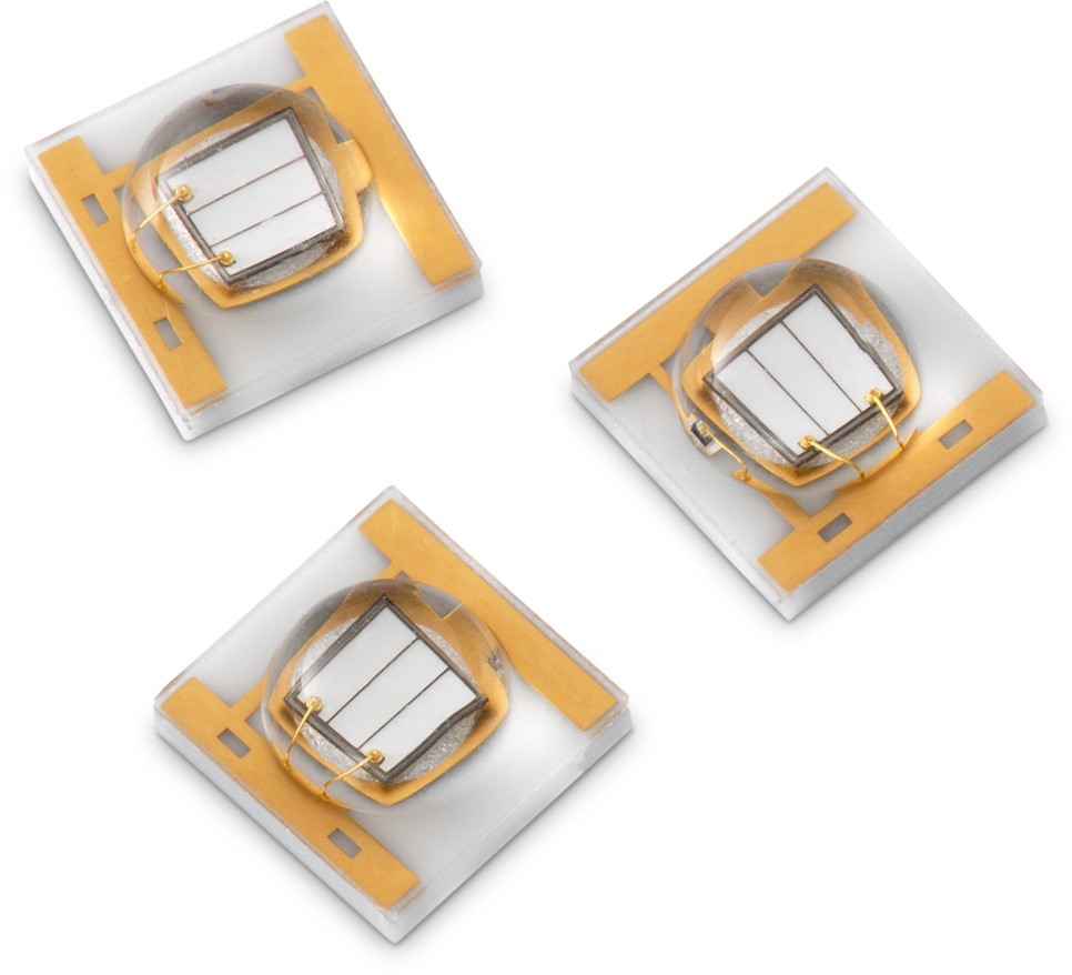
Würth Elektronik High Power Ultraviolet LEDs deliver high intensity UV output in a compact, industry-standard, 3535 ceramic package. Available with 385nm, 395nm, and 405nm peak outputs, these LEDs are an ideal choice for UV systems for curing, printing, and adhesive coating. These LEDs can also be used for high current applications such as special lighting, counterfeit detection systems, and security forensics tools. Würth Elektronik UV LEDs are a perfect upgrade from traditional mercury-vapor (Hg) lamps in these applications, offering faster turn-on time, higher power output, and a longer lifetime.
In the introduction tutorial Operational Amplifier Basics, we have briefly seen that from the same op-amp, many configurations leading to different functions can be adopted, depending on how the feedback loop is designed.
In this new tutorial, we propose to detail the most common configurations along with their function.
We chose to group the configurations in three distinct major groups which will constitute the sections of this tutorial. The first section will, therefore, focus on the buffer designs,
The second section presents the amplifier configurations whose goal is to amplify a signal. Finally, the third section presents the operational op-amps which transform one or more signals to perform elementary mathematical operations.
Buffer configurations
A buffer amplifier is a block that is placed between two circuits which impedances are not matching: a high (resp. low) output impedance connected to a low (resp. high) input impedance. The goal of the buffer is to insulate the stages from each other and perform an impedance adaptation.
Since our tutorial concerns op-amps, we will only talk about voltage buffers but there are also current buffers.
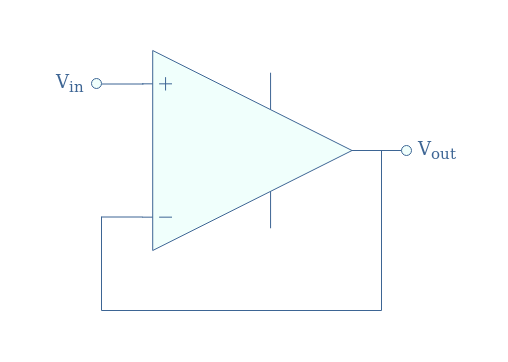
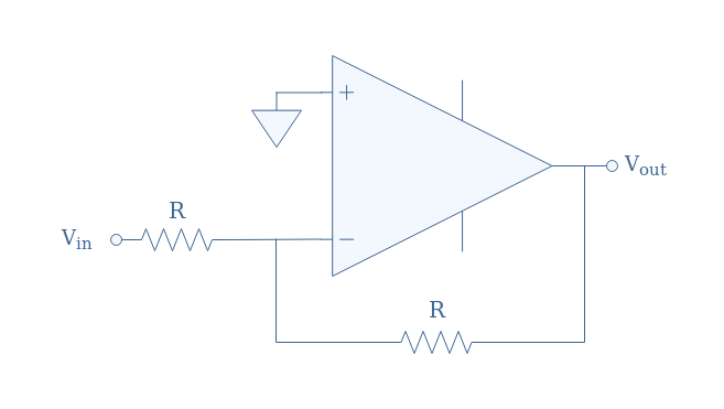
Voltage follower
The voltage follower is a buffer that does not amplify nor inverts the signal. Consequently, its gain is equal to +1. The design of the voltage follower is very simple and simply consist of a short-circuit feedback to the inverting input (-) of the op-amp:
fig 1: Voltage follower circuit
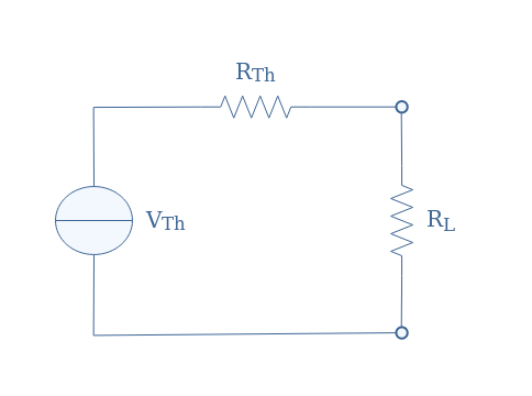
In order to really understand the purpose of this circuit, consider a Thevenin sourceVThwith an internal series resistance RTh that supplies an output load RL such as shown in Figure2:
fig 2: Thevenin source driving a load
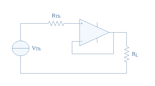
Due to the voltage division phenomenon, the source (VTh, RTh) will only be able able to provide a voltage VThRL/(RL+RTh) to the load. Let’s now place a voltage follower circuit between the source and the load:
fig 3: Voltage follower in a Thevenin circuit
If we label Zin the input impedance of the op-amp, the voltage provided to the amplifier is Vin=VThZin/(Zin+RTh). However, since the input op-amp impedance is very high (Zin>>RTh), or even infinite if we consider the amplifier to be ideal, the input voltage in the op-amp can actually be simplified to Vin=VTh.
Since the voltage follower has a gain of +1, the output voltage is Vout=VTh. The voltage provided to the load can be written VThRL/(RL+Zout), however, the output impedance (Zout) of an op-amp is very low (Zout<<RL) or even equal to zero if we consider the op-amp to be ideal. As a consequence, the voltage provided to the load can be simplified to VTh.
In that example, we can see that the voltage VTh is entirely provided to the output load without any division phenomena thanks to the voltage follower. The circuit shown in Figure 3 actually acts as an ideal voltage source with zero Thevenin internal resistance.
Inverting buffer
If we consider the circuit in Figure 1, add resistors in the feedback loop and inverting input, and connect the non-inverting input to the ground, we obtain a circuit known as inverting buffer:
fig 4: Inverting buffer circuit
Assuming that the value of the resistors is strictly identical under the working condition of the op-amp, the gain of this circuit is -1. The signal is therefore not amplified but inverted: Vout=-Vin.
Amplifier configurations
In this section, we present some configurations for which the op-amp act as an amplification device, meaning that Vout>Vin.
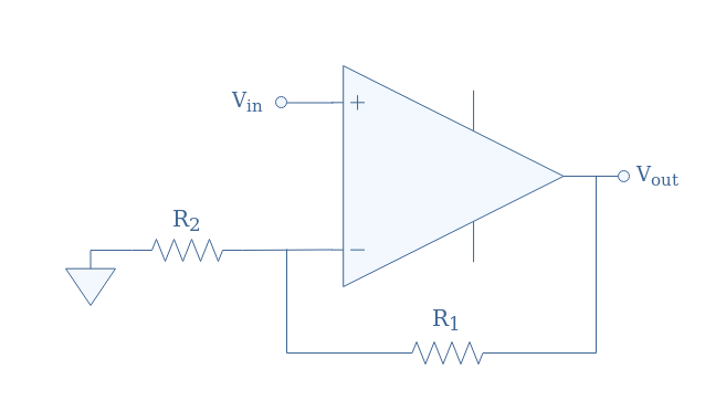
Non-inverting amplifier
We consider a similar circuit to the one presented in Figure 4, the resistors are, however, not necessarily of similar value and the input signal is provided to the non-inverting input (+):
fig 5: Non-inverting amplifier circuit
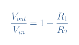
The gain Vout/Vin of the non-inverting amplifier is always strictly higher than +1 and given by Equation 1:
eq 1: Non-inverting amplifier gain
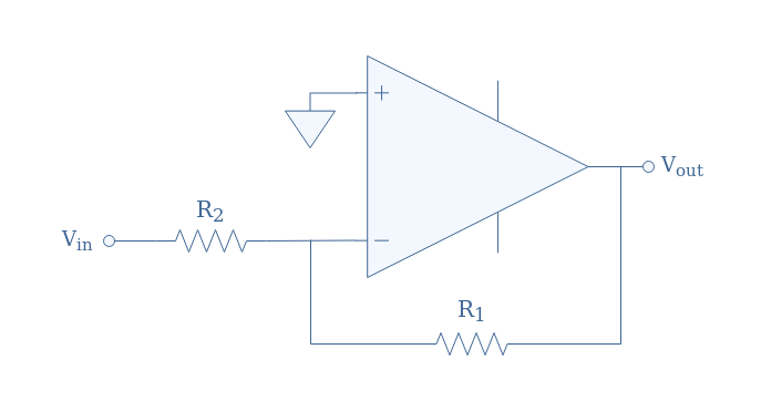
Inverting amplifier
The inverting amplifier is designed by grounding the non-inverting input and applying the signal to the inverting input in the circuit presented in Figure 5.
fig 6: Inverting amplifier circuit
The gain is given here by the ratio -R1/R2, the negative sign assures that the signal is inverted.
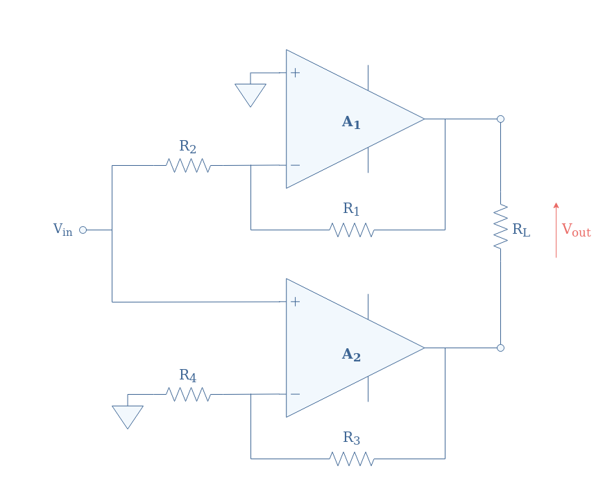
Bridge amplifier
An inverting and non-inverting amplifier can be connected together to form a bridge amplifier. In this circuit, the input is common to both amplifiers while the output is taken on a load RL that is connected between the outputs of the amplifiers.
fig 7: Bridge amplifier circuit
According to the previous subsections, the output of the first amplifier will be A1Vin with A1=-R1/R2. The output of the non-inverting amplifier is A2Vin with A2=1+(R3/R4).
Finally, with the direction convention chosen for Vout, the output of the bridge amplifier is given by (A1-A2)Vin. We can note that if the resistors are appropriately chosen, the magnitudes of the gain can be equalized (|A1|=|A2|), which allows the bridge amplifier to increase by a factor 2 the maximal amplification that a single amplifier could perform.
The advantage of the bridge amplifier is to be able to supply more power to an output load, by a factor 4. Moreover, a single-supply is able to drive both amplifiers that constitute the bridge amplifier, thus simplifying the design and cost of the circuit.
Operational configurations
Some op-amps configurations can perform elementary mathematical operations. In the following, we present the adder/subtractor and the derivator/integrator circuits.
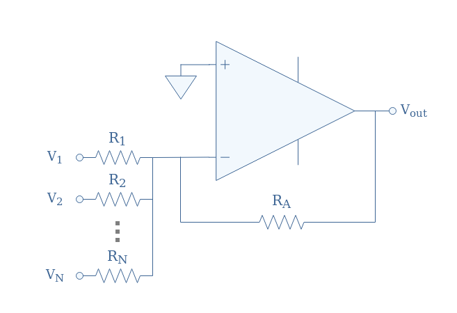
Adder/subtractor
The adder configuration takes several voltages on its inverting input connected via resistors.
fig 8: Adder circuit with N inputs
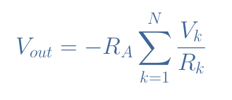
In the general case, the voltage Vout satisfies Equation 2:
eq 2: Adder configuration formula
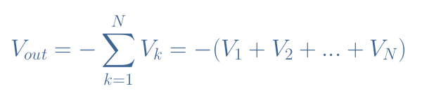
It is interesting to equalize all the resistances RA=R1=…=RN, which leads to a simplified formula where we can clearly see that the configuration presented in Figure 8 effectively adds the voltages:
eq 3: Simplified adder configuration formula
Note that the presence of the minus sign means that the voltage sum is inverted. In order to add the voltages without an inversion, we can simply place an inverting buffer after this stage.
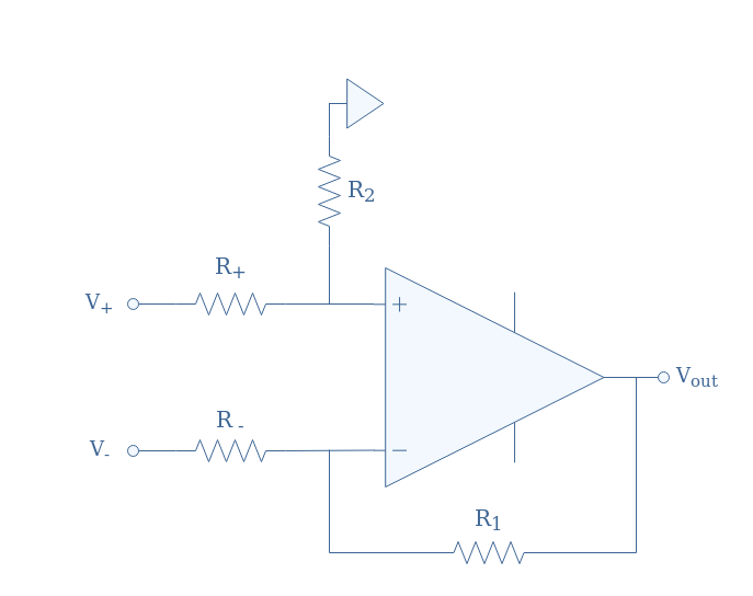
To realize a subtractor configuration, both the inverting and non-inverting output are used such as shown in Figure 9:
fig 9: Subtractor circuit
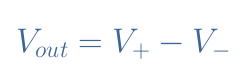
The configurations become again interesting when the resistor values are appropriately chosen so that R–=R1 and R+=R2. In that case, the subtractor function can be performed:
eq 4: Subtractor configuration formula when R–=R1 and R+=R2
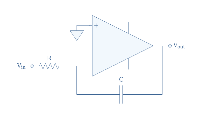
Derivator/Integrator
We start with the derivator which input is connected via a capacitor to the inverting branch, the feedback loop is connected with a resistor:
fig 10: Derivator circuit
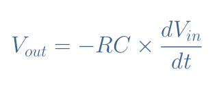
The output is proportional to the variations of the input signal given by the derivative function:
eq 5: Derivator configuration formula
Derivators are useful to control the variations of certain physical parameters previously transformed in an electrical signal such as the temperature, pressure…
By inverting the position of the capacitor and resistor in Figure 10, we obtain the circuit of an integrator:
fig 11: Integrator circuit
For this circuit, the output is proportional to the integral of the input:
eq 6: Integrator configuration formula
Conclusion
We have presented in this tutorial some of the most important building blocks that can be realized with operational amplifiers. We chose to distinct these configurations in three groups depending on their function.
In the first section, we focused on the buffer configurations which do not amplify or modify the signal. The buffers can either be non-inverting (Vout=Vin) or inverting (Vout=-Vin) depending on which input the signal is applied. Thanks to their high input and low output impedances, buffers are mainly used to connect unmatching circuits together.
Amplifier configurations are presented in the second section with again, a distinction being made between inverting and non-inverting amplifiers. In both cases, it is the values of the resistors connected to the inverting branch that will dictate how much the output signal will be amplified. To conclude this section, we have presented the bridge amplifier which consists of interconnecting an inverting and non-inverting amplifier in order to increase the power that can be supplied to the output load.
Finally, operational configurations that can perform elementary mathematical operations are presented in the last section. An adder amplifier can be realized with an inverting op-amp with multiples inputs, a subtractor is realized with inputs on both inverting and non-inverting inputs. In both cases, it is interesting to equalize the resistors present in the circuit in order to realize additions and subtractions with any prefactor. Moreover, integrator and derivator designs are presented, they both have a capacitor in their design and are used either to integrate or derivate the input signal, these functions are widely used in automation.
AAEON and AOTU.AI are excited to announce the launch of the BrainFrame Edge AI Developers Kit (DevKit) on an Intel AI platform for IoT that will allow developers and system integrators to rapidly create and deploy Smart Vision applications.
AI computer (smart) vision applications are often bespoke and laborious to build and deploy. The BrainFrame Edge AI DevKit provides a new paradigm in creating solutions such as vision-based access control, uniform compliance, manufacturing automation, and video analytics.
AAEON’s fanless industrial computer is powered by 8th Generation Intel® Core™ i5 Processors and Intel® Movidius™ Myriad™ X VPU and pre-installed with the Aotu.ai BrainFrame™ Smart Vision platform.
BrainFrame™ is a platform designed to be easy to scale and highly configurable to allow any connected camera to become a continuously monitoring Smart Vision system. BrainFrame’s automatic algorithm fusion and optimization engine is powered by VisionCapsules™, Aotu.ai’s open source algorithm packaging format. These self-contained capsules have a negligible memory footprint and include all necessary code, files, and metadata to describe and implement a machine learning algorithm.
VisionCapsules enable drag and drop Smart Vision AI algorithms and provides complete support for the Intel Distribution of OpenVINO™ toolkit. The deep integration of the OpenVINO toolkit fully leverages the optimization and acceleration offered by the toolkit on Intel’s processors.
Stephen Li, CEO of Aotu.ai, explains,
“we built BrainFrame when we saw how fragmented the Smart Vision AI ecosystem is and how complex it was to create and deploy a system. We realized there is an opportunity for a platform that can become the “Android OS” of video cameras where you can download algorithms as easy as downloading Android applications.”
“With Intel’s 8th Generation Core processors and Myriad X VPU, the DevKit provides outstanding performance and value for developers needing the computational power for their applications,” said Jason Lu, Product Manager with AAEON North America. “Paired with Aotu.ai’s BrainFrame provides for immense expandability and support for AI applications, while removing unnecessary complexities during the development process.”
“AI is transforming the IT industry, and Smart Vision is one of the leading drivers of that transformation. The Aotu.ai and Aaeon solution on Intel’s platform is operationalizing and accelerating the deployment of AI-based Smart Vision in the ecosystem.” said Dr. Cormac S.G. Conroy, Board Member, Aotu.ai.
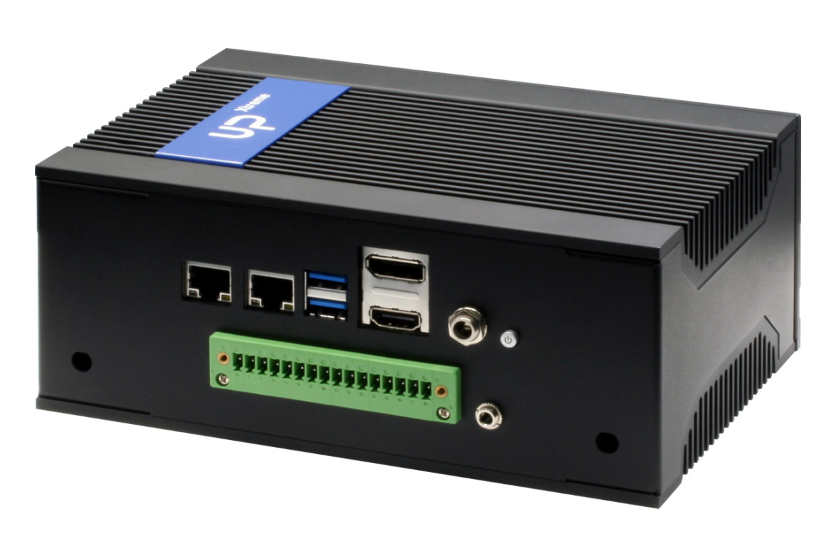
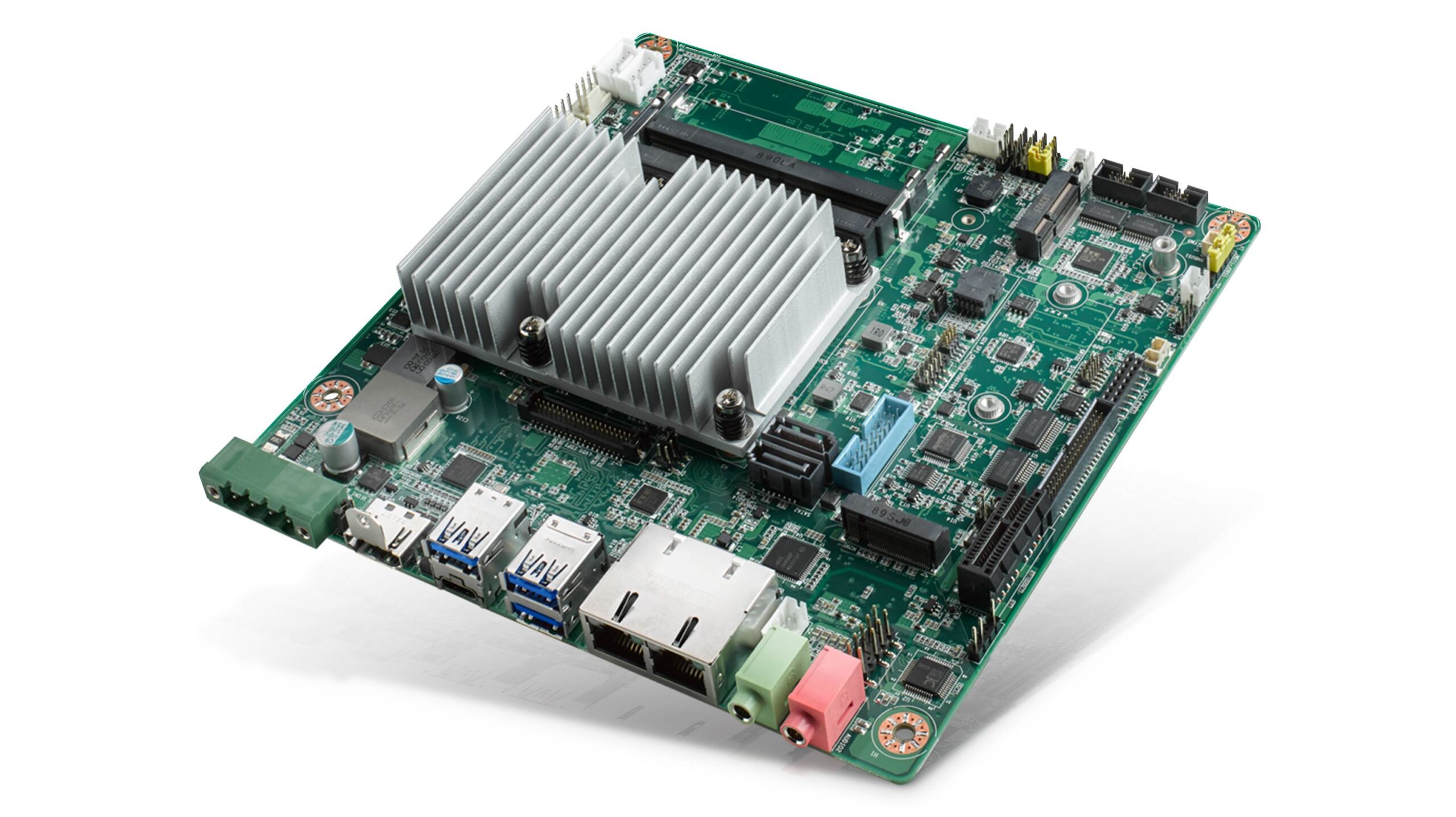
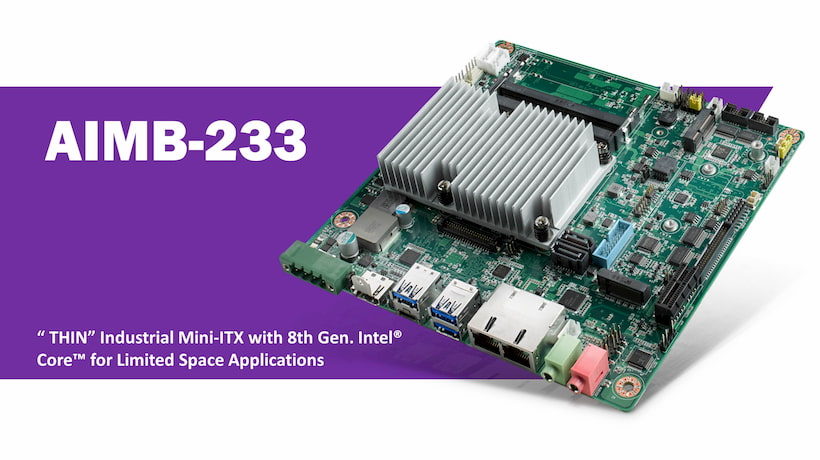
Advantech, a leading industrial solutions provider, is pleased to release AIMB-233, a low-profile industrial-grade “THIN” Mini-ITX motherboard to enable graphics processing and computing power in limited space applications. AIMB-233 is powered by an 8th Gen. Intel® Core™ Processor, features diverse I/O ports, and utilizes an optimized thermal solution. With an overall height of just 25 mm (.08 in), this motherboard is an excellent choice for applications in nursing carts, patient care systems, Human-Machine Interfaces (HMI), and mobile devices.
Featuring Dual Ethernet and Numerous I/O for Diverse Applications
Advantech AIMB-233 features multiple high-speed I/O — including 8 USB ports (1x type C USB 3.1, 3x USB 3.1, 2x USB 3.0, 2x USB 2.0), 2x SATA III, PCIe x1, 1x M.2 M-Key, and 1x M.2 E-key (optional full-size MiniPCIe) — to consolidate legacy and modern peripheral devices on a motherboard. Additionally, this motherboard has 8-bit digital programmable I/O, 6x COM ports (one port for RS-232/422/485), and a 2W dual-channel audio amplifier. AIMB-233 is further equipped with dual Gigabit Ethernet ports that deliver up to 1000 Mbps of bandwidth for two network segment applications. These features allow AIMB-233 to support a wide range of peripherals and network connections in a myriad of applications.
Designed to Empower High-End Graphics and Low-Latency Storage
AIMB-233 supports high-speed interfaces via USB Type-C Alt to offer USB, DisplayPort and HDMI. USB Type-C Alt supports a max. 4906 x 2034 @60Hz resolution to deliver excellent graphics to medical imaging processing. The M.2 M-key socket enables the use of high-performance SSD to deliver reliable high-speed processing for critical data operations.
Rapid Deployment in Harsh Environments
AIMB-233’s fanless design reduces time-to-market for system integrators. This motherboard provides powerful and stable computing performance during wide temperature range working condition in harsh environments (-20 ~ 70 °C/-4 ~ 158 °F). Additionally, its 12-24V DC-in feature accommodates flexible system power designs for medical and industrial automation applications.
Enhanced Security Solution for Medical Applications
Medical devices, including radiation/diagnostic equipment, monitoring devices, and patient information systems require advanced security capabilities. AIMB-233 motherboard features secure hardware and software to protect data and patient confidentiality. Its software, UEFI Secure Boot and boot guard, secures pre-boot environments, while its hardware supports optional TPM 2.0 for enhanced data protection.
AIMB-233 Key Features
Equipped with 8th Gen. Intel® Core™ i / Celeron mobile processors
Dual channel DDR4-2400 260-pin SODIMM up to 32 GB
8x USB, 2x SATA III, 6x COM, 1x M.2 M-key/8-bit GPIO, 1x M.2 E-key
Triple display by Type C Alt. + HDMI + LVDS (or eDP*)
FCC/CB Class B Certified and ESD level 4 (Contact 8 KV)
12~24V DC power input
Pre-installed WISE-DeviceOn software for remote monitoring and management
*Note: BOM optional function by request.
Advantech AIMB-233 industrial-grade “THIN” Mini-ITX motherboard is available now. For further information or Advantech Industrial Motherboard products, please contact your local sales support team, an authorized channel partner, or visit www.advantech.com.
Next phase of Arduino’s cloud platform enables everyone to breathe digital life into everyday things
ITALY: Arduino, the leading IoT development platform announces the full release of Arduino IoT Cloud – an end-to-end solution that makes building connected projects easy for makers, IoT enthusiasts and professionals from start to finish.
Arduino IoT Cloud provides a low-code approach that enables users to collect, graph and analyze their sensor data, trigger events and fully control their devices. People can automate their home or businesses with ease, all in a single place. Arduino IoT Cloud provides a full stack approach that is ready-to-use, by combining hardware, firmware, cloud services, and knowledge support that is needed to deliver an end-to-end IoT solution. This enables millions of users at any level of experience to start deploying connected projects.
Easy for beginners, fast for professionals
Getting started has never been easier; simply sign up for free today and follow the guides to connect a device to start your project. Arduino IoT Cloud’s low-code approach helps users to optimize their workflows and simplify device registration for convenience and flexibility. For more advanced users, the platform also enables other methods of interaction, including HTTP REST API, MQTT, Command-Line Tools, Javascript, and Websockets.
Arduino IoT Cloud has a range of key features, including:
Automatically generated code that can be easily adapted by users with minimal effort, removing barriers for anyone who is not familiar with coding and empowering makers of all ages and experience Plug & Play onboarding will automatically generate a sketch when setting up a new device, enabling users to go from unboxing their board to a working device within minutes ‘On-the-go’ mobile dashboard allows users to access, check data and control remote sensor monitoring from anywhere using accessible widgets. Using open hardware and IoT standards, users can send and receive data across multiple connected objects within the platform – making it perfectly suited to professionals that want to manage fleets of devices. Arduino IoT Cloud also supports STEM/STEAM learning programs. Educators can share sketches with students with pre-existing code that allows entry-level developers to understand and create projects without having any prior coding experience.
Users can also upgrade their plan to power-up their tools and access additional features. For USD $6.99 per month, the Create Maker plan allows users to connect more ‘things’, save more sketches, increase data storage on the cloud and access unlimited compilation times, plus much more. For businesses, the Create Professional plan provides flexible and scalable options for enterprise solutions.
Complex technology (made simple)
Deploying a connected object with Arduino IoT Cloud requires just a few simple steps by removing the most common points of friction e.g. installing software, security management etc. Arduino IoT Cloud aims to further demystify the set-up, by allowing people to express their requirements in terms of the physical aspects they are trying to capture or influence, for instance temperature, pressure or the status and color of a light, rather than the technical parameters: voltages, currents etc. Users can leverage a wide selection of widgets and assemble them into meaningful dashboards within minutes, by intuitively connecting these UI controls to the physical properties they refer to.
The platform integrates with Amazon Alexa, Google Sheets, IFTTT and ZAPIER, which allows users to program and manage devices using voice, spreadsheets, databases, and automate alerts using webhooks. The platform also enables developers to create custom apps using the Arduino IoT API, with custom endpoint webhooks to be added for further flexibility.
Automatic control of devices through an API puts easy remote management at the heart of the platform. Users can manage, configure and connect not only Arduino hardware, but the vast majority of Linux-based devices, easily and securely through a simple Internet connection. Devices are secured using X.509 certificate-based authentication, with further security benefits unlocked by the secure element crypto chips embedded into Arduino IoT enabled boards.
Fabio Violante, CEO of Arduino commented:
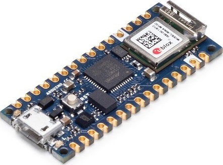
“As technology progresses, things that were impossible to imagine a few years ago are becoming much easier to approach. But when we talk about leveraging the power and robustness of embedded systems to connect physical objects and environments with the cloud, a lot of skills are required. Our aim at Arduino is to lower this barrier to entry for IoT and ultimately, democratize technology. This has been our mission forever, and is why we are investing time, money and energy to build our holistic approach that goes from connected hardware for super secure IoT nodes, like our MKR Wifi 1010 board, Nano 33 IoT or Portenta H7 for the PRO market, to our user friendly cloud and development environments.”
“Especially on the cloud side, our aim is to take care of the “underlying” complexity by performing code generation and automation at every possible step of the process. Combining the ease of build with the ability for users to leverage their mobile device as a control interface through specialized apps for Android and iPhone, we’re excited to make simple and secure IoT possible for everyone.”
The partnership brings 5G-ready NB-IoT over satellite for the first time and delivers massive cost and interoperability advantages for the IoT industry
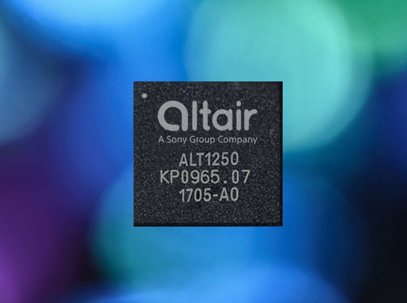
Skylo, maker of the world’s most affordable and ubiquitous network that connects any machine or sensor, today announced a partnership with Sony Semiconductor Israel (Sony, formerly known as Altair Semiconductor). With the partnership, Skylo and Sony are the first to develop and deploy cellular IoT chipsets (branded “Altair”) that can connect via geostationary satellites and that leverage the standardized, 5G-ready, NB-IoT protocol. The partnership also makes significant contributions to 3GPP future specifications, which will help standardize and accelerate the adoption of NB-IoT over satellite. In addition, this innovative new use of Sony’s Altair cellular IoT chipsets dramatically reduces the cost for IoT applications to connect via traditional satellite networks; until the launch of this solution, satellite connectivity was cost-prohibitive and required custom-built protocols.
Skylo, which was founded in late 2017 by foremost researchers including Dr. Andrew Kalman, is building an efficient, global NB-IoT network over satellite for millions of presently unconnected devices, machines, and sensors. Sony Semiconductor Israel is a leading provider of cellular IoT chipsets. Through this partnership, both parties have extended existing cellular IoT chipsets to communicate directly over Skylo’s hosted satellite network.
“For industries with assets deployed all over the globe — including marine vessels, vehicles, and industrial equipment — having access to a ubiquitous fabric of carrier-grade, affordable IoT connectivity that is enabled by Sony’s Altair cellular IoT chipsets is a game-changer,” said Dr. Andrew Nuttall, Skylo’s co-founder, and CTO. “This partnership ensures our ability to quickly scale the manufacturing and deployment of connector Skylo Hubs to our customers worldwide.”
“We are glad to collaborate with Sony Semiconductor Israel on this important technological breakthrough, which provides an entirely new connectivity method for IoT for customers around the world and contributes greatly to the development of future 3GPP standards,” said Moshe Noah, Vice President of Engineering at Skylo.
“We are excited to work with Skylo and launch an entirely new IoT category for industrial machines,” said Dima Feldman, Vice President of Product Management and Marketing at Sony Semiconductor Israel. “We’re impressed by the innovative way that Skylo has extended our chip functionality over satellites to expand the connectivity reach to the most remote locations. We look forward to helping Skylo bring billions of sensors online for the first time.”
“In addition, the Altair field-proven, ultra-low-power, and ultra-small chipset solutions are ideal for the type of data exchange for industrial use cases,” added Feldman.
This new geostationary satellite connectivity is a technological breakthrough for Skylo. Any customer who is building IoT into their remote businesses can use familiar technologies like Bluetooth and WiFi in order to connect existing sensors to Skylo Hub. Those IoT sensors are already programmed for these communications protocols. Adding Skylo’s satellite connectivity is a seamless extension for customers that, in addition to terrestrial networks, can now use satellite connectivity, virtually in any place on the planet. In addition, because Sony’s Altair cellular IoT chipsets are mass-produced for terrestrial cellular networks, Skylo can affordably manufacture the Skylo Hub and pass along that savings to its customers.
Skylo is launching commercially this year over South Asia and can be accessed using the Skylo Hub, a portable satellite NB-IoT antenna terminal. The Skylo Hub costs less than $100 USD and integrates seamlessly with existing machines & sensors. The Skylo Network is hosted on existing geostationary satellites and enables immediate connectivity for customers without the need to add new infrastructure in space. Skylo is venture-backed by leading investors in telecom and space, including SoftBank Group, Boeing HorizonX, Innovation Endeavors, and DCM Ventures.
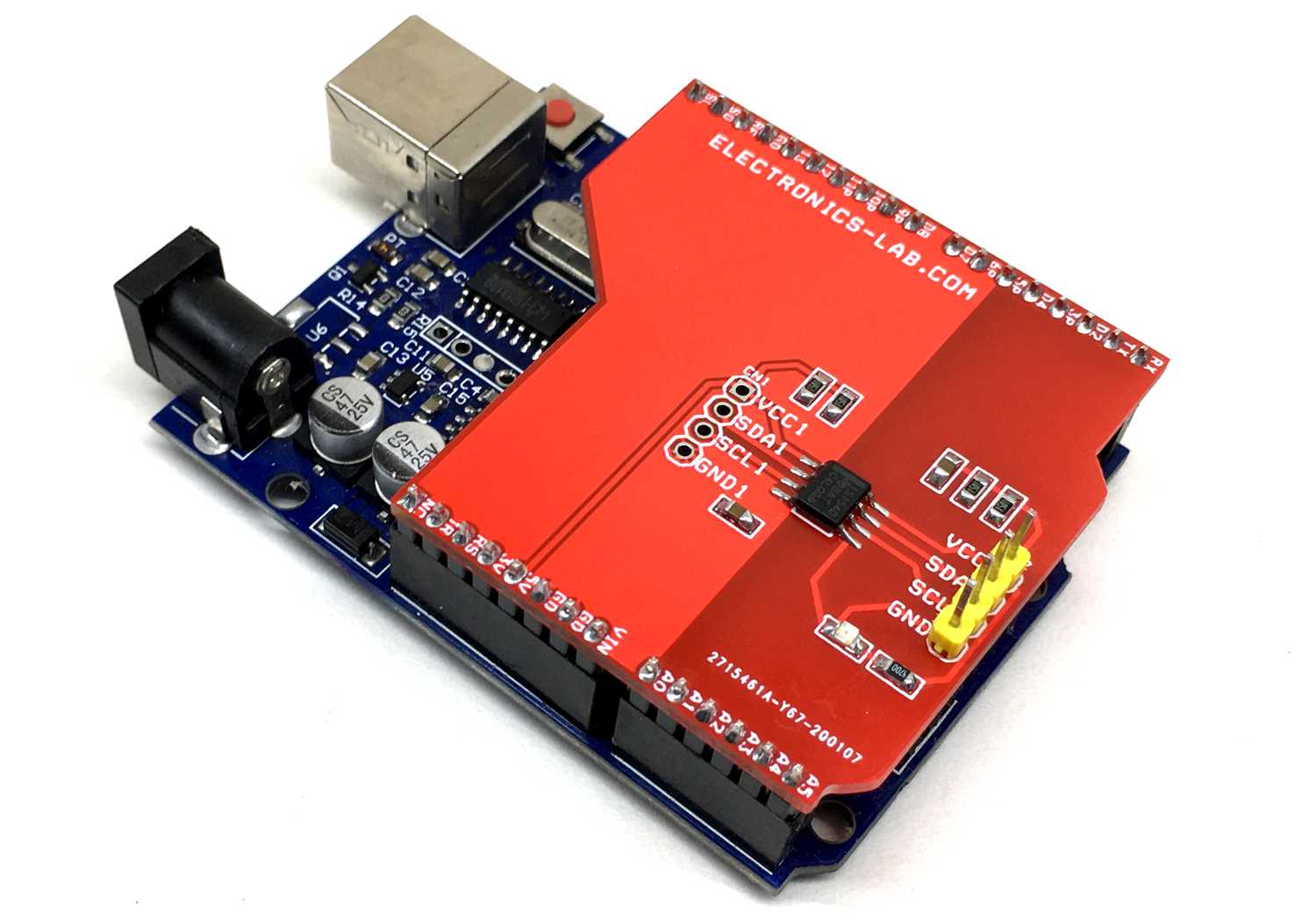
Optically isolator Arduino Shield has been designed to provide optically isolated I2C communication between Arduino and any other device or sensors that works with I2C protocols. I have used the ISO1540 Low-Power Bidirectional I2C Isolator IC from Texas Instruments to build this project, and the device is compatible with I2C interfaces. These devices have logic input and output buffers that are separated by Texas Instruments Capacitive Isolation technology using a silicon dioxide (SiO2) barrier. When used with isolated power supplies, these devices block high voltages, isolate grounds, and prevent noise currents from entering the local ground and interfering with or damaging the Arduino board. The ISO1540 has two isolated bidirectional channels for clock and data lines. The project is suitable for multi-master applications. For applications where clock stretching by the slave is possible. LED D1 is the power indicator for side two. This board requires two separate supplies, side one powered from Arduino UNO 5V, side 2 require separate 3.3V to 5V.
Optically Isolated Bidirectional I2C Shield For Arduino – [Link]