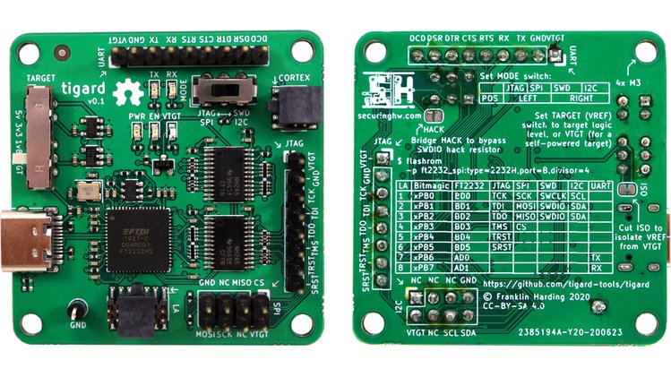
SecurityHardware.com is set to take FT2232H-based USB Serial Adapters and Debuggers to the Next Level. The Portland-based company will soon be launching a Crowdfunding campaign for its latest design, an open-source FTDI FT223H-based multi-protocol, multi-voltage hardware hacking device called Tigard.
Tigard is a one-stop board for developers looking for something a little more than the average USB-UART debugging tool. Speaking on the idea behind the product, the team behind Tigard said
“There are plenty of -232H series breakout boards, but they are generally designed to be an easy way to adapt it to a specific use, and not designed for regularly plugging into all different target systems. The two exceptions are the Exodus Intelligence Hardware Interface Board which is not open hardware or commercially available, and TIMEP which is the origin and heritage of this project.”
the company writes.
Tigard features a rich set of features that places it above and beyond a simple serial adapter. It incorporates commonly used pinouts, logic analyzer connection, onboard level-shifting, and labeled wiring harness, specifically for “attaching to and communicating with low-speed interfaces on reverse-engineered hardware targets.”
The board comes with a USB Type-C connector and is made available under the permissive Creative Commons Attribution-ShareAlike 4.0 license.
A look at some of its hardware features:
Dual serial interfaces; one completely dedicated to UART, with access to flow control signals and the other shared among dedicated headers for SPI, JTAG, I²C and SWD.
Bi-directional level shifters for operations between 1.8 – 5.5V
Power supplier switchable between on-board 1.8, 3.3 and 5.0 V and off-board vTarget supplies
Switch to choose between I²C/SWD and SPI/JTAG operations,
Logic analyzer port to quickly access the device-level signals, and,
Some indicator lights to help in the debugging process
What’s more? Its high compatibility with a number of tools and libraries that already support FTDI’s X232H family-like PySpiFlash, USB-serial drivers, UrJTAG, PyFtdi, OpenOCD, Flashrom, PyI2CFlash, and LibMPSSE. This suggests that the board can be used as a simple serial console, a JTAG debugger, an SPI flash chip dumper or an OLED display driver and analyzer.
More details on Tigard can be found on Crowd Supply. The board is yet to be launched on the Crowdfunding page but you can sign up for updates and notifications when the campaign finally goes live.
The project is open source and all hardware design files, documentation and usage are available on the project’s GitHub repository.
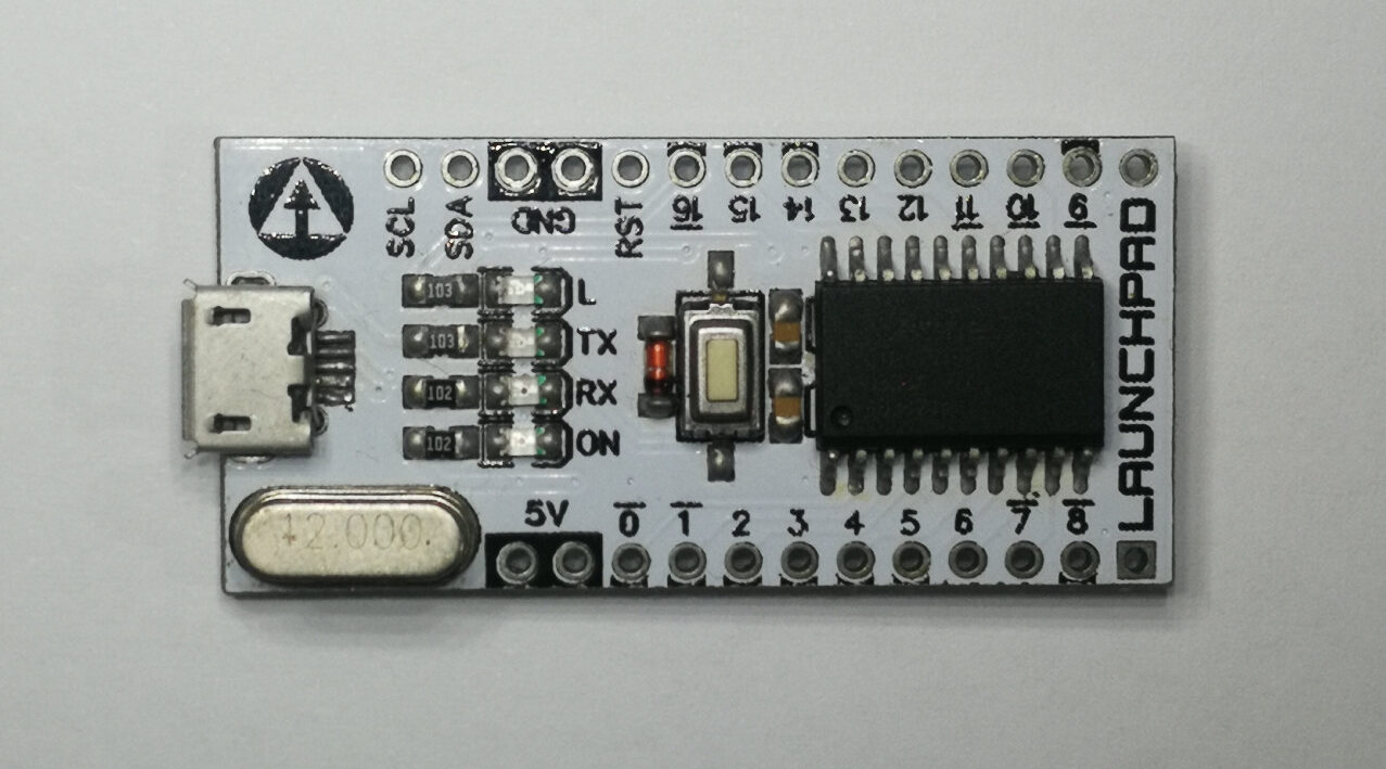
We can’t seem to get enough of Arduino Nano. It has been a “go to” boards for developers since its launch in 2008. We see developers and engineers try to upgrade the Arduino. This has moved Clyde D. Corpuz to launch the Launchpad, which is a small, Arduino compatible microcontroller development board that does away with the old and dated ATmega328p used in the classic Nano in favor of a newer, cheaper, and equally capable AVR microcontroller (currently an ATtiny1616). The goal of this project
“is to design a board aimed at basic education that can be made for as low as $2. The current version has all the features of the classic Nano (albeit fewer pins), plus a faster 20MHz clock speed, and true analog output.”
Also, the project aims to design and create a low-cost (and probably commercially viable) microcontroller development board that is targeted towards both beginners and experts alike; improves upon the Arduino Uno and Nano, and only costs as little as $2 to manufacture. The board should also be intuitive and easy to use for basic education applications.
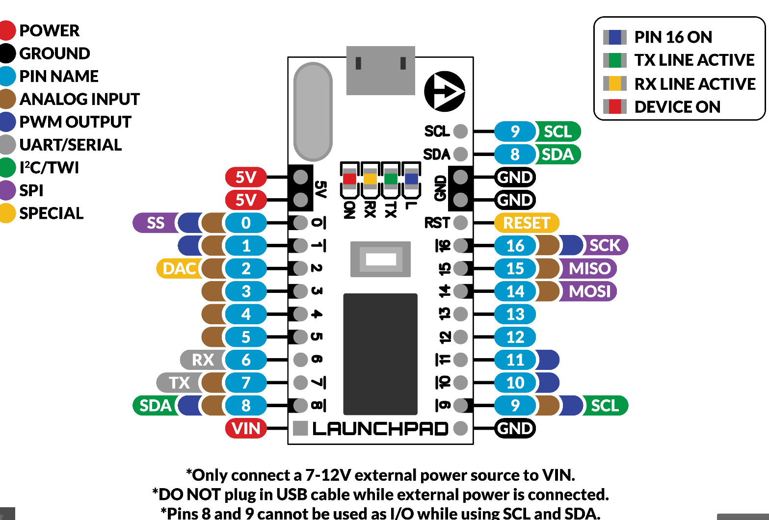
Launchpad Pinout
Specifications include for the Current Version (Version 1.0) includes:
Breadboard-friendly pinout
Micro USB type B connector
Microchip ATtiny1616
20MHz clock speed
16kB of flash memory
2kb of RAM
256 bytes of EEPROM
18 I/O pins (1 is currently configured as the reset pin)
8 PWM outputs (8-bit resolution)
12 analog inputs (10-bit resolution)
1 true analog output (0 – 4.3V)
UPDI programming interface
1 UART
1 SPI
1 I2C
Configurable custom logic (CCL) pins
tinyAVR 1-series architecture (similar to the megaAVR 0-series chips on the Arduino Nano Every and Uno WiFi rev2 boards)
OptibootX bootloader
CH340G USB to serial converter
AMS1117 5V LDO voltage regulator
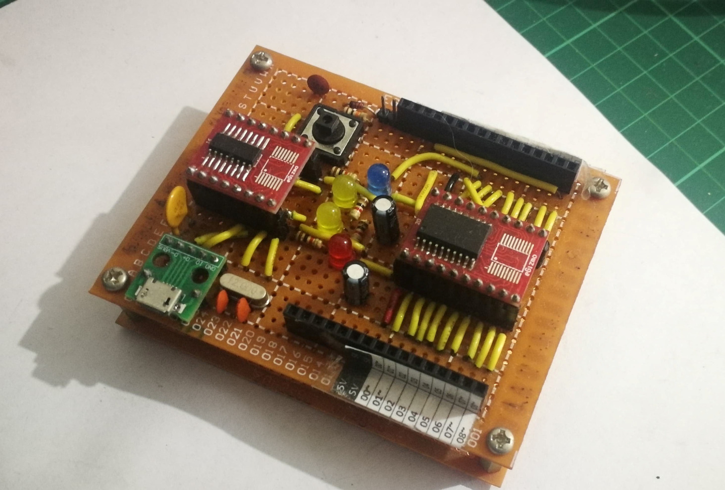
The Board’s Progress
About sales plan, Corpuz says :
“Well, probably. If there is demand I probably will. However, I surely will not be able to sell these at the $2 price mentioned since that only covers the cost of the components and does not include labor and assembly. I’m still assembling boards via hand-soldering so it will take a bit of time and effort to produce.”
Considering the fact that this project is probably the first time Corpuz has ever designed a PCB, we must commend him for his efforts. He says :
“I had to read up a lot on PCB design, concepts, and stuff regarding working with EDA’s. Considering this, I’m very proud of my work and I’m glad to share it all with you.”
The design is open source, and Corpuz will release the design files eventually once He is happy with a version he deevisms “releasable.” Regardless, he is still obliged to release the design files if He puts the board up for sale. For more information on about the board, visit Corpuz’s project page on Hackaday.
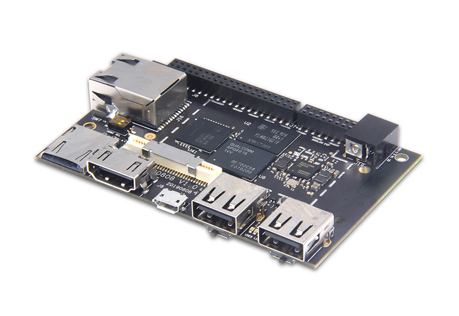
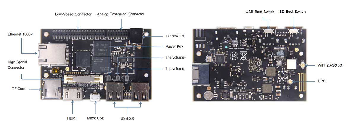
Developer Board 4 V3 is a single board computer based on Qualcomm Snapdragon 410E SoC with 2GB DDR3, 16GB EMMC, HDMI, MIPI-CSI, 40- and 60-pin expansion connectors. Fully structurally compatible with the 96boards CE standard.It features advanced processing power, WLAN, Gigabit Ethernet, Bluetooth, GPS, all packed into a board the size of a credit card.The DB4 V3 is designed for a variety of embedded and IoT categories. These include robotics, cameras, set-top-boxes, wearables, medical devices, vending machines, building automation, industrial control, digital signage etc.
Highlights
Compliant with the 96Boards Consumer Edition (CE)
Flexible expansion of mezzanine board
Custom 64-bit Kryo quad-core CPU up to 1.2GHz
Qualcomm® Adreno™ 306 GPU
1-2GB RAM, 8-16GB Flash
WLAN 802.11 n/ac Dual Band, Gigabit Ethernet and Bluetooth 4.1
Support Linux, Android and Windows 10 IoT core
Qualcomm Snapdragon 410E quad-core
Developer Board 4 features Qualcomm Snapdragon 410E processor, a Quad Core Qualcomm® Adreno™ 306 at up to 1.2GHz clock speed per core, capable of 32-bit and 64-bit operation.
2G + 16G
The utilization of eMMC memory offers an array of benefits in terms of performance security and reliability,resulting in a richer end-user experience
Connectivity: 802.11ac Gigabit Ethernet WiFi, Bluetooth
RJ45 10/1000M LAN provides more stable local network for video streaming.Dual band 802.11ac Gigabit Ethernet WiFi gives wider signal coverage and less interference.
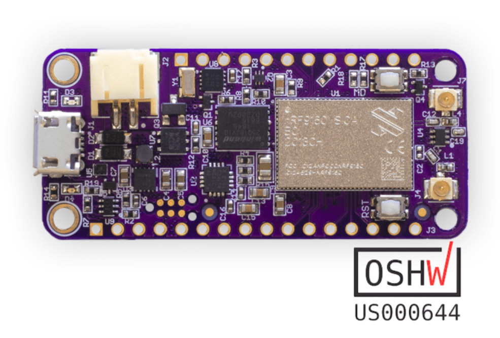
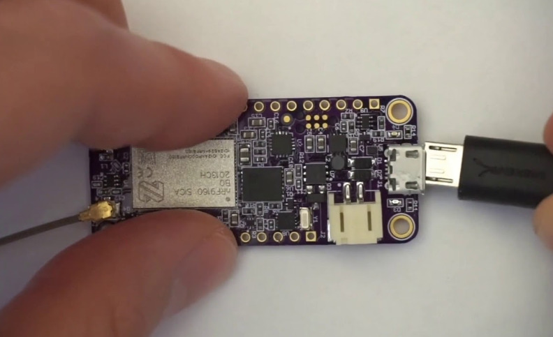
The nRF9160 Feather by Jared Wolff (aka Circuit Dojo LLC) is an electronics development board, which is a system-in-package part of nRF91 series that enables NB-IoT and eMTC (LTE-M) IoT connectivity, as well as assisted GPS. The package is available in an Adafruit Feather form factor. nRF9160 Feather board supports both CAT M1 LTE and NB-IoT for communication with the outside world, and can be powered by a USB power adapter or a LiPo battery and runs Zephyr OS via the nRF Connect SDK.
Specifications for the nRF9160 Feather include:
SiP – Nordic Semiconductor nRF9160-SICA LTE-M/NB-IoT/GPS SIP with Arm Cortex-M33 MCU, 1024 KB flash, 256 KB SRAM
Storage – Onboard 4MB NOR flash (note: upgraded from initial 2MB)
Cellular Connectivity – LTE Cat-M1 (eMTC) and LTE NB1/NB2 (NB-IoT) plus 4FF SIM card slot, and u.FL connector for an external antenna
GNSS – Built-in assisted GPS support plus u.FL connector for an external antenna
Expansion – Feather I/Os (12+16 through holes) with digital and analog I/Os, I2C, UART, SPI, RST, 3.3V, VBAT, GND
Debugging & Programmer
Serial console via micro USB Port connected to onboard USB to serial chip
Support for Jlink and CMSIS-DAP based programmers using a Tag Connect TC2030-CTX-NL over Serial Wire Debug (SWD)
Misc – “Uber” low-power RTC, reset button, user button
Power Supply
5V DC via Micro USB port
2-pin JST header + charger IC for LiPo battery (300 mAh or more required)
Power Consumption – 2µA of current in standby mode
Dimensions – 50.8 x 22.86 mm (Adafruit Feather form factor)
OSHW Certifications – US000664
About the board, Jared Wolff says
“The nRF9160 Feather is a true Feather, and then some, board. As you would expect, It works well across both USB and LiPoly batteries. The board is designed to be nice to your batteries. Not only can you take advantage of Nordic’s advanced power states, but you can also put the device into a low power standby state. Laboratory measurements are putting that mode at about 2µA of current. 2µA! The nRF9160 Feather is also designed to take harness every last mW your battery has to offer. That means from full-to-empty it’s using every last mW your battery has to offer. It runs at 3.3V and can support and work with most Featherwing boards!”
You don’t need an external programmer, you can just load your applications directly to the nRF9160 Feather. This helps save you from extra costs associated with getting started with your nRF9160 Feather. Also, the MCUBoot boot-loader and command-line tools have been tweaked to boost loading speeds by 10x. This makes loading via the boot-loader almost as fast as using an external programmer!
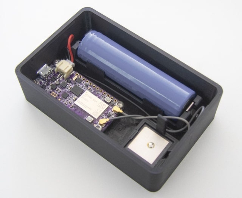
nRF9160 Feather enclosure
This campaign is courtesy Hackster Launch, which is a collaboration between Hackster.io and GroupGets. The board is certified by the Open Source Hardware Association. This means you can build yours with the available files. With the hardware licensed with CERN 1.2, mcuboot firmware with Apache 2.0, and documentation with CC-SA-4.0. nRF9160 Feather board goes for $99 with an LTE/NB-IoT Antenna and a Hologram Cellular IoT SIM card, with additional options which includes a $10 GPS antenna, and a $19 enclosure with GPS antenna and 18650 battery holder. Campaign scheduled end date is Wed, 19 Aug 2020 20:00:00 PDT. You can find more information on GroupGets’ campaign page.
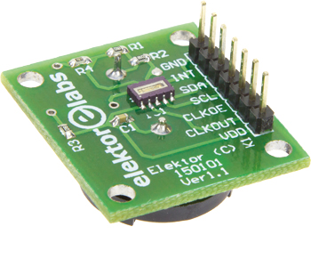
Off-air awfully accurate drop-in RTC & calendar on I²C
This RTC & Calendar board is built around Micro Crystal’s type RV-3029-C2 integrated circuit. The ‘3029 is a real-time-clock/calendar (RTC) cheerfully communicating via the I2C protocol. It offers good precision out of the box, and fine precision when tweaked.
Features:
Micro Crystal RV-3029-C2 RTC/Calendar chip
Battery backup
Selectable clock output
6 ppm max. error default
3 ppm error achievable with DTCXO tweaking
I2C connectivity
Free Arduino test & config utility
Drop-in module
Free Elektor Article: The RV-3029-C2 “Swiss Clock” – [Link]
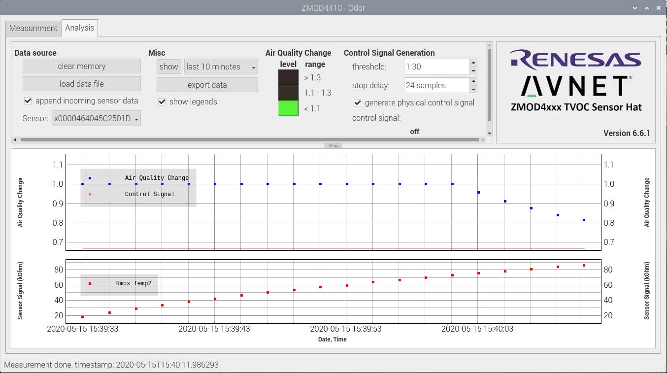
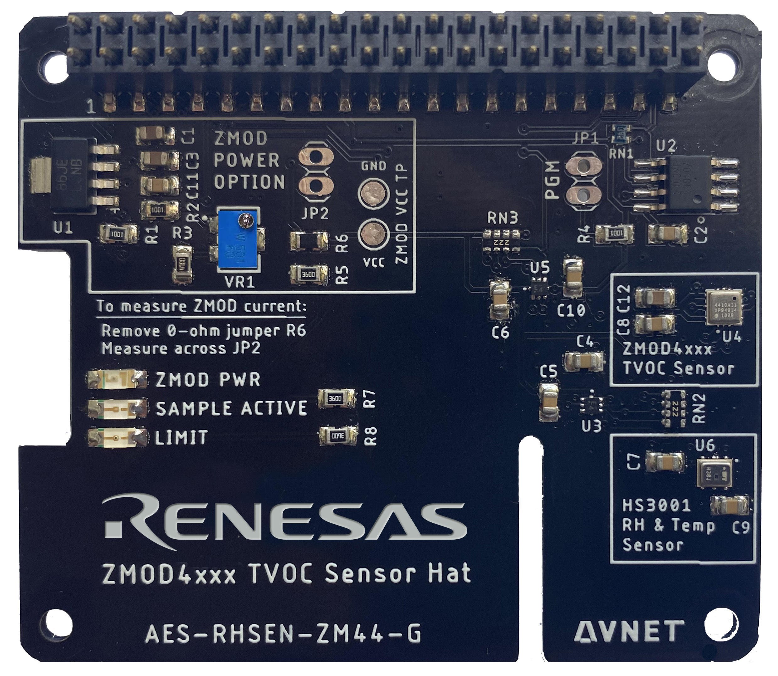
Sensor HAT based on Renesas ZMOD4410 module accelerates design of products requiring indoor air quality measurement capabilities
Avnet’s Renesas ZMOD4410 Indoor Air Quality HAT for Raspberry Pi is an evaluation, development and quick-prototyping tool intended for professionals developing a wide variety of mains-powered and battery-powered products with indoor air quality monitoring capability. The HAT features an on-board calibrated ZMOD4410 sensor that measures the concentrations of Total Volatile Organic Compounds (TVOC) and can estimate carbon dioxide (eCO2) levels. These are important indicators for monitoring indoor air quality. All sensors are electrically and chemically (gas) tested with calibration data stored in the ZMOD4410’s built-in nonvolatile memory.
In addition to the ZMOD4410 sensor, the HAT incorporates a Renesas HS3001 Precision Relative Humidity and Temperature Sensor, along with software-controlled status LEDs.
In certain applications, it may be desirable to shift the ZMOD4410 sensing element’s chemical selectivity and sensitivity, or to model its operation at supply voltages other than 3.3V. The HAT facilitates this with a user-adjustable power supply; a jumper selects the default fixed 3.3V supply or one which can be set from 1.75V to 3.9V. The HAT also provides connection points to measure the ZMOD4410 current consumption. This may be useful when integrating the sensor and its software into an extended-life battery-powered product.
Please note that algorithm libraries developed by Renesas are required to operate the ZMOD4410 sensor and convert its data into TVOC and eCO2 measurements. These algorithm libraries are not included with the HAT, but are available directly from Renesas subject to the terms and conditions of Renesas’ Software License Agreement. An application for the ZMOD4410 Software License Agreement, along with the procedure to download the algorithms and related confidential data, is available here.
To validate the HAT’s operation and begin measuring TVOC and eCO2 “out of the box” with a Raspberry Pi solution, Avnet provides a pre-compiled test application built with those algorithm libraries that runs under the Raspberry Pi operating system (formerly Raspbian).
Benefits:
Convenient Raspberry Pi HAT form factor for evaluation, development and quick prototyping of products that monitor indoor air quality
Detects a wide range of TVOC, from parts-per-billion to parts-per-million and provides eCO2 levels
Sensors are chemically tested and factory calibrated
On-board user-adjustable power supply option and current measurement connection points
Configurable alarm/interrupt output
Supplied with pre-compiled Raspberry Pi OS test / validation application
Renesas offers licensed downloadable compiled code, enabling a product road map of indoor air measurement innovation
Target applications:
Smart home appliances
Smart thermostats
Smart speakers
Smart fans
Smoke alarms
Vacuum cleaners
Garage openers
Security systems
HVAC controls
Air purifiers
Building automation
Software downloads:
Download the “out of the box” test/validation application for the HAT which is a pre-compiled application built with Renesas’ ZMOD4410 algorithm libraries and runs under the Raspberry Pi OS.
Download Renesas’ Software License Agreement and procedure to download the ZMOD algorithm libraries and related confidential data.
The concept of “a connected car” is no longer a figment of the imagination of movie producers but an everyday reality. Different communication protocols along with data from different sensors are being leveraged across the automotive industry to provide advanced features/services like usage-based insurance to users while monitoring different parameters that indicate the health of the car to ensure safety.
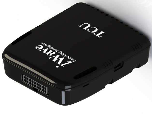
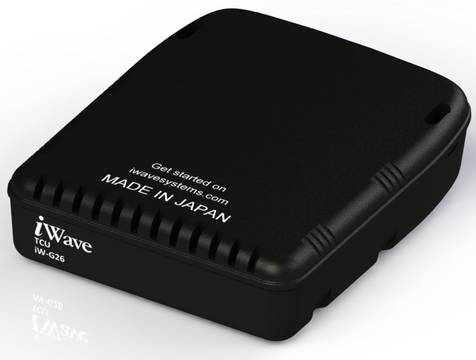
There are different approaches/levels to data collection, processing, and automation across the industry. While its factory fitted in-built for some cars, others support add-on systems that are currently regarded as the best route for flexibility. iWave Systems, the company behind the Linux based OBD-II Dongle has been at the forefront of developing telematics solutions for cars for a while, pushing the boundaries of standards across the industry. In line with this, they recently announced a new telematic controller unit.
The new TCU comes equipped with 4G, Wi-Fi and BLE communication features that help build a connected network within the vehicle while collecting exhaustive data from its electronic systems and the CAN network in a manner that enables real-time analytics.
Aimed at applications like fleet management, light-duty vehicle monitoring, user-based insurance, and many more, the new TCU features a 792MHz ARM Cortex A7 processors which provides an opportunity for real-time Edge Analytics based applications.
Some highlight features of the TCU include:
Certified with CE/FCC
Supports latest CAN FD, HS CAN, LS CAN, Ethernet CAN
Linux 4.1.15 based platform for generic applications
Secure FOTA support
J1962 compliant OBD II Protocol (ISO 15765-4 CAN)
High accuracy GNSS receiver with AGPS support
Battery for Anti-theft Alarm
Multi-cloud support
Designed to withstand the rugged nature of the in-car environment, the TCU has tolerance for extreme operating conditions and will perform fine in a temperature environment between -40°C to +85°C (Excluding Battery).
Some more technical specs for the device are provided below:
Arm® Cortex®-A7 based CPU @ 792MHz
DDR3L SDRAM – 256MB
eMMC Flash – 4GB
Connectivity
4G LTE
802.11 b/g/n Wi-Fi Module with Antenna with WPA2 feature
Bluetooth 5.0
Positioning
GPS Receiver with Antenna
Sensors
3 Axis Accelerometer
3 Axis Gyroscope
3 Axis Magnetometer*
OBD Features & Protocols
12V Power Input from TCU Port
USB 2.0 device
HS CAN x 1 Port support
LS CAN x 1 Port support*
CAN FD x 1 Port support*
GPIO’s x 4 (2 Digital IN, 2 Digital OUT)
Mic
Status LED (Configurable) x 1
Micro SIM/Nano SIM*/e-SIM*
ISO 15765-4 CAN protocol support in TCU Port
Temperature
-40°C to +85°C (Excluding Battery)
(i) The battery when discharging: -20°C to +60°C
(ii) The battery when charging: 0°C to 45°C
Form factor
106 X 87 X 28.5 mm (approximate)
For software, the device is capable of sending GPS, Accelerometer, and CAN data to the cloud over 4G through MQTT thus, the device is compatible with most device cloud platforms.
No price information is provided on the product page, but iWave typically sells within a B2B arrangement and you may need to reach out to them to get the actual price for the device.
New M5StickC PLUS, one of the core devices in the M5Stack series, is a mini IoT development board powered by ESP32-PICO-D4 with Bluetooth 4.0 and WiFi.
The M5StickC Plus development board was designed to take away a lot of stress off the development process. What can it do? The M5StickC Plus development board can help you to easily realize your ideas, enrich your creativity, and shorten the time for your IoT prototyping. It was built based on a growing hardware and software ecosystem with quite a number of compatible modules and units that help to maximize every step of the building process.
The new M5StickC Plus development board is an upgrade to the original M5StickC, with improvements like a bigger screen of about 18.7% increase (1.14″ 135 * 240 LCD display), a built-in passive buzzer, a battery capacity increase of 25mAh (from 95mAh to 120mAh), a more stable hardware design as well as support for HAT and unit family of products.
The M5StickC Plus development board has other rich hardware resources that are also present in the M5StickC like the PMU, IMU, microphone, RTC, LED, infrared, extendable socket, Grove port, wearable and mounted the wall, etc.
Key Features/components of the kit and Specifications include:
ESP32-based (with all of its features)
4 MByte flash memory
520KB RAM
1.14 inch colorful LCD display with 135 * 240 resolution
2.4G 3D antenna
Built-in Passive Buzzer
IR transmitter
6-axis motion processing unit (SH200Q)
SPM1423 Microphone
BM8563 RTC
AXP192 PMU
1x USB Type-C port
1x Grove port (12C, I/O, UART)
2x custom buttons
1x red LED
Wearable and mounted wall
Extendable Socket: G25 Output ExtPin
Built-in LiPo Battery with 120mAh capacity @3.7V
5V Power supply at 500mA
Temperature Range of 0°C – 40°C (32°F – 104°F)
Dimensions: 48.2 mm x 25.5 mm x 13.7 mm
Weight: 15 grams
The M5StickC Plus development board is a cost-efficient and an ultralow-power consumption board. It is applicable in creating light-weight wearable devices, IoT terminal controllers, and stem educational products and DIY projects.
More details on the M5StickC Plus dev board can be found on M5Stack’s product page where the tiny device is currently available for sale at $13.95.
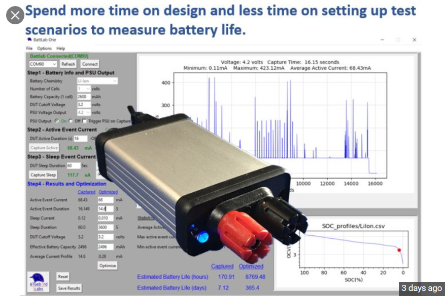
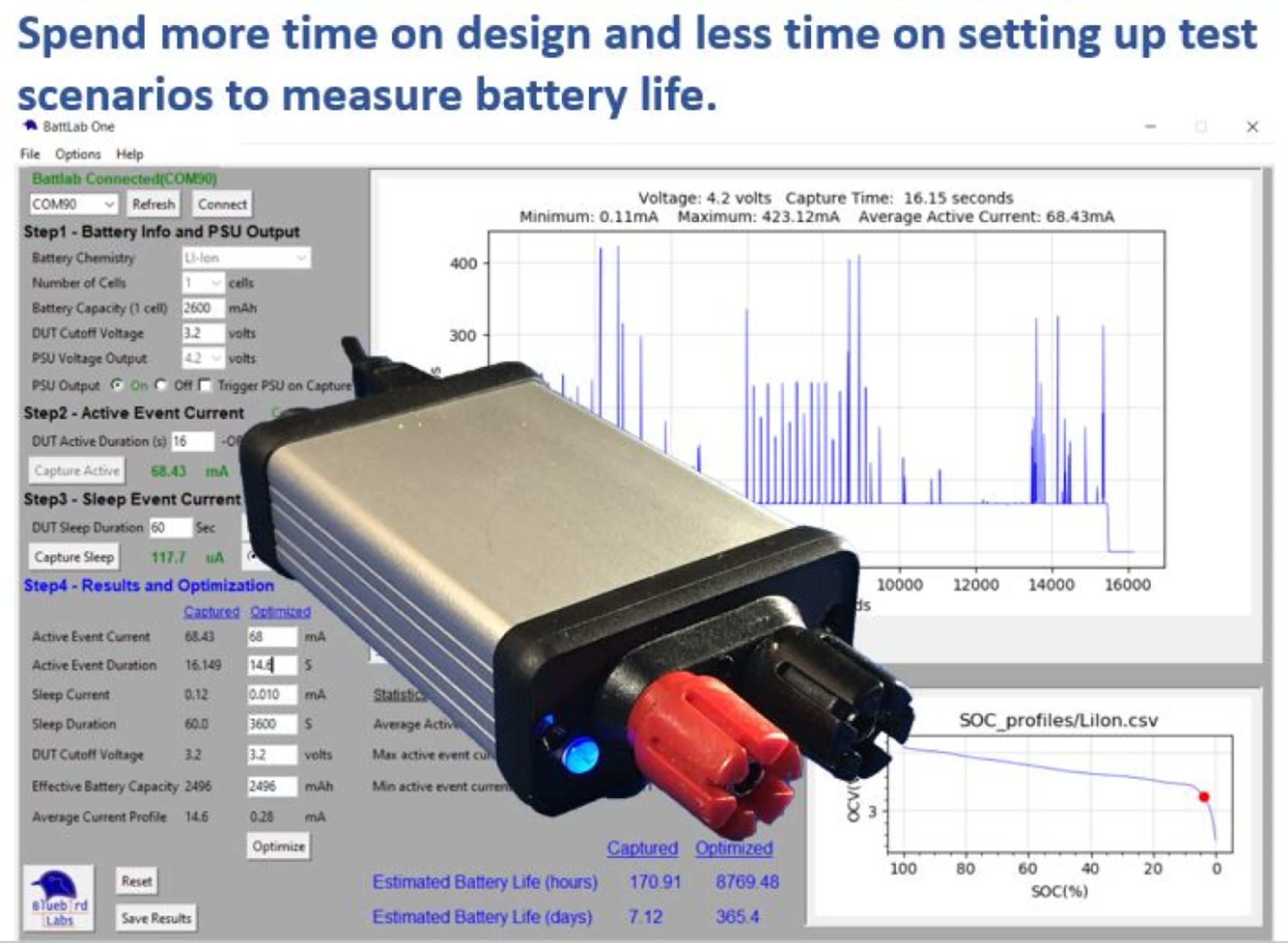
One of the problems developers in the world of IoT devices experience when building battery-powered devices over time is the process of measuring and estimating battery life, which can be very tedious. The process is tedious and cumbersome, with multiple test equipment arrangements to capture current profiles for different firmware states, manual data logging, and spreadsheets for data input and calculations to get to an estimate of battery life for the device under test (DUT). It is also quite hard measuring the amount of energy being consumed by these IoT devices due to the dynamic nature of the current consumption, with conventional measurement methods like multimeter, and oscilloscope having drawbacks. One method developers use is to use multiple instruments and hand calculations to arrive at an estimate of the energy consumption, but this method could be tasking. One device we have seen that solves this problem is the ZS1100A, which functions by plotting the current consumption vs time very accurately and in great detail, which can be used along with the battery model to estimate the overall battery life.
However, Doug Peters has built his own device called the BattLab-One (Battery Laboratory). It is a hardware/software solution that instantly captures insights of your design on battery life. His goal is to deliver a design tool that quickly and effortlessly provides an estimate of battery life and lets him optimize it for his projects, enabling him to spend more time on design and less time on measuring and calculating battery life.
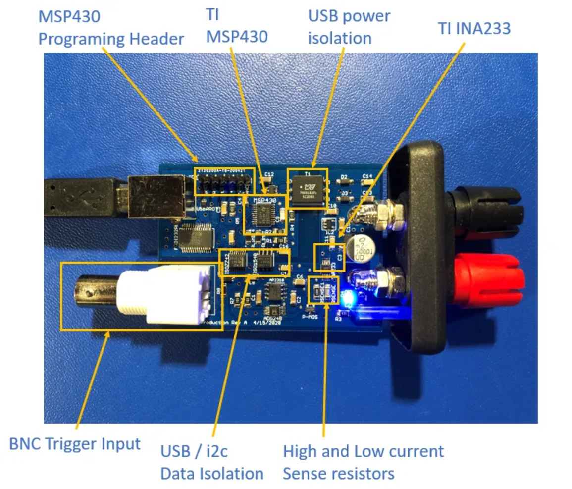
The BattLab-One Hardware
The BattLab-One Hardware functions by replacing the battery of the IoT project with a power supply unit, which enables standard battery voltage output simulation and then uses the built-in current sense technology of the BattLab-One to capture the current consumption profile of your device. By replacing the battery of any battery-powered project with a power supply unit that simulates your battery, the BattLab-One enables you to understand the impact of multiple parameters on your product’s battery life. It helps you to capture both active event and sleep mode current from 10uA to 500mA. It is compatible with MSP430 microcontroller-based device that simulates standard batteries for Li-Ion, LiFePO4, Alkaline, NiMh, NiCd.
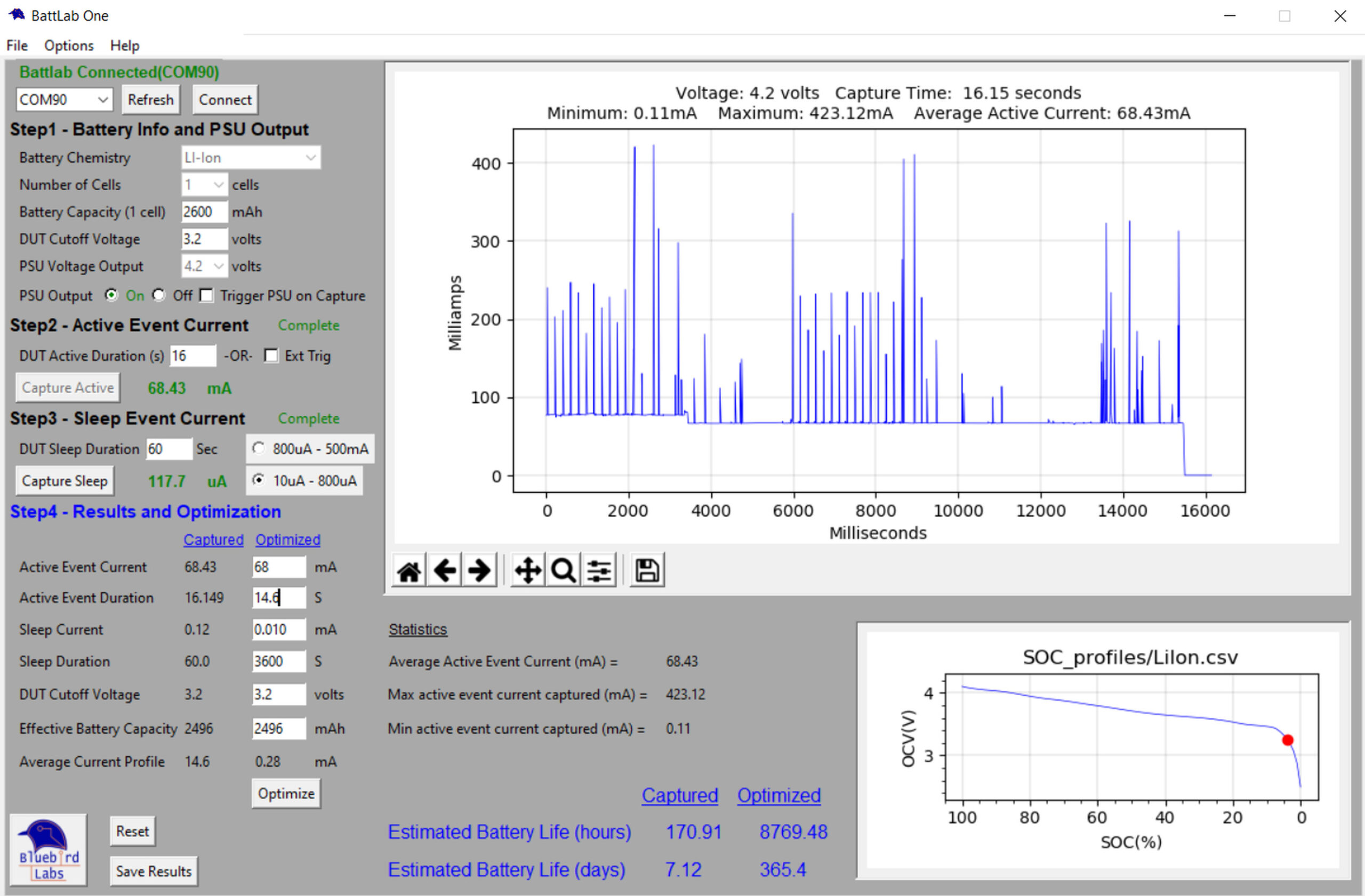
The BattLab-One Software
The device enables voltages of 1.2V, 1.5V, 2.4V, 3.0V, 3.2, 3.6V, 3.7V, 4.5V at up to 450 mA, and it is perfect for measuring your ESP8266 devices power demands. It has a 1kHz Sample rate, and 16 bit delta-sigma ADC. The device triggers input to capture firmware states and their impact on overall battery life and also offers what-if optimization analysis to improve the design of your project/product. The device also enables you to save profiles so you can compare your DUT current profiles, and offers interactive/detailed active current plot so you can look for anomalies and identify performance improvements for your product or project. To avoid ground loops, USB power, and data isolated from PSU output.
The device is open-source in hardware and software, and you can find documentation on Bluebird Labs website. You can purchase the BattLab-One on Tindie for $99 with enclosure, and for $79 with no enclosure.
This tutorial is an introduction to the Operational Amplifiers, also known as op-amps. The fundamental goal of op-amps is to amplify a voltage difference and it is the reason why we also describe them as differential amplifiers.
Op-amps have been invented the exact same year as the transistors (1947) and they were originally designed with vacuum tubes in order to perform basic mathematical operations. Mass-production only started in the ’50s when the op-amps were heavy, not reliable, and cost much. Not before the late ’60s were produced large amounts of transistor-based op-amps available for just a few $.
Nowadays, op-amps are one of the most used electronic components, their cost is only of a few cents of $, and thanks to their interesting properties they are used for many applications.
In the first section, we will present in detail the architecture and definitions surrounding op-amps. Moreover, we briefly discuss the internal circuitry of op-amps.
The second section focuses on the concept of the ideal op-amp which is a model describing the functioning of a perfect op-amp.
Real op-amps will be discussed in the third section where we will look into the differences that must be considered.
Presentation
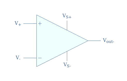
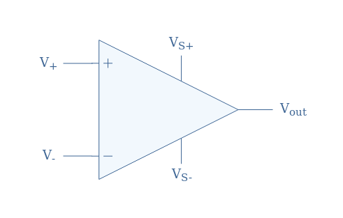
An op-amp is usually represented as a triangle with 5 pins from which 4 are inputs and one is the output.
fig 1: Representation and pin configuration of an op-amp
The output is labeled Vout and it is the pin where the output voltage is collected. V+ and V– are respectively the non-inverting and inverting inputs. VS+ and VS- are respectively the positive power supply and negative power supply rails.
We can note that in most of the op-amps representations, the power supply voltages and pins are not represented in order to simplify the drawing. Most of the time, the power configuration is just assumed or not relevant to perform calculations on a specific op-amp.
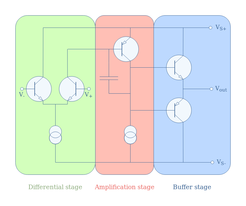
The internal circuitry of op-amps generally consists of a succession of bipolar or field-effect transistors and other passive components that are assembled in three distinct stages as shown in Figure 2:
fig 2: Simplified internal circuitry of an op-amp
The goal of the differential stage is to pre-amplify the differential signal V+-V– . The special configuration used to realize this process is called a transistor long-tailed pair circuit or differential pair. Moreover, this configuration provides a high input impedance.
The amplification stage is usually a high gain class A amplifier, the capacitor is used to assures the frequency compensation. Note that many amplification stages can be interconnected in order to provide a higher amplification output.
Finally, the buffer stage provides no amplification (unitary gain) but has a low output impedance and, therefore, provides high output currents. It is also used in order to adapt the impedances and protect against short-circuits.
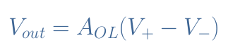
Open-loop gain
A few major characteristics can be associated with op-amps and we will dictate their electronic behavior here. The first one is the open-loop gain (AOL), it is a factor that represents the amplification applied to the input differential voltage:
eq 1: Definition of the open-loop gain
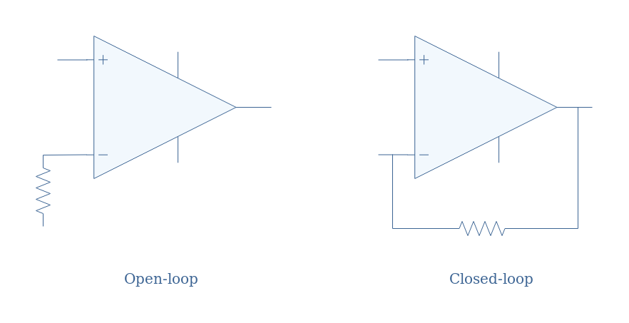
The term “open-loop” refers to the fact that no feedback is applied from the output to the inverting input of the op-amp. We will come back to that notion later on in the tutorial, however, in order to get an idea now of this concept, we show in Figure 3 the distinction made between open-loop and closed-loop op-amps:
fig 3: Representation of an open-loop and closed-loop configuration
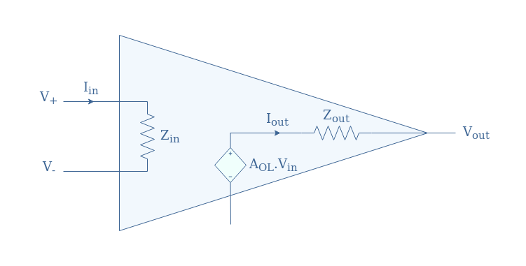
Input and output impedances
The input impedance Zin represents the ratio Vin/Iin with Vin=V+-V– and Iin being the input current. Similarly, we can also define an output impedance Zout which represents the ratio Vout/Iout with Vout=AOL.Vin and Iout being the output current.
Figure 4 below shows a representation of an op-amp that takes into account these impedances:
fig 4: Equivalent representation of an op-amp showing the open-loop gain, input, and output impedances
Bandwidth
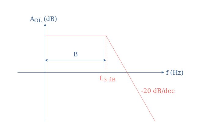
Op-amps can be used in DC but also in the AC regime, such as for example for the amplification of audio signals. For this reason, one of the important characteristics of op-amps is their bandwidth (B). This means that the gain (AOL) is dependent on the input frequency.
The bandwidth is measured in Hertz (Hz) and represents the range of frequencies that an op-amp can amplify efficiently. More precisely, the frequencies for which the gain is higher than -3 dB are included in the bandwidth. The limit frequencies for which the gain is exactly equal to -3 dB are called cutoff frequencies and often labeled f-3dB.
Op-amps behave actually as first-order low-pass filters, this means that the gain can be approximated as a constant from the DC regime up until its cutoff frequency. For higher frequencies, a loss of -20 dB/decade is observed as shown in Figure 5:
fig 5: Op-amp frequency diagram
To get more detail about this topic, we recommend reading the tutorial about Bode diagrams.
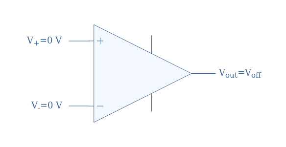
Offset voltage
The offset voltage Voff can be read at the output terminal when no input is applied to the amplifier. For example, if an op-amp has an offset voltage of 1 V, it means that the output voltage will constantly be shifted of +1 V, even when no input signal is applied.
fig 6: Illustration of the offset voltage
Ideal op-amp model
This model describes an idealized op-amp that is free of any parasitic phenomena. It is of course not possible to build such an op-amp with ideal characteristics but only approach it.
The ideal op-amp model consists of idealizing its main characteristics previously presented in the presentation section:
Infinite open-loop gain (AOL=+∞)
Infinite input impedance (Zin=+∞)
Zero output impedance (Zout=0)
Infinite bandwidth (B=+∞)
Zero offset voltage (Voff=0)
This set of idealized characteristics highlights the fact that an ideal op-amp does not disturb the amplified signal. An ideal op-amp is usually represented with a sign “∞” within the triangle shape.
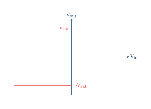
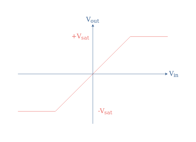
One very important property is that in an open-loop configuration, the output of an ideal op-amp can only take two values called the saturation voltages (Vsat). If the differential input Vin is positive (reciprocally negative), the output is +Vsat (reciprocally -Vsat).
fig 7: Vout=f(Vin) characteristic of an ideal op-amp in open-loop
The value of |Vsat| is slightly lower than the absolute value of the supply VS.
In the following subsections, we will see two different modes that can be adopted for an ideal op-amp depending on which input the feedback is applied.
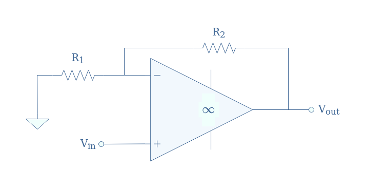
Saturated mode
In this mode, feedback is applied to the non-inverting input (+) of the op-amp. This means that any increase in the output voltage will increase the differential input. This kind of configuration is also known as a comparator and represented in Figure 8:
fig 8: Ideal op-amp in saturated mode (positive feedback)
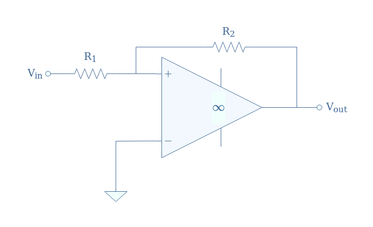
Linear mode
If instead the feedback is applied to the inverting input (-) of the op-amp, the function of the amplifier is completely different.
fig 9: Ideal op-amp in linear mode (negative feedback)
In this configuration, any increase of the output voltage tends to decrease the differential input and therefore, also tends to maintain a differential input close to zero.
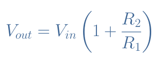
The relation between the input and output voltages is given by Equation 2:
eq 2: Transfer function of the op-amp presented in Figure 7
In a closed-loop configuration with negative feedback, the characteristic Vout=f(Vin) is therefore linear according to Equation 2 up until -Vsat and +Vsat where a plateau emerges.
fig 10: Vout=f(Vin) characteristic of an ideal op-amp in closed-loop
Real op-amps
Op-amps that can be found in real electronic circuits have limited and non-ideal characteristics:
Finite open-loop gain typically ranges from 105 to 106
Finite input impedance: 105 up to 1012 Ω
Non-zero output impedance: 50 to 200 Ω
Finite bandwidth
Non-zero offset voltage: 1μV up to 50 mV
The gain of real op-amps depends moreover on the frequency with a variation that can be described as a first order low-pass frequency. Another important information is that the product gain-bandwidth of op-amps is constant, this implies that “slow” op-amps can have higher gains and “fast” op-amps tend to have a lower gain.
The input impedance is not purely resistive as a parallel capacitor of a few pF modelizes the low-pass filter behavior of the op-amp and tends to reduce the impedance when the frequency increases.
Conclusion
We have presented the basics of operational amplifiers in this introductory tutorial. Op-amps are integrated circuits that are powered with two supply inputs and which goal is to amplify the differential input voltage.
We have briefly presented their internal circuitry and shown that at least three stages are necessary to perform amplification.
Many characteristics can define an op-amp, however, five in particular are extremely important and are presented in detail in the first section. Moreover, we explain that two configurations can be adopted leading to different behaviors: the open-loop or closed-loop.
The ideal op-amp model is detailed in a second section where its idealized characteristics and behavior are summarized.
Finally, we highlight the differences between this ideal model and real op-amps that can be found in many modern circuitry. The most important consequences of these differences are the finite gain and bandwidth which limits the amplification and frequency abilities.