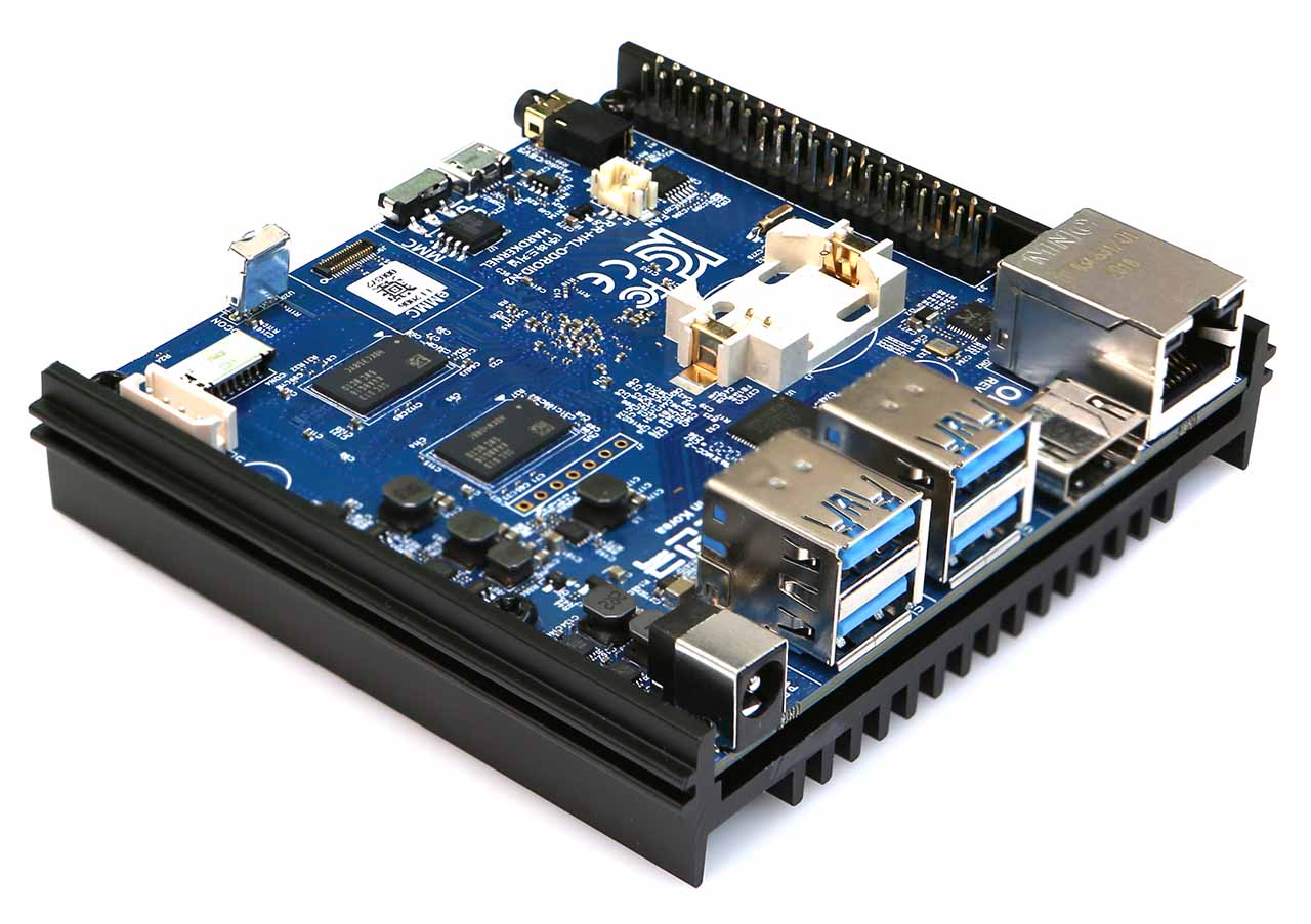
With Amlogic S922X Rev. C Processor Clocked at up to 2.4 GHz, Odroid-N2 Plus is possibly the fastest open-spec single board computer the world has ever seen.
The rising technological advancements in IoT plus the increase in demand for smart connected devices have resulted in more significant growth of the single board computer market over the past few years.
Barely 15 months after Hardkernel released ODROID-N2, one of the fastest ARM single board computer with hexa-core Cortex A7/A53 processor and 2GB/4GB RAM, the company has come back to announce an upgrade of the high-end SBC with what is likely to be the fastest open-spec ARM board around, the Odroid-N2-Plus or simply N2+.
The Linux-driven Odroid-N2 Plus takes advantage of a newly revised version of Amlogic’s S922X with advanced CPU core power rail and higher clock frequencies. The new Rev-C in the N2+ offers a 400 MHz clock speed boost over the Rev-A in Odroid-N2, bringing the 4x Cortex-A73 cores to 2.2 GHz from 1.8 GHz and the 2x Cortex-A53 upwards to 2.0 GHz from 1.9 GHz. With this speed, the N2+ board will probably match the more expensive SBCs on all sides.
Some highlight features and specification of the board include:
HDMI 2.0 up to 4K @ 75 Hz and composite video + stereo audio
2x LEDs, IR receiver and 2-pin header each for RTC battery and fan
Standard CR2032 coin cell battery holder for the RTC, and
7.5 – 20V DC input.
Operating Systems: Android 9 Pie, Ubuntu 18.04/20.04 and Linux 4.9.162 LTS
Weight: 200g
Dimensions: 90 x 90 mm (with heatsink) or 100 x 91 x 18.75 mm (without heatsink)
Hardkernel claims that the N2+ is capable of offering twice the performance of a Raspberry Pi after testing over 300 samples of the N2+ board to discover that 4x Arm Cortex A73 cores can also be overclocked to 2.4 GHz, about 33% performance increase over the original Odroid-N2 board and roughly twice the speed of a Raspberry Pi 4.
The 2GB version of the N2+ board is available for preorder on Hardkernel’s store for $63 while the 4GB version goes for USD $79, with shipping scheduled for July 20 and 24 respectively for both options. In addition to the mainboard, an optional $4 cooling fan is also available for users who may be running the board in an overclocked state or at high temperatures.
More details on the Odroid-N2 Plus may be found on the product’s announcemet.
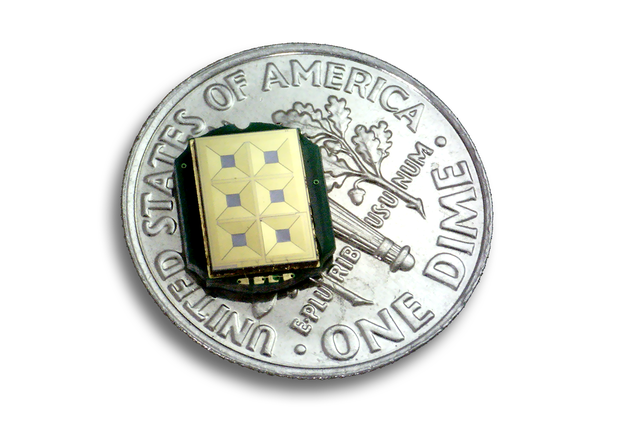
Today xMEMS Labs emerged from stealth mode to reinvent sound with the introduction of Montara, the world’s first monolithic true MEMS speaker, delivering high fidelity, full-bandwidth sound and low total harmonic distortion (THD) for sealed in-ear personal audio devices, including true wireless stereo (TWS) earbuds. Montara is also the world’s first IP-57 rated microspeaker, enabling water and dust-resistant earbuds. Consumers will benefit from enhanced audio fidelity with raised levels of clarity and detail for instruments and vocals, extremely low latency, waterproof earbuds, and longer listening times.
“With on-the-go media consumption on the rise such as subscription music, podcasts, video, audiobooks and mobile gaming, consumers are increasingly demanding enhanced audio quality and extended listen times between charges,” said Joseph Jiang co-founder and CEO. “Until now, the industry has relied on antiquated, centuries-old multi-component voice coil speakers requiring labor-intensive, high variability factory assembly lines. Our revolutionary Montara product is a game changer for delivering a new combination of audio fidelity, size, energy consumption and uniformity not possible with traditional voice coil approaches.”
Montara eclipses early hybrid-MEMS speakers by implementing the entire speaker (actuator and diaphragm/membrane) in silicon, reducing package height and eliminating driver matching and calibration due to inherent variability in membrane assembly. The combination of Montara’s design innovation and monolithic capacitive piezo-MEMS manufacturing material results in precise actuation, quality sound, speaker-to-speaker uniformity and repeatability.
“It’s exciting to see the first monolithically integrated MEMS (transducer and membrane), full-bandwidth microspeaker for the rapidly growing hearables market,” said Dimitrios Damianos, Technology & Market Analyst at Yole Développement (Yole). “The replacement of traditional voice coil speakers and balanced armatures with a complete semiconductor component provides a scalable design that claims significantly lower power and latency, while xMEMS’ fabless model ensures high volume repeatability. Technology advancements like these could improve the quality and adoption of in-ear personal audio devices.”
“I have reviewed the audio test data from xMEMS and from this it appears to be a viable product, maybe even a game changer for TWS and IEM earphones. One small step for audio, one giant step for MEMs speakers,” said Michael Klasco, president of Menlo Scientific.
Montara Features:
Sound Quality
Full bandwidth (20Hz-20kHz) with flat frequency response at >110dB SPL
Ability to replace multiple balance armature drivers with a single chip
Better SPL/mm3
Consistency
Highly uniform and reliable semiconductor process
Eliminates driver matching and calibration
Consistent silicon membrane movement enables active compensation for low THD (< 0.5% (200Hz ~ 20KHz))
Low Latency
<0.1ms mechanical latency enables active noise cancelation (ANC) across wider frequency range
Montara’s capacitive vs. current-driven architecture reduces driver power consumption
Water-proof: IP57 water immersion and dust resistance without special membrane
Small size with very low profile at 1mm thickness
Availability
Montara samples and evaluation kits are available in July to select customers, with mass production orders expected in the first quarter of 2021.Montara will offer two LGA package options: Standard (6.05 x 8.4 x 0.985mm) and Side-Firing (Phi 6.1mm; 6.05 x 1.0 x 8.4mm).
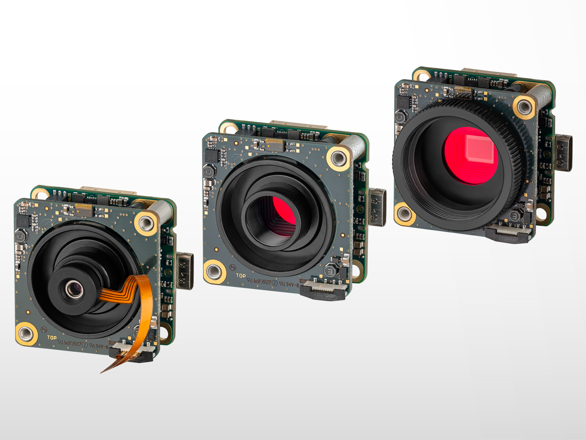
IDS extends selection of automatically focusable board-level cameras. Thanks to their practical autofocus function, uEye LE AF industrial cameras deliver perfectly focused images even with frequently changing object distances.
IDS Imaging Development Systems GmbH now offers additional camera variants with 2.1 and 3.1 MP Sony sensors which provide more flexibility in terms of application design and camera integration. For the first time, the company also offers models with upright USB Type-C alignment in this product family.
In addition to the previously available uEye LE AF cameras with 6.4 MP (IMX178, 58 fps) and 18.1 MP (AR1820HS, 20 fps) sensors, customers can now also purchase models with 2.1 (IMX290, 120 fps) or 3.1 MP (IMX265, 80 fps). All cameras feature a USB 3.1 Gen 1 interface, USB Power Delivery – which can be used, for example, to power an LED light source or a photoelectric sensor – and allow the use and control of liquid lenses.
The autofocus function ensures sharp images in the blink of an eye, even if the lens is not physically accessible or if the distance between the lens and the object changes frequently. The board-level cameras are therefore particularly well-suited for applications in fields such as logistics (e.g. for parcel acceptance and sorting) or traffic monitoring. Due to their compact design with dimensions of only 36 x 36 x 20 mm they also prove their strengths in embedded vision systems. This means that they are also interesting for integration into small medical or industrial devices.
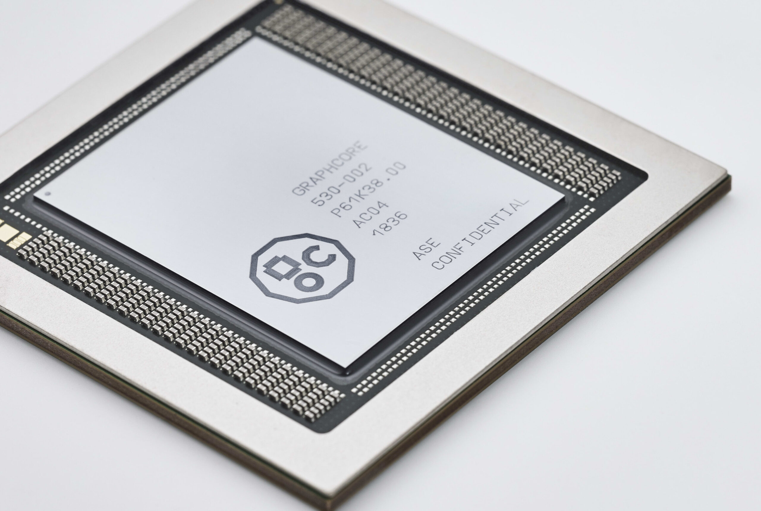
AI processor company Graphcore Ltd. (Bristol, England) has announced its second-generation ‘Colossus’ intelligent processor unit (IPU), the GC200, claiming the 7nm chip is the world’s most sophisticated microprocessor. By Peter Clarke @ eenewseurope.com
The company has also introduced a 1U board containing four GC200 processors that it calls the IPU-Machine or M2000.
The chip is manufactured by foundry TSMC in a 7nm FinFET manufacturing process allowing far greater integration than was possible with Graphcore’s first IPU, which was implemented in TSMC’s 16nm FinFET process.
Graphcore CEO Nigel Toon described the GC200 as “the world’s most advanced processor” in a Youtube video stating it contains 59.4 billion transistors, 1,472 independent processor cores able to support 8,832 computing threads in parallel. The chip has also tripled the amount of on-chip memory able to support processors moving up to 900Mbytes.
This results in a naked maximum performance of 250 TeraFlops of AI compute at FP16.16 and FP16.SR (stochastic rounding). The GC200 supports much more FP32 compute than any other processor, the company has claimed.
As with the first IPU the GC200 was designed to use Graphcore’s Poplar software development and management environment. However, the company has also introduced changes in data storage to increase off-chip memory bandwidth to 180Tbytes per second and in inter-IPU communications fabric, Toon said.
The net result is an 8x improvement in benchmarked performance compared to the first IPU. The company claims that systems based around its M2000 racks will be 16 times higher performance than similar ones based on 7nm GPUs from Nvidia.
The IPU-M2000 delivers 1PetaFlop of AI compute and up to 450Gbytes of memory. The newly developed IPU-Fabric enables the building of IPU pods for data centres connecting up to 64,000 IPUs. The M2000 is priced at $32,450.
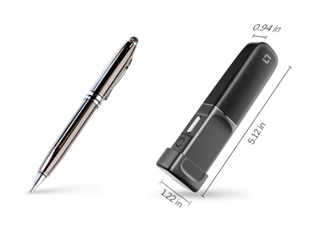
As we have featured earlier this month the Selpic P1 is going to launch on Indiegogo in late July. But what is Selpic P1? Is it another handheld printer going around or it has something more to offer?
Selpic claims this to be the world’s smallest Handheld Portable printer that enables you to print on almost any surface like using an ordinary pen. It’s highlights include:
Lightweight and Portable
Print Anything, Anywhere
600dpi print resolution
90 pages of ink capacity (5% in coverage)
up to 6 colors to choose from
3 hrs working time per charge
With its pen styled shape, you can carry it around with you and get ready to use it anytime. It can easily print text, images, graphics,QR codes, and barcodes even on porous surfaces. The print head features 300 tiny nozzles with 0.002 of nozzle spacing and each nozzle can eject 18m drops per second. This leads to a high-quality and clear print result in printing logos or anything else on almost any surface.
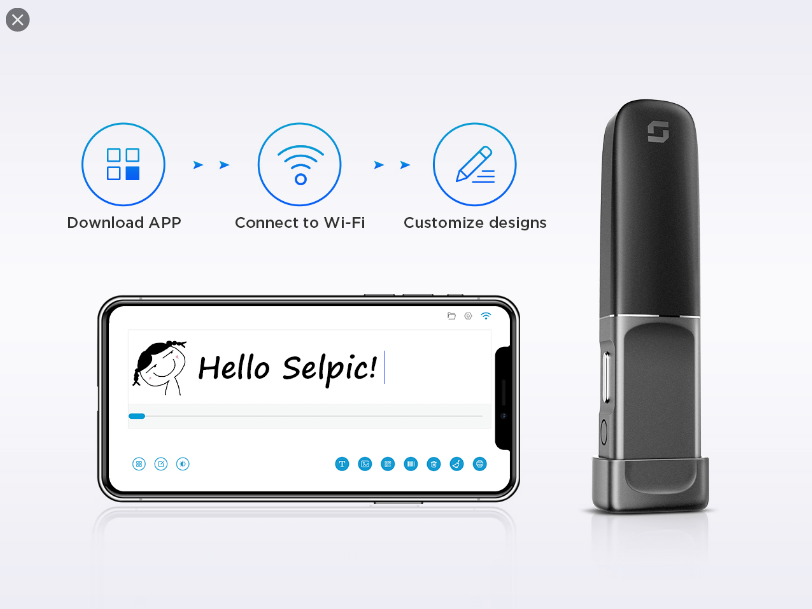
The printer comes along with a user-friendly smartphone APP that lets you define the print artwork. All you have to do is to connect the Selpic P1 with your smartphone over wifi and then you are ready to edit the artwork and print.
Hands-on Review
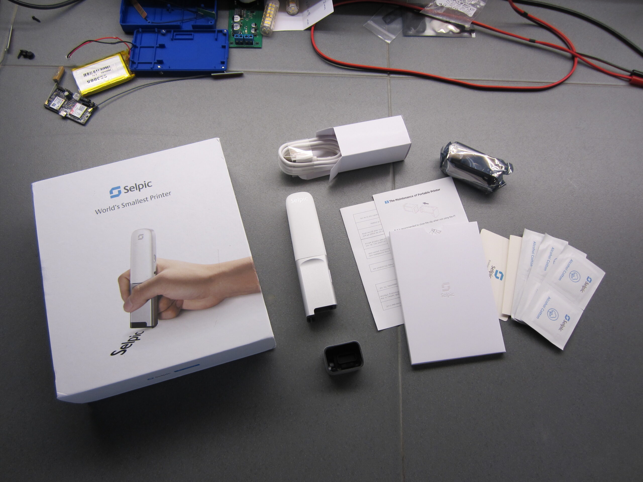
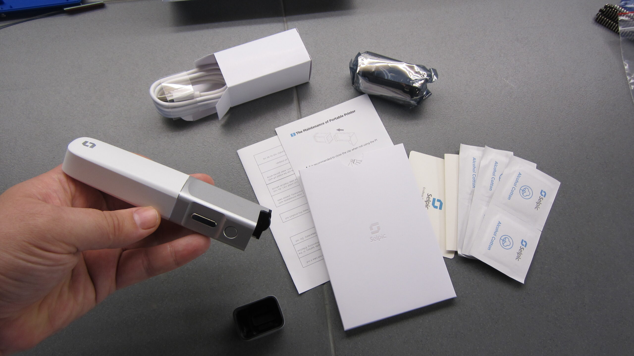
The printer comes in a good quality box that includes:
The handheld printer
1x ink cartridge
USB type C cable
Maintenance Manual
Alcohol wipes to clean the head
Guarantee Card etc.
Unboxing Video
Testing and Printing
To make your first print, you have to initially download the Android or iOS app from the appropriate app store. Launch the app to your smartphone and register for an account on Selpic if you haven’t already done it. The next step is to connect the Selpic P1 to your smartphone following the screen instructions. Once the connection is done, you will see the signal icon become light blue. Now you are ready to edit the text and icons using the inbuilt editor. We found the editor a little hard to use, because of the small icons and the not so self-explaining first three icons on the left side of the screen. You will need some time to familiarize your self with the app and when your artwork is ready you can click the far most right Print icon. The artwork is then transferred to the printer and you are ready to print. Grab the printer, hit the main button, and scroll it on the desired surface. Printing is started automatically as long as you scroll. Check the video above to see how this works.
Campaign
A campaign for the Selpic P1 is launcedh on INDIEGOGO with the device starting at only $99. There are several other packages planned with associated discounts. You can sign up to get notified for updates and also to get first option access to the diverse discounts like the super early bird discount of 55% off the $199 MSRP package which will be available to the first 500 backers.
While full-time embedded firmware developers like me may always have one thing or the other against the Arduino IDE, the truth is, the IDE remains one of the most versatile and widely used embedded development platforms in the world today. The success of the Arduino boards and related microcontrollers like the Atmega328p can be attributed to the versatility and ease of programming it brings, and one can easily link the success of more than 70% of microcontrollers/dev boards that have attained a level of popularity similar to the Arduino, to their compatibility with the Arduino IDE.
To benefit from the ease of programming offered by the Arduino IDE, communities around different microcontrollers build compatibility tools and one of the latest is the Sduino tool developed by Michael Mayor to facilitate programming of STM8 microcontrollers using the Arduino IDE.
The STM8 family of microcontrollers comprises the STM8S, STM8L, and STM8AF series of microcontrollers which are implemented around a high-performance 8-bit core and come with a state-of-the-art set of peripherals. They are manufactured using ST-proprietary 130 nm embedded non-volatile memory technology and support fast and safe development through enhanced stack pointer operations, advanced addressing modes, and new instructions.
The Sduino tool allows these microcontrollers to be programmed using the Arduino-C while and also supports the Standard Peripheral Library (SPL) which means the same code written on the Arduino IDE can be compiled with little or no modification on the official ST Visual Develop IDE.
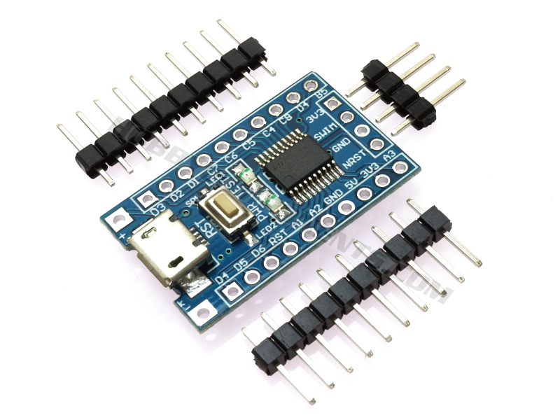
STM8S103F3 Development Board
Sduino is still under development and does not currently support a good number of popular Arduino libraries, but it supports enough to be useful. So for today’s tutorial, I will examine the process involved in setting up your Arduino IDE to program an STM8 based microcontroller. For demonstration purposes, we will use the STM8S103F Development Board, and our goal will be to upload the blink example to the board.
Ready? let’s go
Required Components
The following components are required to follow this tutorial:
The STM8S103F Development Board
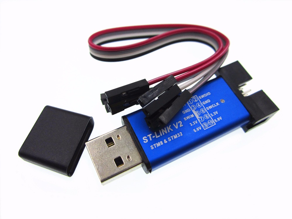
The ST link V2 programmer
A breadboard
Jumper wires
All of these components can be bought from your favorite electronics component store. We will use the LED onboard the STM8S103F development board, but if you will like to use a normal LED, you can add a LED and a 220 ohms current limiting resistor to the list of components.
Schematics
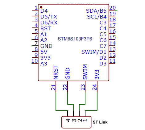
Since we will implement the blink example using the LED onboard the STM8S103F, there is not much to do in terms of schematics. However, for those who may not be familiar with the process of connecting the ST link programmer to the STM8S103F board, the connection is described in the schematics below:
Schematics
For clarity, a pin map showing how the components are connected is provided below;
Go over the connections again to ensure everything is as it should be. If you are using the ST-Link for the first time, you will be required to install the driver and set things up. In most situations, driver installations will start automatically immediately you connect the ST-Link programmer to your computer.
ST-Link v2
Arduino IDE Setup
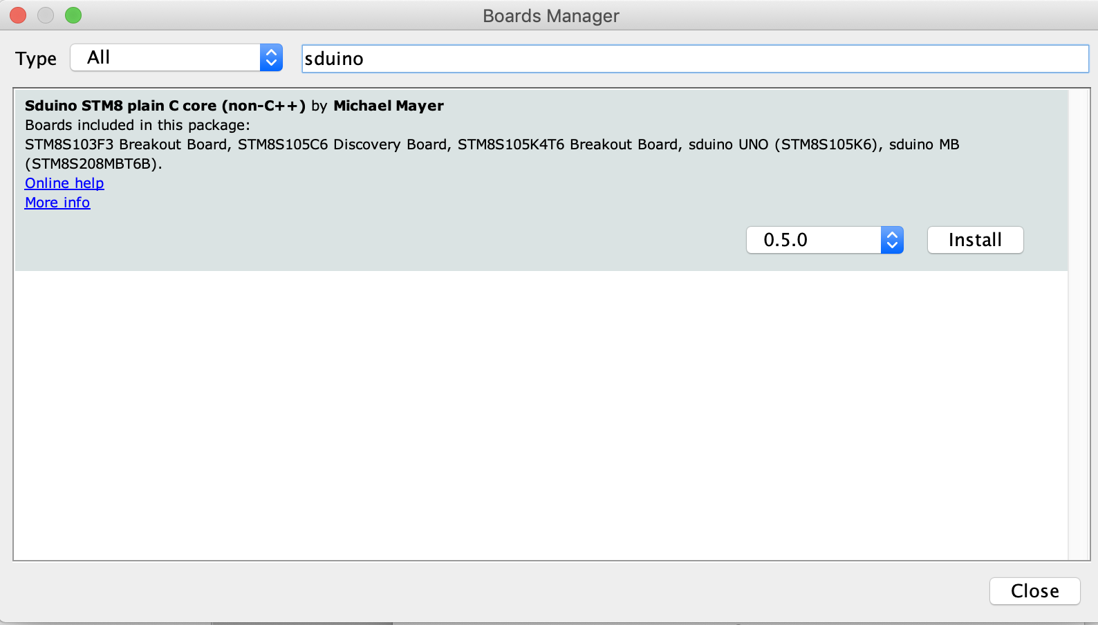
To make the process of integrating open-source boards with the Arduino IDE easier, the IDE comes with a feature called “board manager“. Through the board manager, new boards (essentially software-based components required for the Arduino IDE to be able to upload code to a particular MCU) can be added to the IDE. These software-based components, often called cores, are usually developed by manufacturers of the board (like Sparkfun does for its boards) or a group of users with the desire to see their board work with the Arduino IDE. The Sduino represents the core for the STM8s boards and we will be installing it on the Arduino IDE using the board manager. Follow the steps below to do this:
1. Open the preferences window from the Arduino IDE. Go to File > Preferences
2. On the preferences window, locate the “Additional Board Manager URLs” text box and enter this link; https://github.com/tenbaht/sduino/raw/master/package_sduino_stm8_index.json into the field as shown below. As you may have other URLs there already, separate the URLs from each other using a comma (“,”) and click OK when done.
3. Next, open the Arduino board manager. Go to tools>Boards>Boards manager
4. When the board manager opens up, enter Sduino into the search bar. You should see the Sduino core come up as shown in the image below. Click on the install button to install the core.
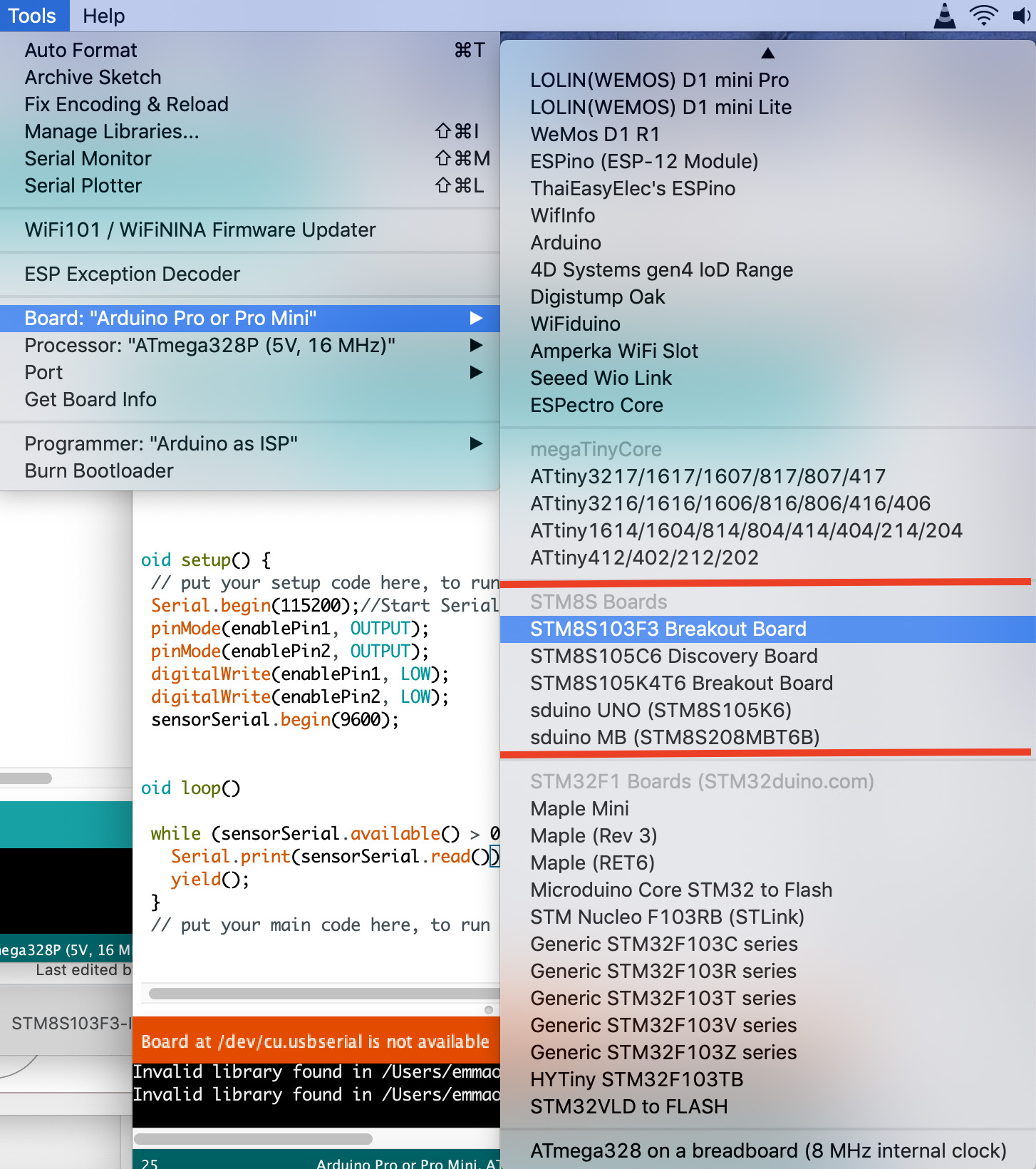
5. With the installation complete, close the board manager. The STM8s boards should now be available under the list of boards as shown in the image below.
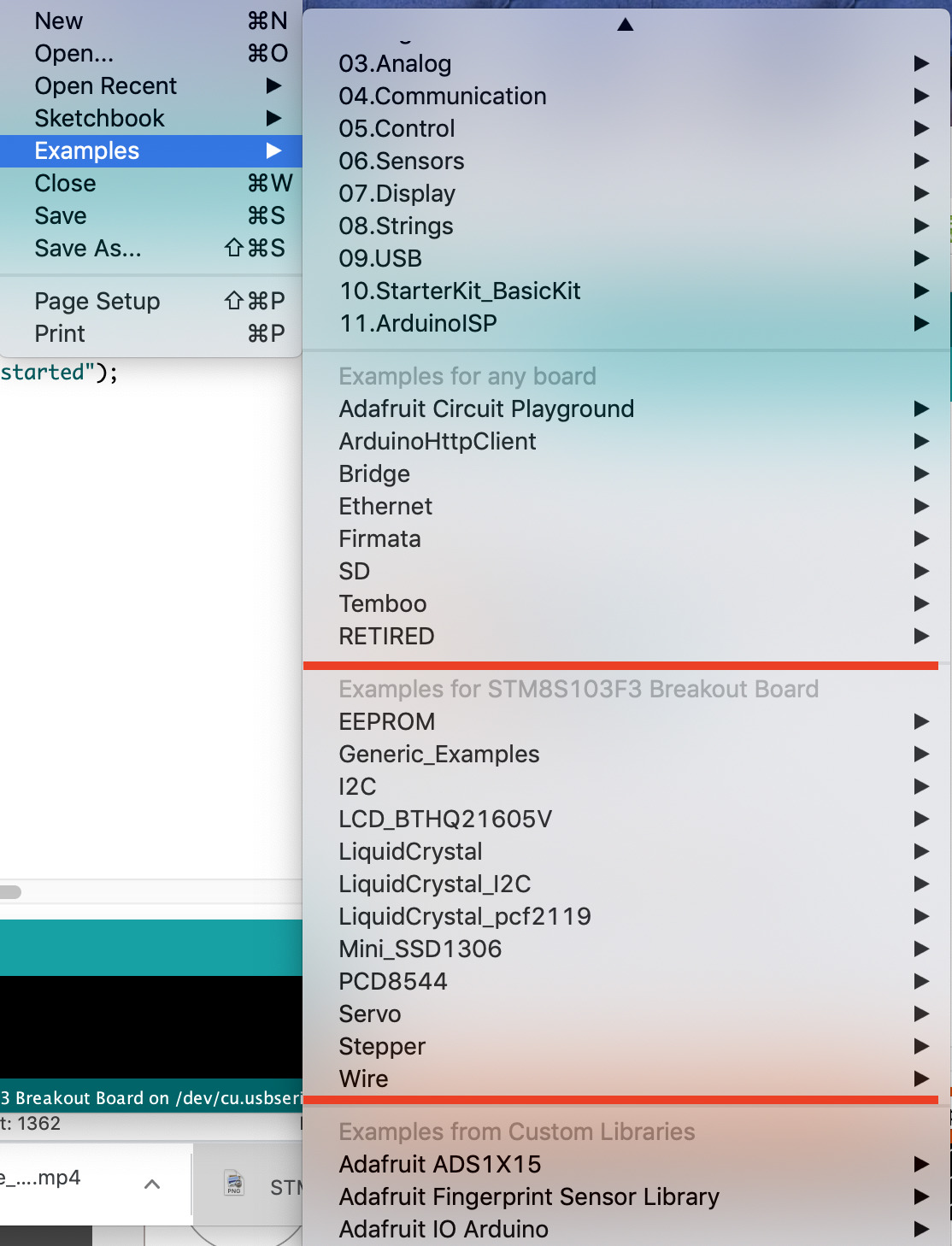
6. Installing the Sduino core will automatically install some Arduino libraries that have been modified to work with STM8s boards. Set your board type (by going to tools -> boards) to one of the STM8s boards, and go to examples (File -> examples). You will see a list of examples for the newly installed libraries.
With this done, you now have all you need to upload code to the STM8s boards.
Code
As mentioned during the introduction, for demonstration purposes, we will upload the blink example to the STM8S103F Development Board. You can use the generic blink example (File -> Example -> Basics -> Blink) or use the blink example among the STM8s Specific libraries (File -> Example -> Generic_Example -> Basics -> Blink).
I believe the code for the blink example needs no explanation and if you compare the two sketches you will see that they are exactly the same.
void setup() {
  // initialize digital pin LED_BUILTIN as an output.
  pinMode(LED_BUILTIN, OUTPUT);
}
// the loop function runs over and over again forever
void loop() {
  digitalWrite(LED_BUILTIN, HIGH);   // turn the LED on (HIGH is the voltage level)
  delay(1000);                       // wait for a second
  digitalWrite(LED_BUILTIN, LOW);    // turn the LED off by making the voltage LOW
  delay(1000);                       // wait for a second
}
Code Upload
Ensure your board is connected to the computer via the ST-link as described in the schematics. On the Arduino IDE, ensure the right board type is selected, and for set the programmer to ST-Link/V2 as shown in the image below:
With this done, hit the upload button, you should see the onboard LED begin to blink.
That’s it!
The Arduino IDE and Sduino provides a pathway to help you jumpstart development with STM8S. However, the platform is still under development and many Arduino libraries are yet to be supported.
That’s it for this tutorial! feel free to reach out to me via the comment section with questions or any clarifications you require.
Johanson Technology’s single antenna matching solution covers all relative frequency bands
Multiple frequency, protocol, and functionality solutions for IoT connectivity continue to push size and performance limits. To address this, Johanson Technology developed a multiband flexible solution using one antenna. This solution covers cellular (LTE), sub-GHz (868/915 MHz), GPS and/or GNSS (GLONASS), 2.4 GHz (Bluetooth® and/or Wi-Fi®) using one SMT chip antenna and two 6-channel RF switches. The entire solution requires a PCB area of about 360 mm, making it very compact with industry-accepted radiated gain and efficiency in a 51 mm x 51 mm board..
Features
Single antenna matching solution to cover all relative frequency bands
Can resonate at multiple frequencies
Requires antenna matching networks to cover cellular/sub-GHz/GPS-GNSS/2.4 GHz bands to achieve high efficiency and bandwidth
Entire solution requires a PCB area of about 360 mm, making it very compact with industry-accepted radiated gain and efficiency in 51 mm x 51 mm board
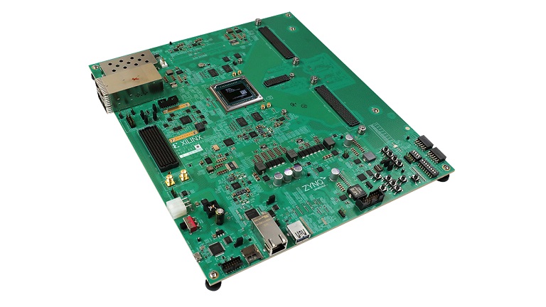
The Zynq® UltraScale+™ RFSoC ZCU208 Evaluation Kit is the ideal RF test platform for both out-of-box evaluation and cutting-edge application development.
The Xilinx Zynq UltraScale+ RFSoC ZCU208 ES1 Evaluation Kit features a Zynq UltraScale+ RFSoC ZU48DR, which integrates eight 14-bit 5GSPS ADCs, eight 14-bit 10GSPS DACs, and eight soft-decision forward error correction (SD-FEC) cores designed to jumpstart RF class applications. The combination of Arm® Cortex®-A53 and Cortex-R5 subsystems, UltraScale+ programmable logic, and the highest signal processing bandwidth in a Zynq UltraScale+ device, makes the ZCU208 evaluation kit the most comprehensive RF Analog-to-Digital signal chain prototyping platform.
Key features
Industry’s only single-chip adaptable radio platform
Zynq UltraScale+ RFSoC XCZU48DR-2FSVG1570E silicon featured on the ZCU208 Evaluation board
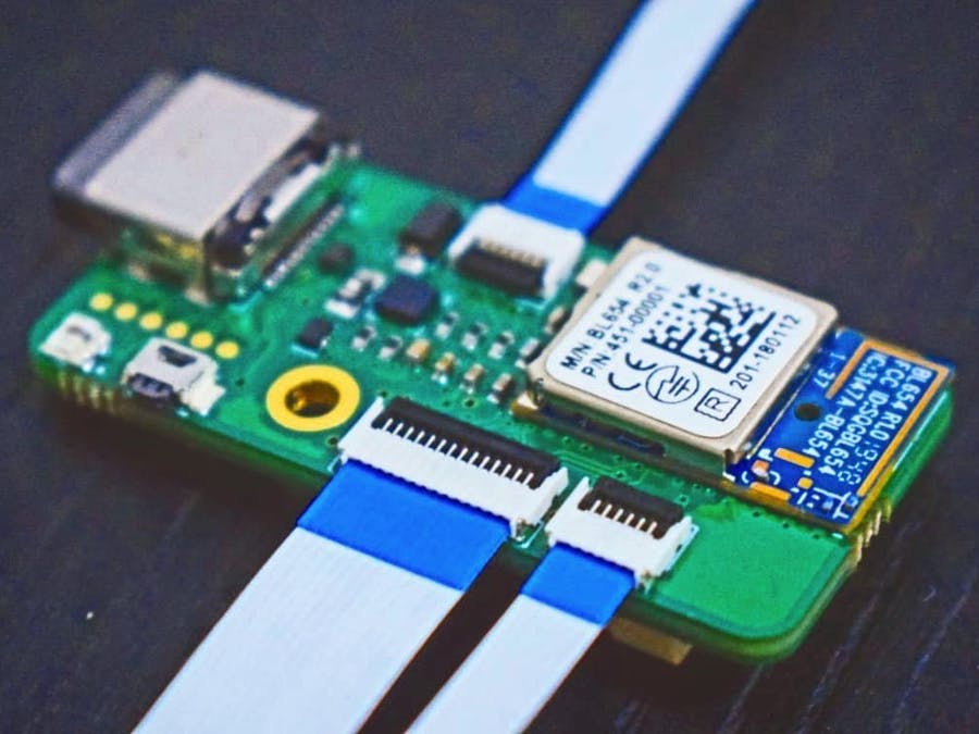
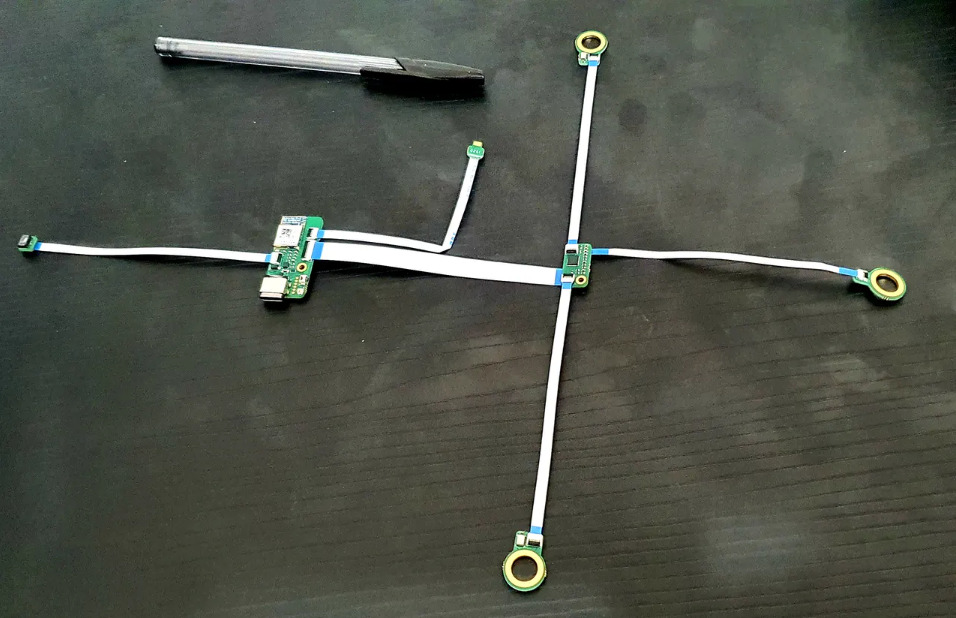
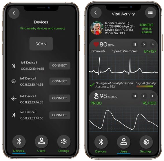
Covid-19 has inspired hundreds of health-related electronics projects from ventilators whose shortage was the initial worry for health professionals across the world to “basic” vital monitoring which was discovered to be very useful along the line. One of many projects which had remarkable engineering quality and huge potential in terms of application is the Life Data Link Monitor developed by team Horizon Medical comprising of hackster users; Jose Granados and Docomar01.
An open-source, low-cost, AI-enabled vital signs monitor designed to help manage the health status of COVID-19 patients, the Life Monitor was created to provide an innovative way for doctors to assess vital signs of thousands of patients via an AI-enabled IoT platform, to reduce the stress level of doctors and their contact with infected patients while ensuring the patients are monitored and get the best care possible.
The Life Monitor makes use of up to 7 low-cost and small, wearable medical sensors that monitor parameters like; ECG, SpO2, Temperature,Heart Rate, Respiration Rate, accelerometer (activity and fall detection), estimated Blood Pressure, and pulmonary sounds and coughing (which is achieved via a lungs microphone). The device connects to a gateway which could be a phone, tablet, or a headless server via Bluetooth 5. The data is also securely transmitted to a cloud-based platform that leverages the power of the cloud and edge computing-based AI to draw inferences that help detect and manage worsening conditions of COVID patients.
Some features and specifications of the device include:
1 channel electrocardiography (ECG, also known as EKG) compatible with snap-type electrodes.
Respiration Rate (RR) measurement.
Photoplethysmography (PPG) and Oxygen Saturation (SpO2%) monitoring.
Temperature measure.
Activity and Fall detection.
Cough counting.
Systolic and Diastolic Blood Pressure Estimation (by firmware).
Rechargeable battery connector.
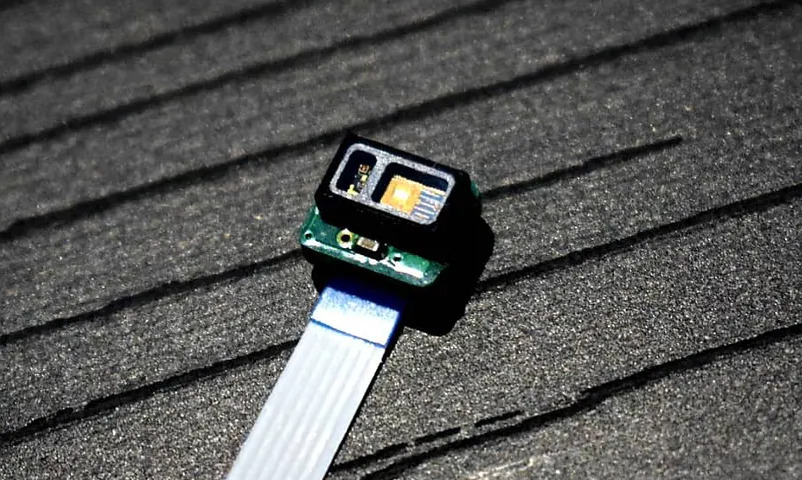
To facilitate easy development and configuration based on the needs of each patient, the project is totally modular, with the sensors connected to the mainboard via ribbon connectors, ensuring that all parts can be disassembled and assembled as needed. While a complete BOM is provided in the project documentation on hackster some of the main sensing elements used include:
ADS1292R for ECG and Respiration.
MAX30102 for PPG and SpO2.
TMP117 for ±0.1°C accurate temperature.
IIS2DLPC 3-axis accelerometer for activity and fall detection.
Dual ICS-43434 MEMS microphone
To ensure the timely response goals of the project was realized, the team also developed a companion app that makes it easy for doctors and caregivers to access the Life Monitor and get the vitals of patients.
As mentioned earlier, the project is completely open-source and everything required to replicate it, from schematics to Firmware and PCB designs are available on the Project’s Hackster page.
While it has become a norm for embedded firmware developers, tinkerers, and DIY electronics hobbyists to have multiple adapters for different communication protocols, the challenges associated with moving around with all the adapters can be quite the drag. The new Binho Nova Adapter is trying to change this by serving as a Multi-Protocol USB Host adapter, that allows users to connect I2C, SPI, 1-WIRE, and SWI devices (from sensors to microcontrollers, etc.) to computers over USB.
The device features 5 different signal pins, which in IO mode can be used varying functions like Digital Input, Digital Output, PWM Output, Digital Interrupt (on the rising edge, falling edge, or change), Analog Input, or Analog Output. Along with the 5 pins, then it also features a 3v3 pin, 1 VUSB pin, and 3 GND pins, all packed on a 10pin wire harness that terminates with a female 1.27mm 2×5 IDC connector.
Ideal for tasks like manual testing during firmware development, debugging, and automated hardware testing and validation. The pins on the Binho USB adapter can be used to communicate with any device on several digital buses like; I2C, SPI, UART, (Dallas)1-Wire, and (Atmel) Single-Wire Interface. While in the mode of operation that involves any of these protocols, the remaining pins, among the five(5), can be assigned to other related or unrelated purposes such as gpio, interrupts, chip selects, PWM signals, or analog input or outputs.
Some highlight features and specification of the adapter include:
Support for SPI @ 12MHz max clock
Support for I2C @ 3.4MHz max clock
Support for UART @ 1000000 max baud
Support for Dallas 1-Wire
Support for Atmel Single-Wire Interface
Provides 3v3 and VUSB power rails
1 x DAC Output, 5 x ADC Inputs
GPIO / Interrupt / PWM Support
Programmable RGB Status LED
Field-Upgradeable Device Firmware
Cross-platform Support for Windows, Mac, Linux
Robust, low-profile Aluminum Enclosure
USB Type-C Connector
A common use-case of the bingo adapter in production environments is for EEPROM/Flash Memory programming but it has also proven to be a lifesaver to users across related applications like;
Firmware Development
Proof of Concept Development
System Debugging
Automated Hardware Testing
Automated Firmware Testing
EEPROM Programming
FLASH Programming
FRAM Programming
The Adapter is currently available on Tindie for $149, and it ships in a package comprising a breadboard breakout adapter and a 1 foot USB type C (male) to type A (male) cable, all enclosed in a soft-shell zippered case.
More information on the product, price, and general availability can be obtained from the product’s page on Tindie.