At the heart of any embedded electronics device, either on a DIY or professional product level is a microcontroller. They run the codes/firmware that helps developers obtain inputs from sensors and tie it to actions executed through actuators. While they are usually developed as general-purpose components, MCUs are built with certain features and functionalities that make them suitable and (or) preferred by certain developers for certain applications, use cases, or scenarios. These features and functionalities have increased to meet current technological demands, making the microcontrollers not just more powerful, but more diverse, creating a selection headache for designers. Today’s article will, in no particular order, highlight the 10 most popular microcontrollers based on how often they have featured in products and the size of the communities around them.
Ready? let’s go
1. STM32F103C8T6
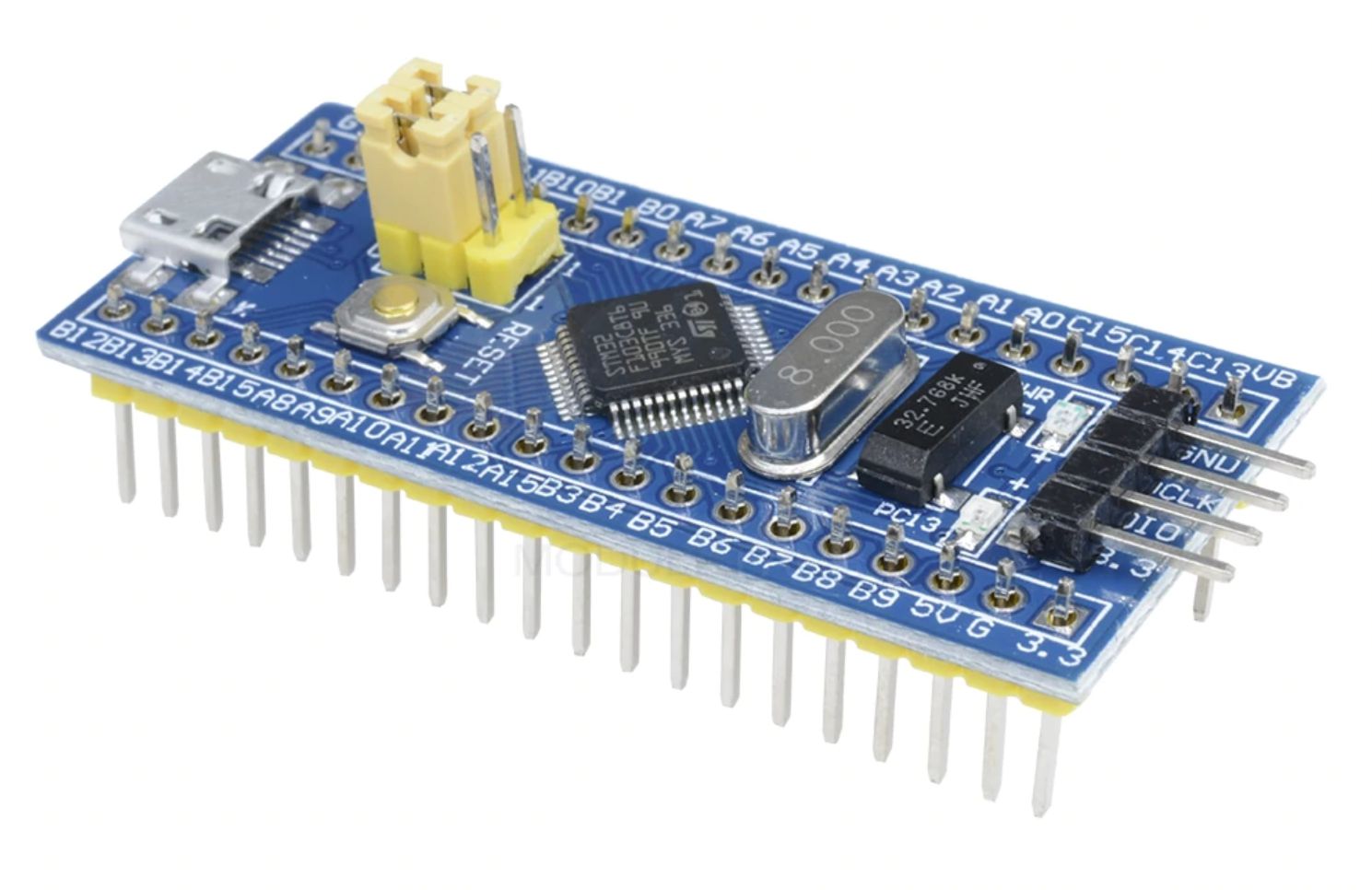
The STM32F10C8T6 is a popular member of the STM32F103xx medium-density performance line family of microcontrollers that feature a high-performance ARM® Cortex®-M3 32-bit RISC core operating at a 72 MHz frequency and possess an extensive range of enhanced I/Os and peripherals connected to two APB buses. All members of the STM32F103x family, including the CT86, offer two 12-bit ADCs, three general-purpose 16-bit timers plus one PWM timer, as well as standard and advanced communication interfaces: up to two I2Cs and SPIs, three USARTs, an USB and a CAN.
Features:
- ARM® 32-bit Cortex®-M3 CPU Core – 72 MHz maximum frequency, 1.25 DMIPS/MHz (Dhrystone 2.1) performance at 0 wait state memory access – Single-cycle multiplication and hardware division
- Memories
- 64 or 128 Kbytes of Flash memory
- 20 Kbytes of SRAM
- Clock, reset and supply management
- 2.0 to 3.6 V application supply and I/Os
- POR, PDR, and programmable voltage detector (PVD)
- 4-to-16 MHz crystal oscillator
- Internal 8 MHz factory-trimmed RC
- Internal 40 kHz RC – PLL for CPU clock
- 32 kHz oscillator for RTC with calibration
- Low-power Sleep, Stop and Standby modes
- VBAT supply for RTC and backup registers
- 2 x 12-bit, 1 µs A/D converters (up to 16 channels)
- Conversion range: 0 to 3.6 V
- Dual-sample and hold capability
- Temperature sensor
- DMA
- 7-channel DMA controller
- Peripherals supported: timers, ADC, SPIs, I 2Cs and USARTs
- Up to 80 fast I/O ports
- 26/37/51/80 I/Os, all mappable on 16 external interrupt vectors and almost all 5 V-tolerant
- Debug mode – Serial wire debug (SWD) & JTAG interfaces
- 7 timers
- Three 16-bit timers, each with up to 4 IC/OC/PWM or pulse counter and quadrature (incremental) encoder input
- 16-bit, motor control PWM timer with deadtime generation and emergency stop
- 2 watchdog timers (Independent and Window)
- SysTick timer 24-bit down counter
- Up to 9 communication interfaces – Up to 2 x I2C interfaces (SMBus/PMBus)
- Up to 3 USARTs (ISO 7816 interface, LIN, IrDA capability, modem control)
- Up to 2 SPIs (18 Mbit/s)
- CAN interface (2.0B Active)
- USB 2.0 full-speed interface
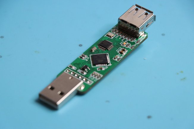
Development Boards based on MCU:
- Blue Pill
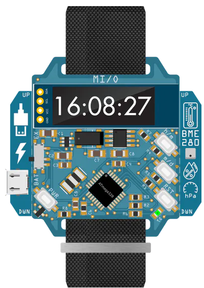
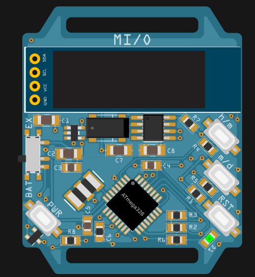
2. ATmega328
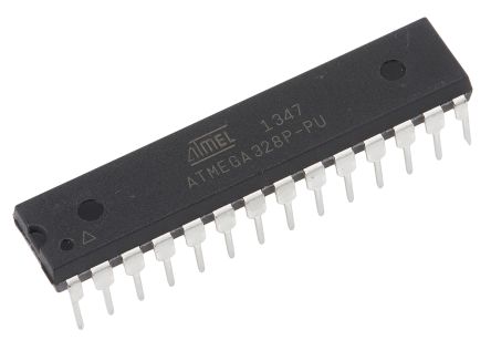
Arguably one of the most popular microcontrollers in the world, the Atmega328p has been the microcontroller of choice to a lot of designers who want to avoid the bulkiness of the Arduino boards, but retain the ease of programming, community support, and other amazing features associated with the Arduino development platform. It’s an 8-bit AVR microcontroller based on an advanced RISC architecture and combines 32KB ISP flash memory with read-while-write capabilities.
Features:
1KB EEPROM, 2KB SRAM, 23 general purpose I/O lines, 32 general purpose working registers, three flexible timer/counters with compare modes, internal and external interrupts,serial programmable USART, a byte-oriented 2-wire serial interface, SPI serial port, 6-channel 10-bit A/D converter (8-channels in TQFP and QFN/MLF packages), and
- Program Memory – 32KB (Flash)
- CPU Speed (MIPS/DMIPS) – 20
- 1KB EEPROM
- Digital Communication Peripherals – 1-UART, 2-SPI, 1-I2C
- 2KB SRAM
- 23 GPIO
- 6-channel 10-bit A/D converter (8-channels in TQFP and QFN/MLF packages)
- 5 software selectable power saving modes
- 3 builtin Timers with compare modes – 2 8bit and 1 16bit
- PWM pins – 6
- programmable watchdog timer with internal oscillator
- 32 general-purpose working registers,
Development Boards Based on MCU:
- Arduino Nano
- Arduino UNO
- Arduino Pro Mini
- Sparkfun Redboard
- A host of other Arduino Clones
Standout Features:
- Express Compatibility with the Arduino Development platform
- Large community support due to relationship with Arduino
3. PIC16F877A
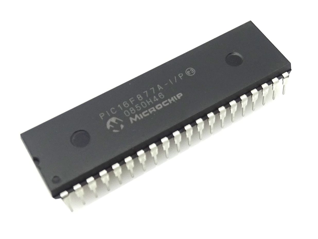
The PIC16F877A is arguably the most popular 8-bit microcontroller in the PIC family of MCUs. While it’s considered by some as old and past its time, the PIC16F877A is no doubt, still one of the most popular microcontrollers in the world. It is seen as the de-facto microcontroller for beginners looking to get into embedded development with PIC and it ends up as the microcontroller of choice for them when they become experts.
Features:
Some features of the PIC16F877A are provided below:
- Total number of Pins – 40
- Total number of ports – 5 (port A, port B, port C, port D, port E)
- Operating Voltage – 2 to 5.5V
- Number of input/output pins – 33
- Number of ADC pins – 14
- ADC Resolution – 10-bit
- Number of Comparators – 2
- Number of timers – 3
- Communication protocols – UART, SPI, I2C
- External Oscillator – up to 20Mhz
- Program Memory – 14KB
- RAM – 368 bytes
- EEPROM – 256 bytes
- Max PWM resolution – 10
- Support both hardware pin and timer interrupts
Development Boards Based on MCU:
- The PIC Development board
Dev boards are one of the reasons why PIC microcontrollers are increasingly becoming unpopular. While the PIC development boards are usually very good for beginners because they come with different components that aids learning, for the average designer, they are considered bulky and pretty much uninteresting to work with, as most of the components included are usually not needed by experienced designers.
4. Attiny85
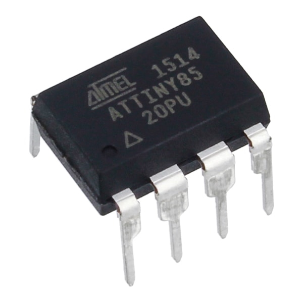
Loved for their tiny form-factor, the ATtiny series of microcontrollers are considered as the go-to microcontroller for projects where a small form factor is desired, and the number of GPIOs required is low. Of all the microcontrollers in this series, the aTtiny85 is regarded as the most popular, presumably because it seems to have more I/O pins compared to others. While Microchip announced a new range of ATtiny chips with significant performance upgrades, the ATtiny85 is still revered, mostly because of the familiarity most designers have built with it over time.
Features:
Some features of the ATtiny85 include:
- Total number of pins – 8
- CPU type – RISC 8-Bit AVR
- Operating Voltage – 1.8 – 5.5V
- Program Memory – 8K
- RAM Memory – 512Bytes
- EEPROM Memory – 512Bytes
- ADC Resolution – 10-Bit
- Number of ADC pins – 4
- Number of Comparators – 1
- GPIO’s – 6
- No of Timers – 2 8-bit timers
- Communication Protocols- SPI, I2C, and USART.
- Number of PWM pins – 4
- Maximum oscillator speed – Up to 20MHz
Development Boards Based on MCU:
- Mini ATtiny85 USB
- Digispark ATtiny85
Standout Features:
Stand out feature for the ATtiny85 will be their small form-factor and their relatively low power consumption features.
5. MSP430G2452
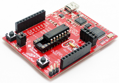
The MSP430 family of microcontrollers from TI are considered as some of the most modern microcontrollers and the most popular member of that family so far has been the MSP430G2452. The MSP430G2452 is a powerful, and relatively cheap microcontroller based on a 16-bit RISC CPU manufactured by Texas Instruments.
Features:
Some features of the MCU include:
- Number of Comparator channels – 8
- ADC channels – 8
- Number of GPIO’s pins – 16
- ADC Resolution – 10-Bit SAR
- Number of Timers – 1 (16-bit)
- Non-Volatile Memory – 8kB
- Communication protocols – 1 I2C, 1 SPI
- Low Supply Voltage Range – 1.8V – 3.6V
- Low-Frequency Oscillator-32-kHz Crystal and also external Digital Clock Source
- SRAM – 256B
- Active Mode Power consumption – 220microA at 1MHz
Development Boards Based on MCU:
- MSP-EXP430G2 LaunchPad TI Development Board
Standout Features:
The MSP430 series of microcontrollers are famous for their low power features.
6. ESP8266
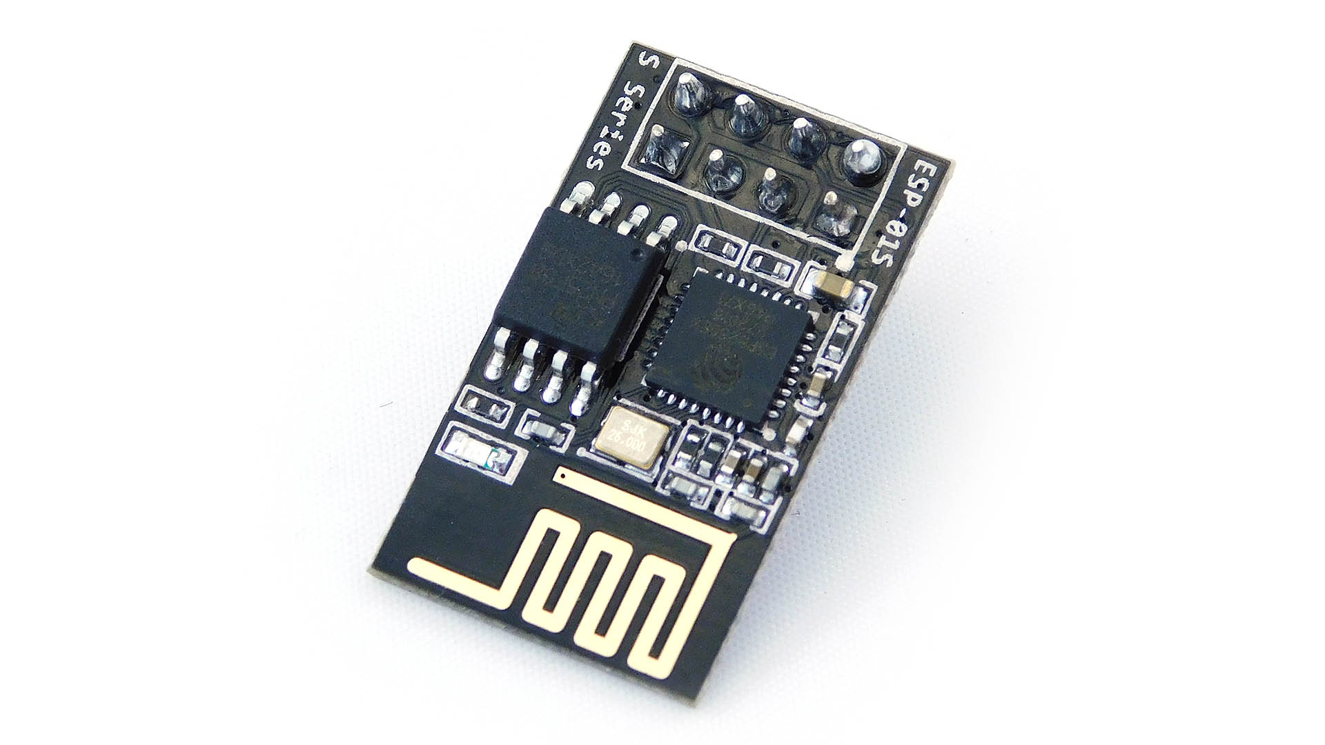
The popularity of the ESP8266 cannot be contested. It is unarguably one of the most impactful microcontrollers of the last decade and it definitely was one of the pacesetters for the current trend of microcontrollers with fused communication capabilities. Developed by Espressif Systems, the ESP8266 is a low-cost Wi-Fi microchip, with a full TCP/IP stack and microcontroller capability. Multiple versions of the MCU were created in quick succession and what started initially as a Wi-Fi module for microcontrollers quickly spurned off to a module like the ESP-12e which became the heart of several projects and products.
Features:
- Processor: L106 32-bit RISC microprocessor core based on the Tensilica Xtensa Diamond Standard 106Micro running at 80 MHz
- Memory:
- 32 KiB instruction RAM
- 32 KiB instruction cache RAM
- 80 KiB user-data RAM
- 16 KiB ETS system-data RAM
- External QSPI flash: up to 16 MiB is supported (512 KiB to 4 MiB typically included)
- IEEE 802.11 b/g/n Wi-Fi
- Integrated TR switch, balun, LNA, power amplifier and matching network
- WEP or WPA/WPA2 authentication, or open networks
- 16 GPIO pins
- SPI
- I²C (software implementation)
- I²S interfaces with DMA (sharing pins with GPIO)
- UART on dedicated pins, plus a transmit-only UART can be enabled on GPIO2
- 10-bit ADC (successive approximation ADC)
Development Boards Based on MCU:
There are over 100 development boards based on the different variations of the ESP8266. To mention a few, some of these boards include;
- NodeMCU DevkIT
- Wemos D1
- Wemos D1 Mini
- Adafruit Feather HUZZAH ESP8266
- SparkFun ESP8266 Thing
Standout Features:
Some standout features of the ESP8266 includes;
- Integrated WiFI and Microcontroller reduces BOM and sourcing related headaches
- Low cost
- pre-certified (FCC and CE)
- large Community support
- Compatibility with popular Platforms like the Arduino IDE
7. ESP32
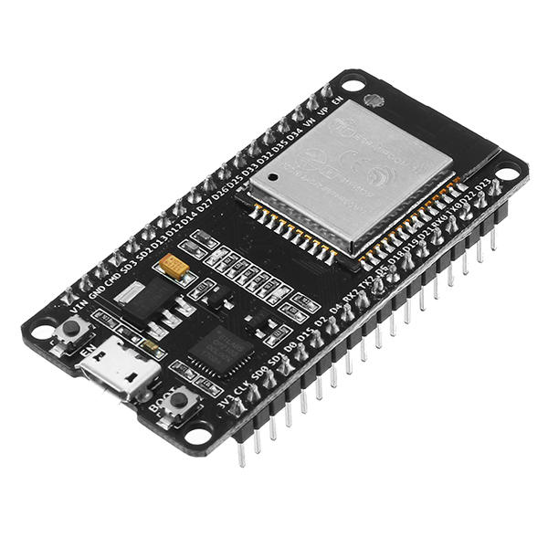
An upgrade to the ESP8266, the esp32 has enjoyed great support and adoption since its release few years back. it is a low-cost, low-power system on a chip microcontroller with integrated Wi-Fi and dual-mode Bluetooth. it uses the Tensilica Xtensa LX6 microprocessor in both dual-core and single-core variations and includes built-in antenna switches, RF balun, power amplifier, low-noise receive amplifier, filters, and power management modules. Designed for modern applications, ESP32 also incorporates several security features like Cryptographic hardware acceleration, flash encryption, and secure boot.
Features:
Some features of the MCU include:
- Processors:
- CPU: Xtensa dual-core (or single-core) 32-bit LX6 microprocessor, operating at 160 or 240 MHz and performing at up to 600 DMIPS
- Ultra-low power (ULP) co-processor
- Memory: 520 KiB SRAM
- Wireless connectivity:
- Wi-Fi: 802.11 b/g/n
- Bluetooth: v4.2 BR/EDR and BLE (shares the radio with Wi-Fi)
- Peripheral interfaces:
- 12-bit SAR ADC up to 18 channels
- 2 × 8-bit DACs
- 10 × touch sensors (capacitive sensing GPIOs)
- 4 × SPI
- 2 × I²S interfaces
- 2 × I²C interfaces
- 3 × UART
- SD/SDIO/CE-ATA/MMC/eMMC host controller
- SDIO/SPI slave controller
- Ethernet MAC interface with dedicated DMA and IEEE 1588 Precision Time Protocol support
- CAN bus 2.0
- Infrared remote controller (TX/RX, up to 8 channels)
- Motor PWM
- LED PWM (up to 16 channels)
- Hall effect sensor
- Ultra-low-power analog pre-amplifier
- Security:
- IEEE 802.11 standard security features all supported, including WFA, WPA/WPA2 and WAPI
- Secure boot
- Flash encryption
- 1024-bit OTP, up to 768-bit for customers
- Cryptographic hardware acceleration: AES, SHA-2, RSA, elliptic curve cryptography (ECC), random number generator (RNG)
- Power management:
- Internal low-dropout regulator
- Individual power domain for RTC
- 5μA deep sleep current
- Wake up from GPIO interrupt, timer, ADC measurements, capacitive touch sensor interrupt
Development Boards Based on MCU:
Like the ESP8266 there are a lot of development boards based on the ESP32. Some of these boards include;
- HUZZAH32
- ESP32-DevKitC
- NodeMCU-32S
- ESPduino32
- ESP32 Thing
Standout Features:
Asides WiFi, ESP32 features Bluetooth and implements security and low power features that are not available in regular devices.
8. ATMEGA32U4
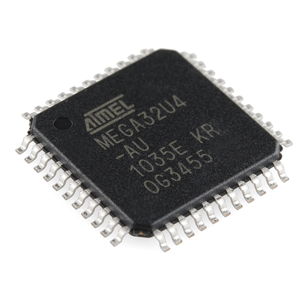
The Atmega32u4 is a low-power Microchip 8-bit AVR® RISC-based microcontroller featuring 32 KB self-programming flash program memory, 2.5 KB SRAM, 1 KB EEPROM, USB 2.0 full-speed/low-speed device, 12-channel 10-bit A/D-converter, and JTAG interface for on-chip-debug. The device is able to execute powerful instructions in a single clock cycle, enabling it to achieve up to 16 MIPS throughput at 16 MHz. This gives designers the ability to optimize power consumption versus processing speed.
Features:
- Complies fully with Universal Serial Bus Specification Rev. 2.0
- Supports data transfer rates up to 12 Mbit/s and 1.5 Mbit/s
- Endpoint 0 for Control Transfers: Up to 64 bytes
- Six Programmable Endpoints with In or Out Directions and with Bulk, Interrupt or Isochronous Transfers
- Configurable Endpoints size up to 256 bytes in double bank mode
- Fully independent 832 bytes USB DPRAM for endpoint memory allocation
- Suspend/Resume Interrupts
- CPU Reset possible on USB Bus Reset detection
- 48 MHz from PLL for Full-Speed Bus Operation
- USB Bus Connection/Disconnection on Microcontroller Request
- A crystal-less operation for Low-Speed mode
Development Boards Based on MCU:
The Atmega32u4 is a popular microcontroller and is featured in several development boards some which include;
- Teensy 2.0
- Arduino Beetle
- Arduino Pro Micro
- Arduino Leonardo
- Qwicc Pro
- Arduino Leonardo Clones
9. STM8S103F3
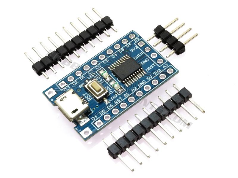
The STM8 family of microcontrollers offers a high-performance 8-bit core and a state-of-the-art set of peripherals in a tiny form factor, similar to what is obtainable with the ATtiny series of MCUs. The family is made up of 4 series including; the STM8S, the STM8L, the STM8AF, and the STM8AL. Of all these, the STM8S series is considered to be the mainstream MCU and the STM8S103F3 is considered to be one of the most popular MCUs in the Series.
The 8-bit microcontroller offers 8 Kbyte Flash program memory, with an integrated true data EEPROM, advanced core and peripherals, a 16 MHz clock frequency, robust I/Os, independent watchdogs with separate clock source, and a clock security system, all of which ensures its high performance and overall system robustness.
Features:
Highlight features of the microcontroller, according to the datasheet include:
- Core
- 16 MHz advanced STM8 core with Harvard architecture and 3-stage pipeline
- Extended instruction set
- Memories
- Program memory: 8 Kbyte Flash; data retention 20 years at 55 °C after 10 kcycle
- Data memory: 640 byte true data EEPROM; endurance 300 kcycle
- RAM: 1 Kbyte
- Clock, reset and supply management
- 2.95 to 5.5 V operating voltage
- Flexible clock control, 4 master clock sources
- Low power crystal resonator oscillator
- External clock input
- Internal, user-trimmable 16 MHz RC
- Internal low-power 128 kHz RC
- Clock security system with clock monitor
- Power management:
- Low-power modes (wait, active-halt, halt)
- Switch-off peripheral clocks individually
- Permanently active, low-consumption power-on and power-down reset
- Interrupt management
- Nested interrupt controller with 32 interrupts
- Up to 27 external interrupts on 6 vectors
- Timers
- Advanced control timer: 16-bit, 4 CAPCOM channels, 3 complementary outputs, dead-time insertion and flexible synchronization
- 16-bit general purpose timer, with 3 CAPCOM channels (IC, OC or PWM)
- 8-bit basic timer with 8-bit prescaler
- Auto wake-up timer
- Window watchdog and independent watchdog timers
- Communication interfaces
- UART with clock output for synchronous operation, SmartCard, IrDA, LIN master mode
- SPI interface up to 8 Mbit/s
- I2C interface up to 400 kbit/s
- Analog to digital converter (ADC)
- 10-bit, ±1 LSB ADC with up to 5 multiplexed channels, scan mode and analog watchdog
- I/Os
- Up to 28 I/Os on a 32-pin package including 21 high sink outputs
- Highly robust I/O design, immune against current injection
- Unique ID
- 96-bit unique key for each device
Development boards Based on Microcontroller:
There are a lot of breakout boards based on the STM8S103F3 microcontroller that are not sophisticated enough to be classified as a development board. Some noteworthy boards based on the MCU include;
- Sduino / STM8Blue and similar clones
- STM8S103F3 P6 Development Board
10. NXP LPC1768
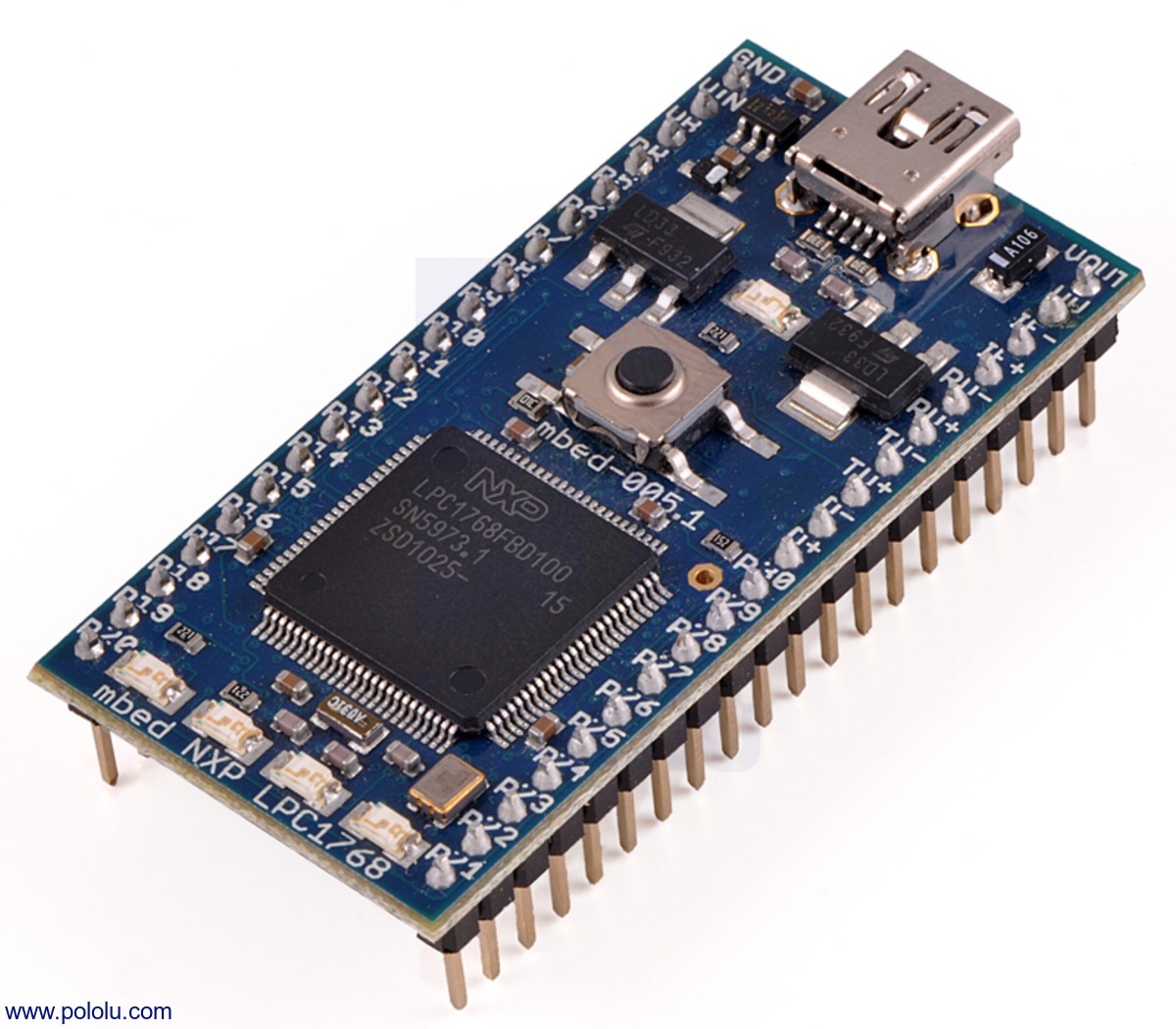
The LPC1768 is a Cortex®-M3 microcontroller designed for embedded applications with low power requirements. It features a high level of integration and low power consumption at frequencies of up to 100 MHz. It’s is a high-performance microcontroller and features up to 512 kB of flash memory and 64 kB of data memory, along with peripherals like an Ethernet MAC, a USB Device/Host/OTG interface, 8-channel DMA controller and 4 UARTs, among others.
Features
Some highlight features of the NXP LPC1768 includes:
- Arm® Cortex-M3 processor, running at frequencies of up to 100 MHz
- Arm Cortex-M3 built-in Nested Vectored Interrupt Controller (NVIC)
- Up to 512 kB on-chip flash programming memory
- Up to 64 kB On-chip SRAM
- In-System Programming (ISP) and In-Application Programming (IAP)
- Eight channel General Purpose DMA controller (GPDMA)
- Ethernet MAC with RMII interface and dedicated DMA controller
- USB 2.0 full-speed device/Host/OTG controller
- Four UARTs with fractional baud rate generation, internal FIFO, and DMA support
- CAN 2.0B controller with two channels
- SPI controller with synchronous, serial, full duplex communication
- Two SSP controllers with FIFO and multi-protocol capabilities
- Three enhanced I2C bus interfaces
- I2S (Inter-IC Sound) interface
- 70 General Purpose I/O (GPIO) pins with configurable pull-up/down resistors
- 12-bit/8-ch Analog/Digital Converter (ADC) with conversion rates up to 200 kHz
- 10-bit Digital/Analog Converter (DAC) with dedicated conversion timer and DMA
- Four general purpose timers/counters
- One motor control PWM with support for three-phase motor control
- Quadrature encoder interface that can monitor one external quadrature encoder
- One standard PWM/timer block with external count input
- Low power RTC with a separate power domain and dedicated oscillator
- WatchDog Timer (WDT)
- Arm Cortex-M3 system tick timer, including an external clock input option
- Repetitive interrupt timer provides programmable and repeating timed interrupts
- Each peripheral has its own clock divider for further power savings
- Standard JTAG test/debug interface for compatibility with existing tools
- Integrated PMU (Power Management Unit)
- Four reduced power modes: Sleep, Deep-sleep, Power-down, and Deep power-down
- Single 3.3 V power supply (2.4 V to 3.6 V)
- Four external interrupt inputs configurable as edge/level sensitive
- Non-maskable Interrupt (NMI) input
- Wake-up Interrupt Controller (WIC)
- Processor wake-up from Power-down mode via any interrupt
- Brownout detect with separate threshold for interrupt and forced reset
- Power-On Reset (POR)
- Crystal oscillator with an operating range of 1 MHz to 25 MHz
- 4 MHz internal RC oscillator trimmed to 1 % accuracy
- Code Read Protection (CRP) with different security levels
- Unique device serial number for identification purposes
Development Boards:
Top development boards based on the NXP LPC1768 include;
- Arm Mbed LPC1768 Board
- Keil LPC1769 Evaluation Board
- LPCXpresso board for LPC1769 with CMSIS DAP probe
With 1000s of microcontrollers in existence, there are definitely a few other microcontrollers out there that probably deserve a spot on this list, but you will agree with me that the community, projects, and products that have been built around the MCUs featured in these articles are hard to match.
What are your thoughts? what other microcontrollers do you think should have made this list? Feel free to share via the comment section.