RA4W1 – 48MHz Bluetooth® 5.0 Low Energy Single Chip MCU from RA4 Series

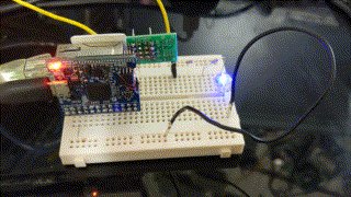
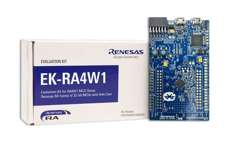
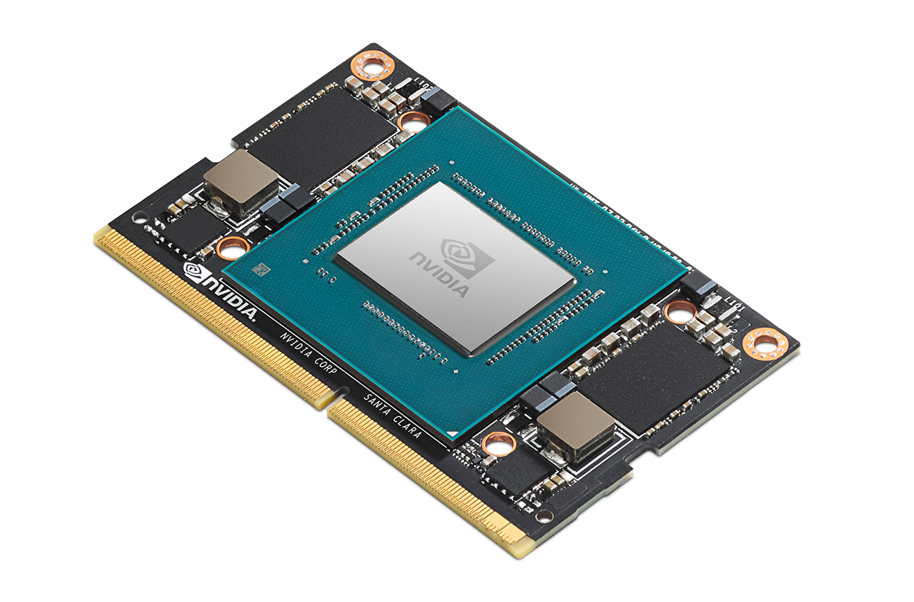
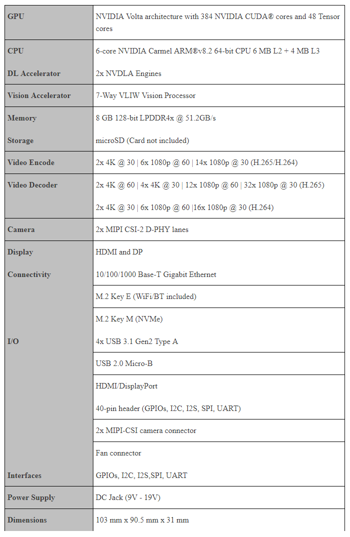
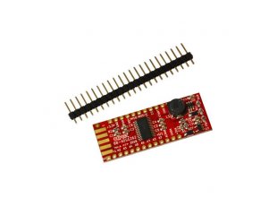
The Renesas RA4W1 is the first Bluetooth 5.0 Low Energy fully compliant with 2Mbit High-Throughput (HT) and Long Range (LR) support in a single chip MCU of Renesas RA4 product series for IoT applications that require a high-performance Arm® Cortex®-M4 core at a very attractive price point. The RA4W1 is built on a highly efficient low power process and is supported by an open and flexible ecosystem concept, called Flexible Software Package (FSP), using FreeRTOS as base. RA4W1 is geared towards IoT application requiring Security, large embedded RAM and low power consumption.

Key features

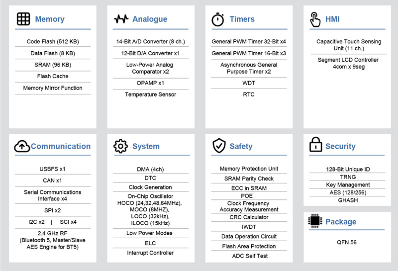
  • 48MHz Arm® Cortex®-M4
  • 512kB Flash Memory and 96kB SRAM
  • 8kB DataFlash to store data as in EEPROM
  • 7x7mm QFN 56 pin package.
  • Capacitive Touch Sensing Unit
  • Segment LCD Controller
  • USBFS 2.0 Full Speed (Host/Device) CAN 2.0B
  • SCI (UART, Simple SPI, Simple I2C)
  • SPI/ I2C Multimaster Interface
  • 2.4 GHz radio with Bluetooth 5.0 Low Energy
  • Advertising Extension and Long Range support
  • Secure Crypto Engine (AES128 / 256, GHASH, TRNG)

Benefits

  • Full functionality of Bluetooth 5.0 Low Energy along with the high-performance processing and superior power efficiency.
    • High Throughput and Long Range support
  • Integrated Secure Crypto Engine with several cryptography accelerators and Key management.
  • Large 96kB embedded SRAM suitable for handling communication stacks.

Applications

  • Security (Fire Detection, Burglar Detection, Panel control)
  • Metering (Electricity, Automated Meter Reading)
  • Industry (Robotics, Door Openers, Sewing Machines, Vending machines, UPS)
  • Health and Wearables Body Sensors
  • Smart Home and Remote Control Toys

more information: www.renesas.com

A Simple Miniature Digital Storage Oscilloscope powered by an STC MCU

For makers and electronics engineers, the oscilloscope is one of the most important tools in the lab. It is a test instrument for visualizing and observing various signals usually as a two-dimensional plot of signals against time. Apart from being used to view and compare waveforms in the design and debugging of electronic systems, the oscilloscope is also very useful in determine voltage levels, frequencies, and other signal parameters as they change with time. However, most of the oscilloscopes available today are quite expensive, be it small or advanced.

In a bid to make things easier, several projects are beginning to show up on how someone, with the right tools, can create cheap and compact oscilloscope that will do the job for hobby tasks. One of such is CreativeLau’s build that puts a tiny Digital Storage Oscilloscope within your reach.

Following an earlier release on how to make an STC-powered function generator on his YouTube channel, maker Creative Lau has published another DIY guide, this time on how to easily build a simple miniature digital storage oscilloscope with a DIP-packaged STC8A8K64S4A12 microcontroller unit for basic engineering needs.

“This is a simple oscilloscope made with STC MCU. You can use this Mini DSO to observe waveforms with a time interval of 100us – 500ms, the voltage range of 0-30V, and a draw mode of vector or dots” says Lau as he writes about his project.”

Lau’s build goes hand in hand with the STC-powered function generator. It is simple, cheap, and easy to assemble. The only limit is that it is still unable to read voltages lower than zero; it’s readings automatically stop at zero no matter how low the voltage goes.

Video

Apart from the STC8A8K64S4A12 microcontroller, the other components used for the build include a compact SSD1306 OLED display, a 5V booster module, one 3.7V Li-ion battery pack for portability as well as a rotary EC11 encoder and Tact switch for user interface and power on/off. Others include one four resistors and two capacitors (47uF and 0.01uF).

Meanwhile, Lau claims that the build is still being worked on and hopes to share updates on it as soon as he is done.

“The new functions for the Mini DSO are being developed. They are Normal Sweep and Single Sweep. With these functions, you could observe the waveform mutation” Lau explains.

More details of this build can be found on Instructables including the schematics and circuit design attached under the download section of the site.

NVIDIA® Jetson Xavier™ NX Developer Kit

The NVIDIA® Jetson Xavier™ NX Developer Kit brings supercomputer performance to the edge. It includes a power-efficient, compact Jetson Xavier NX module for AI edge devices. It benefits from new cloud-native support and accelerates the NVIDIA software stack in as little as 10 W with more than 10X the performance of its widely adopted predecessor, Jetson TX2. The capability to develop and test power-efficient, small form-factor solutions with accurate, multi-modal AI inference opens the door for new breakthrough products.

Developers can now take advantage of cloud-native support, transforming the experience of developing and deploying AI software to edge devices. Pre-trained AI models from NVIDIA NGC, together with the NVIDIA Transfer Learning Toolkit, give a faster path to trained and optimized AI networks. Containerized deployment to Jetson devices also allows flexible and seamless updates.

The developer kit is supported by the entire NVIDIA software stack, including accelerated SDKs and the latest NVIDIA tools for application development and optimization. When combined with the compact Jetson Xavier NX, this powerful stack helps you create innovative solutions for smart cities, retail, manufacturing, logistics, healthcare, agriculture, and more.

Designed for ease of use and speed of deployment, Jetson is the most flexible platform to get to market and continuously update over the lifetime of a product.

Features

  • Compact size Jetson Xavier NX module powerful enough for advanced AI applications with low power consumption
  • Supports Entire NVIDIA Software Stack for application development and optimization
  • Rich I/O Peripherals to further expand AI projects
  • Onboard Fan to provide better heat dissipation
  • More than 10X the performance of Jetson TX2
  • Enables development of AI applications using NVIDIA JetPack™ SDK
  • Easy to build, deploy, and manage AI at the edge
  • Flexible and scalable platform to get to market with reduced development costs
  • Continuous updates over the lifetime of the product

Specifications

NVIDIA® Jetson Xavier™ NX Developer Kit is on sale for $399 and can be pre-ordered now on SeeedStudio.

DIY Silicon Photodiode Particle Detector directly from CERN

Silicon detectors are widely used in particle and nuclear physics for measuring ionizing radiation. This Do-It-Yourself project allows making a low-cost particle detector from scratch using silicon photodiodes. It can distinguish different particle types (alpha particles and electrons) and measures their energy between 33 keV and 8 MeV. The detector must be shielded from light and is, therefore, best mounted inside your favorite candy tin box. The signal output can be directly connected with microphone or headset inputs of regular laptops and smartphones.

The DIY particle detector is open source science hardware, released under the CERN open hardware license. Construction details and software for undertaking measurements can be found on the corresponding project website. The circuit board and electronic parts (~20 EUR) can be easily procured via kitspace, an open hardware design repository.

DIY Silicon Photodiode Particle Detector directly from CERN – [Link]

Latest Olimex board brings 10-channel 32-bit to OSHW builds

If your project demands some high precision analog measurements, then here is a new Olimex BB-ADS1262 that can help get the job done easily; with up to 10 channels of 32-bit ADC conversion, the new BB-AD S1262 breakout board is considered a great add-on for microcontrollers.

Before, system designers who needed a high-resolution analog-to-digital-converter have to sacrifice certain desired specifications like low noise, low offset drift, and several other integrated features. Things have however become easier as there are now ADCs that have helped to eliminate these trade-offs by providing a high resolution alongside fault-detection features, faster data rates, and wider temperature range, thereby maximizing performance.

The new BB-ADS1262 from Olimex is built around the Texas Instrument ADS1262 ADC chip and offers up to 10 Channel low-noise low-drive 32-bit ADC on an Open-source hardware breakout board.

“The BB-ADS1262 is a breakout board for the ADS1262 low-noise, low-drift 38.4 KSPS, delta-sigma ADCs with an integrated PGA (Programmable Gain Amplifier), reference, and internal faults monitors. Possible applications are sensor reading, small signals (ECG / EEG), weight scales, strain gauge sensors, thermocouples, and resistance temperature devices (RTDs).”

says the Bulgarian open source specialist as he launches his new design.

The 10 channel sigma-delta precise 32 bit ADC breakout board is fully open source according to the Open Source Hardware definition and licensed under the CERN – Open Hardware Licence Version 2.0; software is released under the GPL3 Licensee (including an Arduino demo code) while the documentation is under a CC BY SA 3.0.

Designed for high accuracy and stability, the BB-ADS1262 breakout board has some key features worth taking note of, including;

  • Up to 32-bit ADC conversion precision
  • Data rates of 2.5 samples per second to up to 38,400 samples per second
  • An offset drift of 1 nV / 0C and a gain drift of 0.5 ppm / 0C
  • CMOS programmable gain amplifier plus Differential Input
  • Noise level: 7 nVRMS (2.5 samples per second with the gain set to 32)
  • 50 Hz and 60 Hz Rejection
  • Internal voltage reference: 2.5V
  • Linearity: 3 parts per million and,
  • 47 x 18 mm ( 1.85 x 0.7 inch) in size

The BB-ADS1262 board currently sells at $28, precisely €25.95 (with some discounts over a certain number of pieces) in Olimex’s shop. More details on it including hardware files and source codes can be found in their GitHub repository.

Newark Launches New Tektronix Digital Storage Oscilloscope

Newark has added the new entry-level TBS2000B Digital Storage Oscilloscope from Tektronix to its test and measurement portfolio.

The TBS2000B series is a complete drop-in replacement for TBS2000 series oscilloscopes, with the same form factor and programmable interface.

Features of the TBS2000B include:

  • A 9-inch WVGA display with a 5-million-point record length and 2GS/s sample rate which enables users to capture and display more signal, speeding up debug, and design validation.
  • 32 automated measurements and on-waveform cursor readouts with search and mark features that enable identification of events that occur in the acquired waveform.
  • TekVPI, Tektronix’s proprietary probe support interface, enabling application coverage using the latest active differential and current probes with automatic scaling and units. This is the industry’s only entry-level instrument featuring TekVPI, according to the company. The TBS2000B also supports traditional passive BNC probes.
  • Range of connectivity options including Wi-Fi support (via USB Wi-Fi dongle), 2 USB host ports, and 100-BaseT Ethernet for sharing of measurements and collaboration.

Newark offers 24/5 technical support with test and measurement specialists on-hand and online resources such Newark’s online probe selector tool.

The Tektronix TBS2000B Digital Storage Oscilloscope is available from Newark in North America.

For more information, visit: https://www.newark.com/

Analog Devices Releases Dual Silent Switcher Series

Analog Devices released the LT8650S, LT8652S and LT8653S dual-channel 4A/8.5A/2A synchronous step-down Silent Switcher® converters. The silent switcher series is based on the Silent Switcher 2 architecture, coupled with spread spectrum frequency modulation. Per the company, this ensure PCB layout robustness to achieve ultra-low EMI performance that meets CISPR25 emissions.

The outputs are able to be paralleled to scale up or down the current based on the system. This can be performed while optimizing thermal performance.

LT8650S/LT8652S/LT8653S Key Features as Provided by the Company

  • Silent Switcher 2 Technology with Integrated Bypass Capacitors meets CISPR25 Emissions
  • Ultralow Quiescent Current Burst Mode® for Light Load operation
  • Up to 12A (LT8652S) on one channel
  • Adjustable and Synchronizable Frequency (300kHz to 3MHz)

For more information, visit http://www.analog.com

BeagleBone Green Gateway SBC features Sitara AM3358, Ethernet, and a DC Jack

SeeedStudio has been working on an addition to their BeagleBone Green Development Board family with an update to the BeagleBone Green Wireless board named BeagleBone Green Gateway. The board features the new Octavo Systems OSD3358, which is a SiP (System in Package) that integrates the AM3358 1GHz ARM Cortex-A8 Processor, 512MB DDR3 SRAM, and other wonderful features into one package. 

The new board is being designed to suit applications where the board is being used as a gateway, as such, it comes with both Ethernet Connectivity, WiFi and BLE Wireless connectivity options. The board also comes with an extra DC connector for power (overcoming the Micro USB only for power limitation), and an onboard I2C RTC, so that it is more suitable for industrial application or applications where time accuracy is required.

The board is available for pre-order for 59.90 USD

Key Features

  • Fully Compatible with BeagleBone® Black and Seeed Studio BeagleBone® Green
  • Compact size for convenient deployment
  • Powerful Sitara™ AM3358 Arm® Cortex® A8 Processor
  • Rich I/O Peripherals
  • PRUs for Real-TIme Capabilities
  • Cape Support for Expandability
  • Open-Source
  • Support from the fast-growing community

Some of the expected features and specifications of the new board include;

Processor

  • Processor: Octavo Systems OSD3358
  • AM3358 1GHz ARM Cortex-A8
  • 2×32-bit 200-MHz programmable real-time units (PRUs)
  • 3D graphics accelerator
  • NEON floating-point accelerator
  • 512MB DDR3 SDRAM
  • 4KB EEPROM
  • Integrated power management

Memory

  • 4GB 8-bit eMMC onboard flash storage
  • SD/MMC Connector for microSD

Connectivity

  • DC Jack for power, 12V
  • Ethernet 10/100Mbit
  • USB 2.0 Host x2
  • USB client for power and communications
  • 2x 46 pin headers
  • 2x Grove connectors (I2C and UART)
  • WiFi 802.11 b/g/n 2.4GHz
  • Bluetooth 4.1 with BLE
  • I2C RTC, and 3V battery connector
  • Debug UART header
  • 3x Buttons
  • 2x 46 pin headers and 2x Grove connectors fully compatible with Seeed Studio Beaglebone Green and Seeed Studio Beaglebone Green Wireless
  • Operating Temperature: 0 ~ 70

The BeagleBone Green Gateway is expected to run Debian with the Cloud9 IDE just like the BeagleBone Green Wireless, and it’s price even though not yet announced by Seeed, is expected to be more than that of the BeagleBone Green Wireless due to the new features. Any thoughts/comments/ideas on the BeagleBone Green Gateway? Do share via the comment section.

more information: www.seeedstudio.com

BreadBee Tiny Embedded Linux SBC is Based On MStar MSC313E Camera SoC

We have many tiny and compact Arm Linux SBC on the market today, ranging from NanoPi NEO to Raspberry Pi Zero or Rock Pi S. However, Daniel Palmer is launching a crowdfunding campaign for the BreadBee, which is tiny, but yet fully-functional Linux-based single-board computer designed based on MStar MSC313E Cortex-A7 system-on-chip (SoC) originally aimed at IP cameras. Palmer say:

“The BreadBee is based on a relatively unknown IP camera SoC, the MSC313E, from a company called MStar.” He continues “You might have never heard of MStar but you probably have one of their chips in your TV. There are no solutions yet that can run a real OS like Linux that can be integrated by hobbyists into boards from cheap PCB vendors that don’t have show stopping limitations; i.e. the AllWinner V3s is very similar to the SoC used here but it only has one SPI controller that is lost as soon as you put SPI NOR on it… The MSC313E has just enough of the usual microcontroller peripherals to make it useful, comes in a (relatively) easy to work with QFN package, is tiny and costs ~$4. It is a bit harder to integrate into your designs than a microcontroller that requires a single power supply but all of the information you would need to do so is right here. The schematic for the BreadBee is incredibly simple.”

The Tiny BreadBee


At 32x30mm (around 1.26×1.18″) in footprint, which is smaller than any Arm Linux SBC on the market today, the compact BreadBee features a wide range of specifications. It includes a single-core 1GHz Arm Cortex-A7 with NEON instructions, 64MB of DDR2 memory, 64kB of static RAM, bootable and memory-mapped SPI-NOR, a 100Mb Ethernet port. It also includes 24-pin dual-row header (2.54mm pitch) with  SPI, I2C, 4x 10-bit ADC, 3x UART, GPIOs 21-pin header (1.27mm pitch) with SD/SDIO, USB 2.0, GPIOs, eight pulse-width modulated (PWM) pins, a real-time clock, watchdog timer, SD/SDIO interface, a USB PHY and host/device mux. The networking feature includes 10/100M Ethernet (RJ45).

The BreadBee Blinking When Performing

Some of the MSC313E‘s hardware features are not quite ready for prime-time yet. However, hardware specifications available, but as-yet unsupported features of the SoC includes the camera interface and H.264 encoder for IP camera duties, an audio ADC and DAC, hardware cryptographic acceleration, and 8051 low-power-mode management microcontroller, (somewhat like an IR decoder that can wake the chip up based on the IR codes it sees), a command-queue direct memory access (DMA) controller, and finally an on-die temperature sensor. Even though the MStar MSC313E is a camera processor, the camera interface does not look exposed in the board, so it seems to be designed to control I/Os over Ethernet. WiFi is not available for now, however, there may be a future model that replaced the Ethernet jack with an Ampak WiFi module.

For more information on the BreadBee, and how to sign up to be alerted when the crowdfunding campaign goes live, you can visit Crowd Supply or the project’s GitHub repository. Pricing is yet to be confirmed, but Palmer is rooting for production costs of around $10 per unit in small quantities.

Single-atom transistor ‘recipe’ simplifies atomic-scale fabrication

Researchers at the National Institute of Standards and Technology (NIST) and the University of Maryland say they have developed a step-by-step recipe to produce single-atom transistors. by Rich Pell @ smart2zero.com

Transistors consisting of only several-atom clusters or even single atoms, say the researchers, promise to become the building blocks of a new generation of computers with unparalleled memory and processing power, but are notoriously difficult to fabricate in quantity. Now, using the new instructions, the researchers have become only the second in the world to construct a single-atom transistor and the first to consistently fabricate a series of single electron transistors with atom-scale control over the devices’ geometry.

The scientists demonstrated that they could precisely adjust the rate at which individual electrons flow through a physical gap or electrical barrier in their transistor. That strictly quantum phenomenon – known as quantum tunneling – only becomes important when gaps are extremely tiny, such as in the miniature transistors. Precise control over quantum tunneling is key, say the researchers, because it enables the transistors to become “entangled” or interlinked in a way only possible through quantum mechanics and opens new possibilities for creating quantum bits (qubits) that could be used in quantum computing.

To fabricate single-atom and few-atom transistors, the researchers relied on a known technique in which a silicon chip is covered with a layer of hydrogen atoms, which readily bind to silicon. The fine tip of a scanning tunneling microscope then removed hydrogen atoms at selected sites. The remaining hydrogen acted as a barrier so that when the researchers directed phosphine gas (PH3) at the silicon surface, individual PH3 molecules attached only to the locations where the hydrogen had been removed (see video).

The researchers then heated the silicon surface, which ejected hydrogen atoms from the PH3 and caused the phosphorus atom that was left behind to embed itself in the surface. With additional processing, say the researchers, bound phosphorous atoms created the foundation of a series of highly stable single- or few-atom devices that have the potential to serve as qubits.

read more

TOP PCB Companies