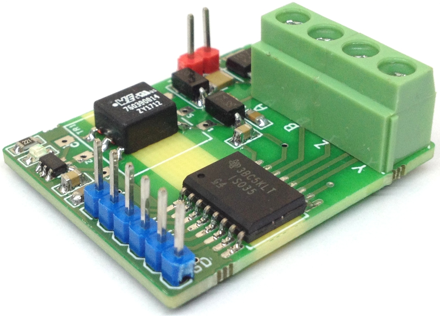
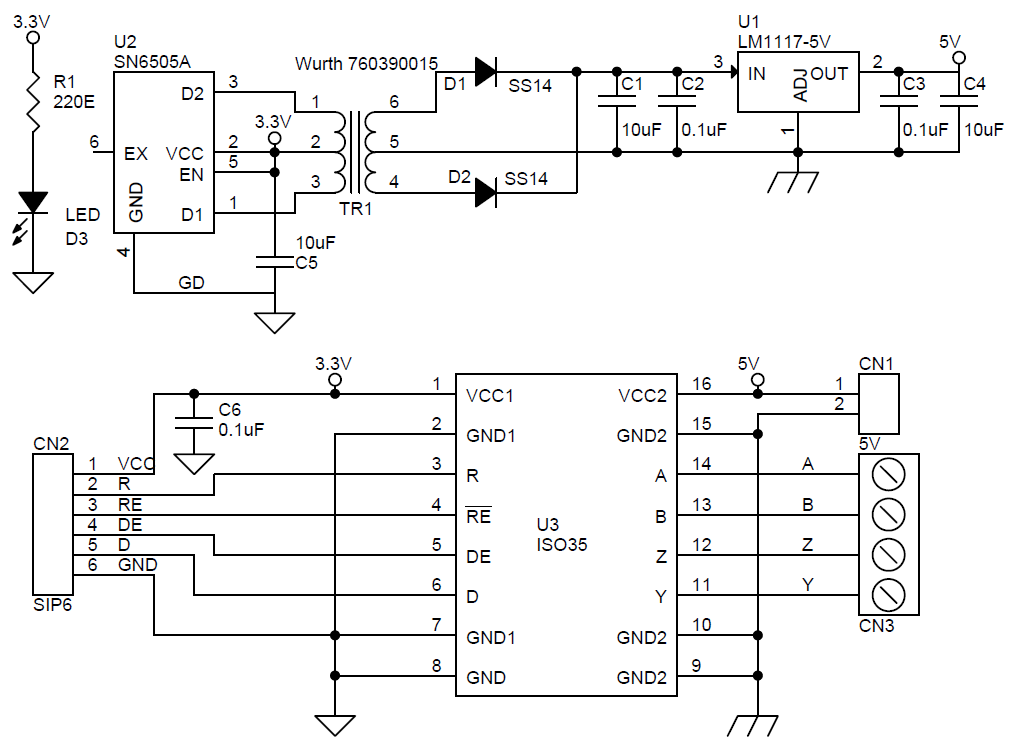
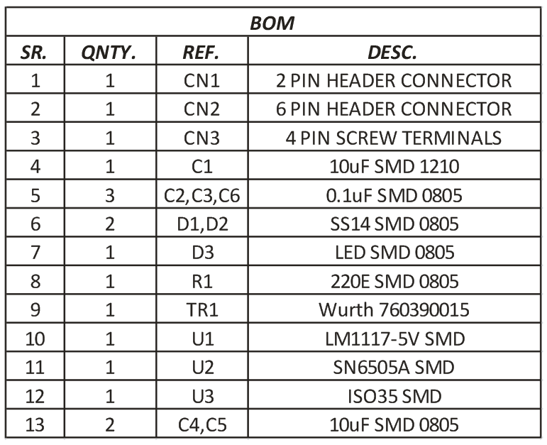
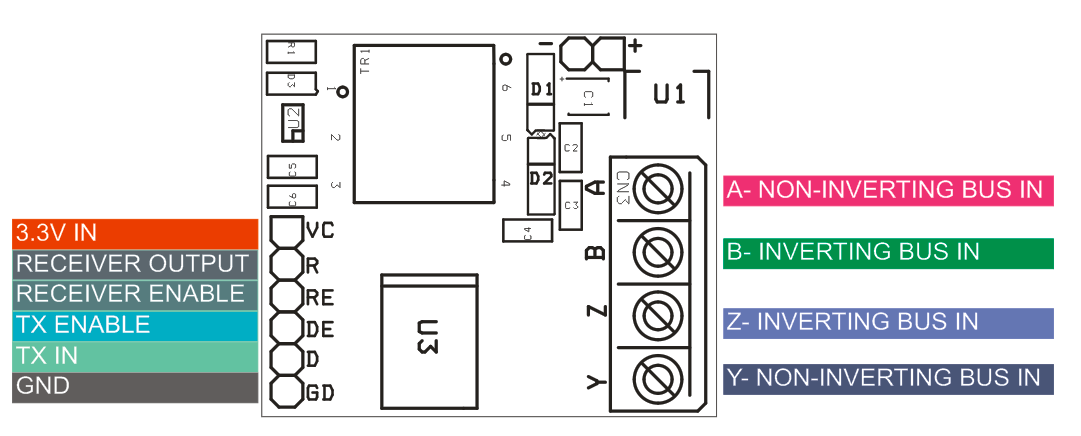
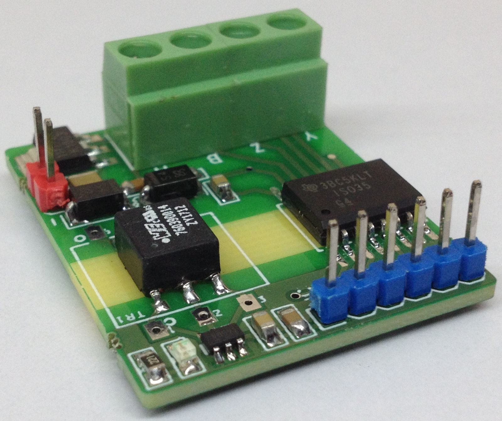
This module is an isolated full-duplex differential line driver and receiver for TIA/EIA RS485/RS422 applications. The module is ideal for long transmission lines because the ground loop is broken to allow for a much larger common-mode voltage range. The symmetrical barrier of the device is tested to provide isolation of 2500Vrms between bus line Trans-receiver and the logic-level interface. The circuit works with a single supply 3.3V input. SN6505 Chip and Wurth Elekronics 760390015 transformer help to generate 5V DC to power up isolated circuitry. Module has been designed using ISO35 IC which is an isolated full-duplex RS485 trans-receiver, SN6505 IC used to form isolated DC-DC converter to power up the bus side of isolated circuitry of ISO35, LM1117-5V IC regulates the output of DC-DC converter and provides 5V DC. CN2 6 Pin header connector provided to power up the board and micro-controller interface, CN3 for Full-Duplex communication. CN1 is for AUX power 5V DC.
Any cables I/O can be subjected to electrical noise transients that can cause damage to the transceiver and/or nearby sensitive circuitry if they are of sufficient magnitude and duration. This module can significantly increase protection and reduce the risk of damage to an expensive control circuit. The device can be used for applications like security systems, chemical production, factory automation, motor control circuit, networked security stations, HVAC and building automation networks.
When the driver enable pin, DE, is logic high, the differential outputs Y and Z follow the logic states at data input D. A logic high at D causes Y to turn high and Z to turn low. In this case, the differential output voltage defined as VOD = V(Y) – V (Z) is positive. When D is low, the output states reverse, Z turns high, Y becomes low, and VOD is negative. When DE is low, both outputs turn high-impedance. In this condition the logic state at D is irrelevant. The DE pin has an internal pull-down resistor to ground, thus when left open the driver is disabled (high impedance) by default. The D pin has an internal pull up resistor to VCC, thus, when left open while the driver is enabled, output Y turns high and Z turns low.
When the receiver enable pin, RE, is logic low, the receiver is enabled. When the differential input voltage defined as VID = V(A) – V(B) is positive and higher than the positive input threshold, VIT+, the receiver output, R, turns high. When VID is negative and less than the negative and lower than the negative input threshold, VIT– , the receiver output, R, turns low. If VID is between VIT+ and VIT– the output is indeterminate. When RE is logic high or left open, the receiver output is high-impedance and the magnitude and polarity of VID are irrelevant. Internal biasing of the receiver inputs causes the output to go failsafe-high when the transceiver is disconnected from the bus (open-circuit), the bus lines are shorted (short-circuit), or the bus is not actively driven (idle bus).
Features
Single Supply 3.3V
Onboard Isolated DC-DC Converter Provides 5V Output for Bus Side Circuitry
CN2 Header Connector for Micro-Controller Interface
4 Pin Screw Terminal for Full-Duplex Communication
Bürklin Electronics, a distributor specialized in high quality electronic components, announced the availability of the new 1552 family of hand-held enclosures from Hammond Electronics. Initially available in six sizes, the IP54 rated UL94-V0 flame-retardant ABS enclosure features an ergonomic design that fits comfortably into the hand, enabling it to be used for long period in applications such as a machine controller or an electric hoist control.
The end panels are removable for easy modification, and for use with flying cables, an alternative end panel with an integral rubberised cord protector and a strain relief bracket is available. An optional wall mounted holder allows the unit to be stored in a convenient location when not in use. The 1552 can also be used as a desktop enclosure. All the launch sizes are 50mm wide and either 22 or 30mm high, with both heights available in lengths of 70, 110 and 150mm. All sizes are available as standard in black and grey with a satin texture.
A recess for a membrane keyboard or a display is moulded in the top face and PCB standoffs are moulded in the base section. The top is secured to the base with four self-tapping colour-coded screws; snap closures are fitted to the centre of the longer units to prevent bowing.
The new 1552 family of hand-held enclosures by Hammond Electronics are available directly from Bürklin by visiting www.bürklin.com. As part of its wide product portfolio Bürklin is also stocking the 1557 series from Hammond Electronics. Bürklin is offering more than 1.8 million products from over 500 reputable and established OEMs; more than 75,000 of these products are permanently stocked at the company’s warehouse and headquarters in Oberhaching near Munich, Germany.
Flex Power Modules’ converters are first generation direct conversion products
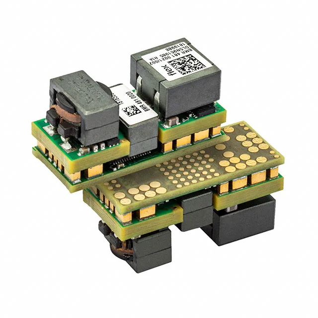
Flex Power Modules’ BMR481 DC/DC converter addresses the growing need for higher energy efficiency levels in datacenters and cloud computing infrastructures. This converter offers an input range of 40 V to 60 V targeting 48 V to 54 V nominal supplies and a programmable 0.5 V to 1.35 V output. The 12 mm x 27.7 mm footprint of the main module provides a maximum output current of 70 A and incorporates a digital interface for monitoring, configuration, and control purposes. This main unit can then be supported by up to five additional ‘satellite’ modules resulting in a total current rating that reaches 420 A.
The single-stage BMR481 provides an ideal alternative to the conventional two-stage intermediate bus converter (IBC) and point-of-load (POL) architecture which requires an extra conversion step, taking up more space and impacts operational performance. This groundbreaking direct conversion module presents engineers with a more streamlined and economical solution. The converter can achieve up to 92% efficiency from a 1 V output at 53 VIN which is 2% to 3% higher than what the equivalent IBC-based deployment can deliver. The BMR481 reduces board area by up to 50%. MTBF is more than 8.7 Mhrs for the main module.
Optimized efficiency is achieved by automatic enabling and disabling of phases/satellite modules depending on the required load, along with dynamic voltage adjustment to provide optimum supply rails to the connected ICs. Output ripple and noise is an extremely low 1 mVp-p (typical) due to the zero voltage/zero current switching employed. Load and line regulation are typically kept at 1 mV. At 53 V input and 0.5 V output, the full 70 A output current is available from the main module to over +75°C ambient temperature with 0.5 m/s airflow and over +90°C with 2 m/s airflow. Full digital control is implemented with a PMBus v1.3 interface compliant with PMBus or AVS/SVID. Isolation is rated at 1,500 VDC (functional).
Features
48 V-to-load direct conversion technology addresses demands of data centers
Enables more compact, higher-efficiency, and cost-effective power system implementations
Researchers at Northern Illinois University and the U.S. Department of Energy’s (DOE) National Renewable Energy Laboratory (NREL) in Golden, Colorado, reported in the journal Nature on a potential breakthrough in the development of hybrid perovskite solar cells.
Considered rising stars in the field of solar energy, perovskite solar cells convert light into electricity. They’re potentially cheaper and simpler to produce than traditional silicon-based solar cells and, on a small scale in laboratory settings at least, have demonstrated comparable efficiency levels. But key challenges remain before they can become a competitive commercial technology.
One major challenge is the use of lead. Most top-performing hybrid perovskite solar cells contain water-dissolvable lead, raising concerns over potential leakage from damaged cells.
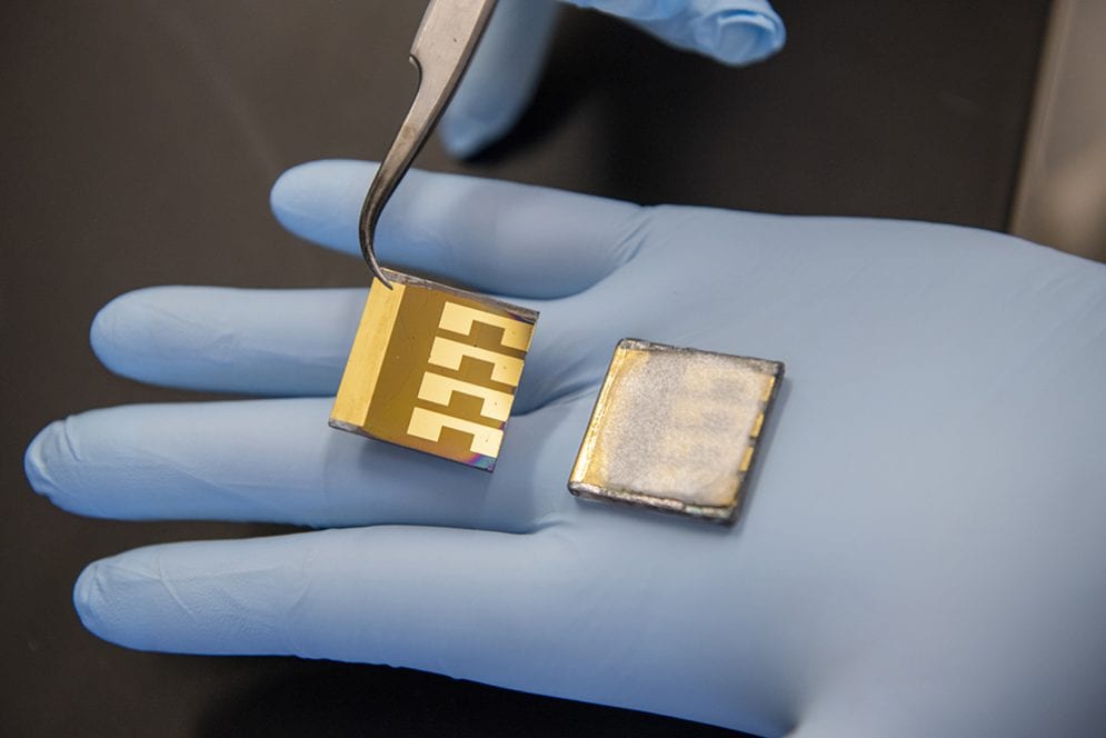
Led by Tao Xu of NIU and Kai Zhu of NREL, a team of scientists has developed a technique to sequester the lead used to make perovskite solar cells and minimize potential toxic leakage by applying lead-absorbing films to the front and back of the solar cell.
“The lead toxicity issue has been one of the most vexing, last-mile challenges in the perovskite solar cell field,” said Xu, an NIU professor of chemistry. “We think we have a highly promising remedy to this problem—and it could be a game-changer.
“In the event of a damaged cell, our device captures the great majority of the lead, preventing it from leaching into groundwater and soils. The films that we use are insoluble in water.”
Under conditions of severe solar cell damage in a lab setting, the lead-absorbing films sequestered 96% of lead leakage, the scientists said. Their experiments further indicate the lead-absorbing layers do not negatively impact cell performance or long-term operation stability.
Perovskite solar cells are so named because they use a class of crystal structures similar to that found in the mineral known as perovskite. The perovskite-structured compound within these solar cells is most commonly a hybrid organic-inorganic lead halide-based material.
Scientists began to study these crystal structures for use in solar cells only about a decade ago and have rapidly increased their solar energy conversion efficiency. Whereas traditional silicon solar cells are produced with precise processes using high temperatures, perovskites can be made using room-temperature chemical solutions.
The newly developed “on-device sequestration approach” can be readily incorporated with current perovskite solar cells configurations, Xu said.
A transparent lead-absorbing film is applied to a conducting glass on the front of the solar cell. The sequestration film contains strong lead-binding phosphonic acid groups but does not hinder cell capture of light. A less expensive polymer film blended with lead-chelating agents is used on the back metal electrode, which has no need for transparency.
“The materials are off-the-shelf, but they were never used for this purpose,” Xu said. “Light must enter the cell to be absorbed by the perovskite layer, and the front-side film actually acts as an anti-reflection agent, improving transparency just a bit.”
Tests for lead leakage included hammering and shattering the front-side glass of 2.5-x-2.5 cm cells, and scratching the backside of the solar cells with a razor blade, before submerging them into water. The films can absorb the vast majority of the lead in severely damaged cells due to water ingress.
“It is worth noting that the demonstrated lead-sequestration approach is also applicable to other perovskite-based technologies such as solid-state lighting, display and sensor applications,” said Zhu, a senior scientist at NREL.
The scientists have applied for a patent for their lead-absorbing films. Other authors on the research study include NIU graduate student Xun Li; Haiying He of Valparaiso University; and Fei Zhang and Joseph Berry of the NREL.
The research was supported by the National Science Foundation and the DOE Solar Energy Technologies Office. The Solar Energy Technologies Office also is providing funding assistance for further development of the lead-sequestration films for hybrid perovskite solar cells.
Xsens MTi-7 Global Navigation Satellite System (GNSS)/Inertial Navigation System (INS) module is a miniature motion tracking module with multiple GNSS receiver support. This module uses advanced sensor fusion algorithms. The MTi-7 GNSS/INS module features a miniature SMD form factor (12.1mm x 12.1mm) and consumes low power. This module is ideal for upcoming technologies including drones, Unmanned Aerial Vehicles (UAVs), smart farming, unmanned control, Internet of (Moving) Things, and robotics.
Features
Industry standard Arduino compatible development kit
High-performance orientation, velocity, and positioning using advanced sensor fusion algorithms
Best-in-class hardware and firmware using same form facto
Uniform software/hardware interface over product lifetime (no end of life)
Printed circuit boards are an important part of electronic products and the ability to get them fabricated in time and at good quality and price, is key to ensuring the product stays on schedule with the time to market plans. The process of getting them done on time, and at the right quality, however, requires a PCB manufacturer with the tools, experience, and support required to deliver as specified. This requirement and the possible impact of failure makes the process of selecting a PCB manufacturing partner a very important and difficult task as there are tonnes of PCB manufacturing companies (including resellers posing as manufacturers) out there and the process of verifying them, can be tedious. To help with this, we review PCB manufacturers from time to time, and today, we will review one of the most formidable names in the PCB manufacturing Industry: PCBWay. We will cover their process, capacity, offerings/packages and every other thing we feel you may need to make decisions about their services.
Located at the heart of the World’s manufacturing capital; Shenzhen, PCBWay has been delivering high-quality complex PCBs using state of the art machines and equipment since its establishment over a decade ago. They have served as a reliable PCB Manufacturing partner for several small or large run projects across diverse sectors, from IoT and Smart devices to medical, Industrial and Open source/DIY communities.
Running one of the most equipped factories in the world, PCBWay makes different types of PCBs ranging from the regular FR4 PCBs to flexible PCBs, SMD stencils, and more advanced, high precision PCBs. They have the capacity to make up to 14 layers PCB (depending on the type of PCB) with different materials from FR4 to Aluminum. More information on their PCB capabilities and equipment specifications can be found on their service description page.
Being a domain leader who understands electronics manufacturing and the headaches involved, PCBWay also runs an In-house PCB Assembly service (PCBA), which ensures the project can be completed under one roof with fewer worries. The PCBA service specializes in prototyping and small-volume production, making them the ideal partner for the R&D stage of product development. The PCBA service also helps eliminate supply chain worries as PCBWay maintains a relationship with suppliers across the world, through which they get access to all types of components including the “hard-to-find” components. More information on the PCB Assembly service is available here.
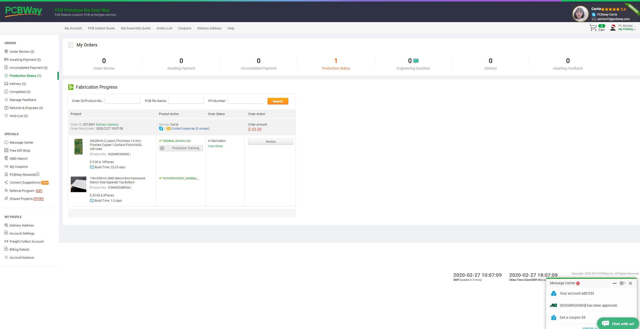
For placing orders, PCBWay uses a transparent, process-oriented, and easy to follow online ordering platform that is structured in such a way that the customer can track the stage of their PCB manufacturing at every point in time. The process starts with a seamless and fast, Instant quote generator through which users can select the type of PCB they want to make, and upload PCB files, in either Gerber, .pcb, .pcbdoc or .cam formats. Once you submit your files they become available in the “Under Review” tab where a human checks the files and provides a quote.
PCBway – Files submitted for Review
The files are reviewed in a timely manner by PCBWay technicians and an instant quote is generated. PCBWay is quite competitive with pricing and probably offers more value for money compared with most other players in the PCB and PCBA industry. After the quotation is done and payment is received, the design moves to “Production Status” and then the fabricating process is started. When fabrication is done the order is shipped to the customer without any further delay.
PCBway – Files approved and being manufactured
One of the best things about PCBWay, which is particularly beneficial to projects in the R&D stage, is their ability to maintain the shortest possible lead-time. In certain cases depending on location and shipping bottlenecks, customers can receive their boards just 24 hours after ordering.
PCBway – Productions steps
PCB Test Order
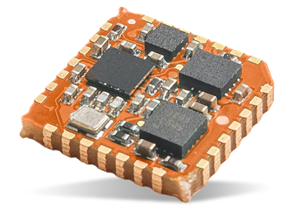
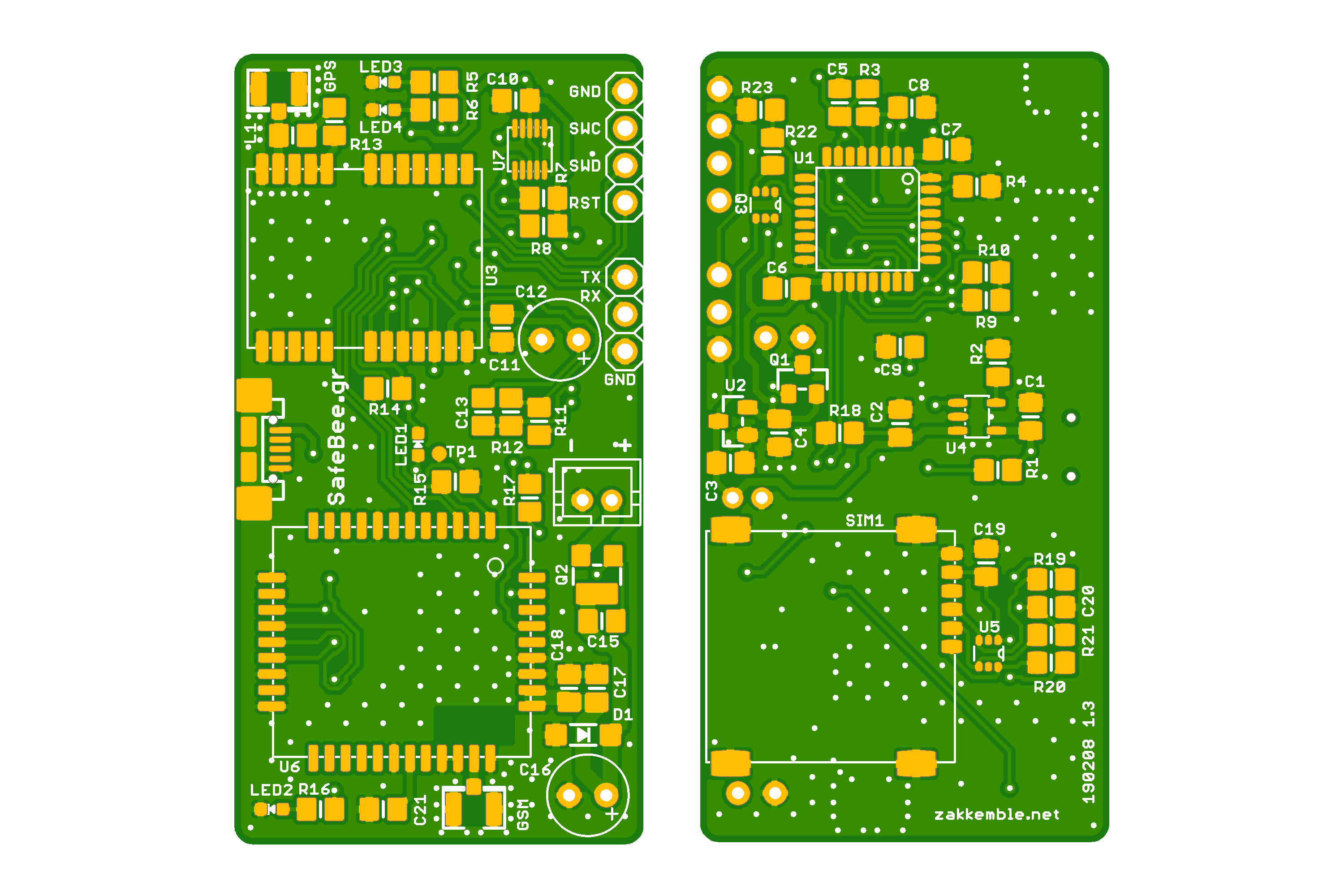
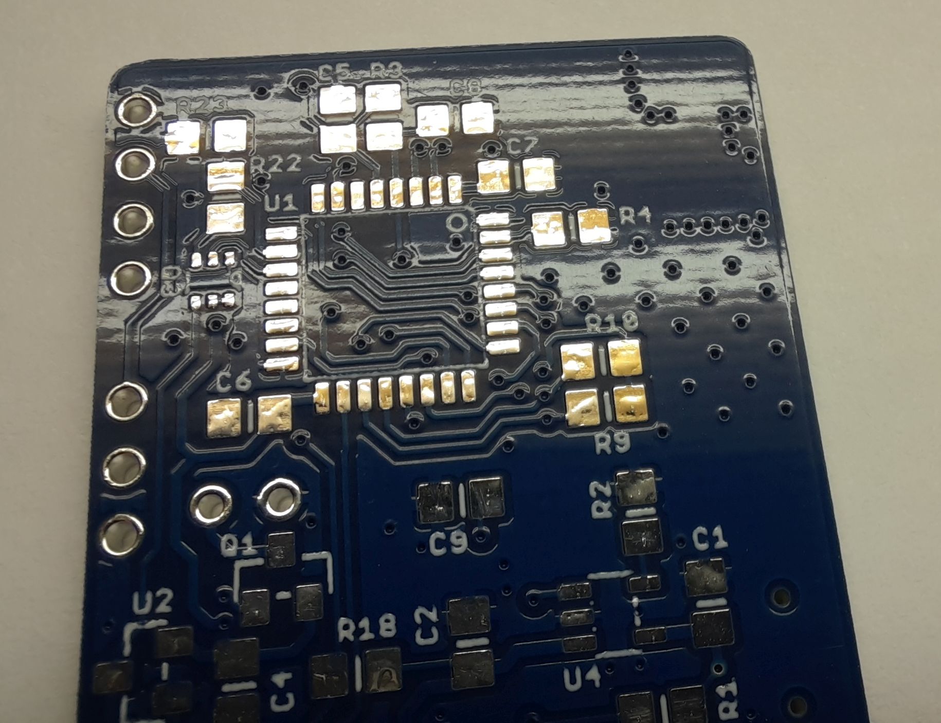
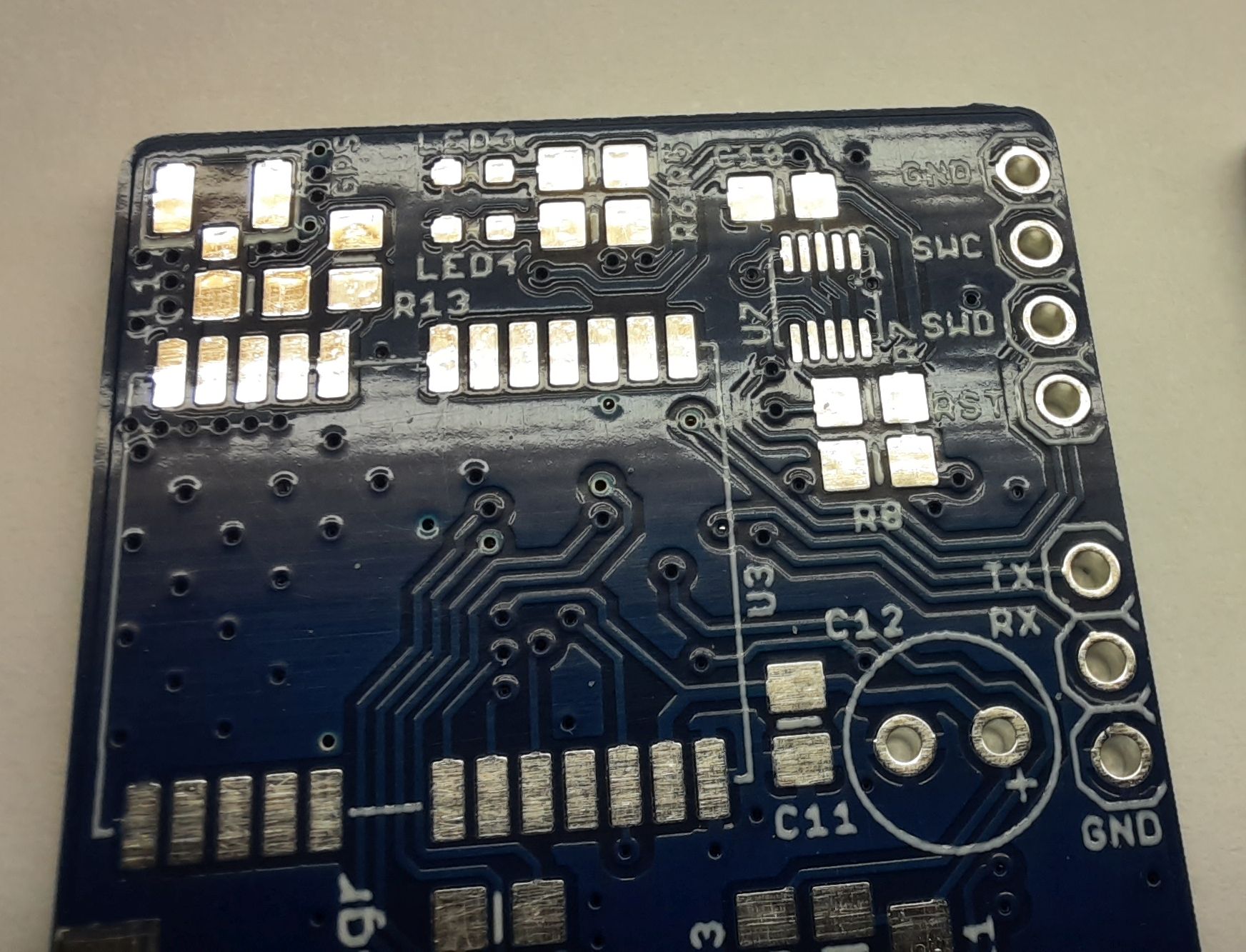
To verify their manufacturing capabilities and quality, we send out our own Gerber files of one of our projects. The board submitted was a 2-layer one, measuring 54 x 28mm. For 10x PCBs and 2x solder stencils (top and bottom) the quote was 25 USD + 28 USD DHL Worldwide shipping. So the total amount we paid was $53. Production time was stated at 22-23 days (this is due to the Coronavirus issue, as the factory was working with limited personnel) for the PCB and 1-2 days for the stencils. The actual production of PCBs was less and took ~6 days from start to finish.
PCBway – the PCB submitted for test production
Unboxing Video
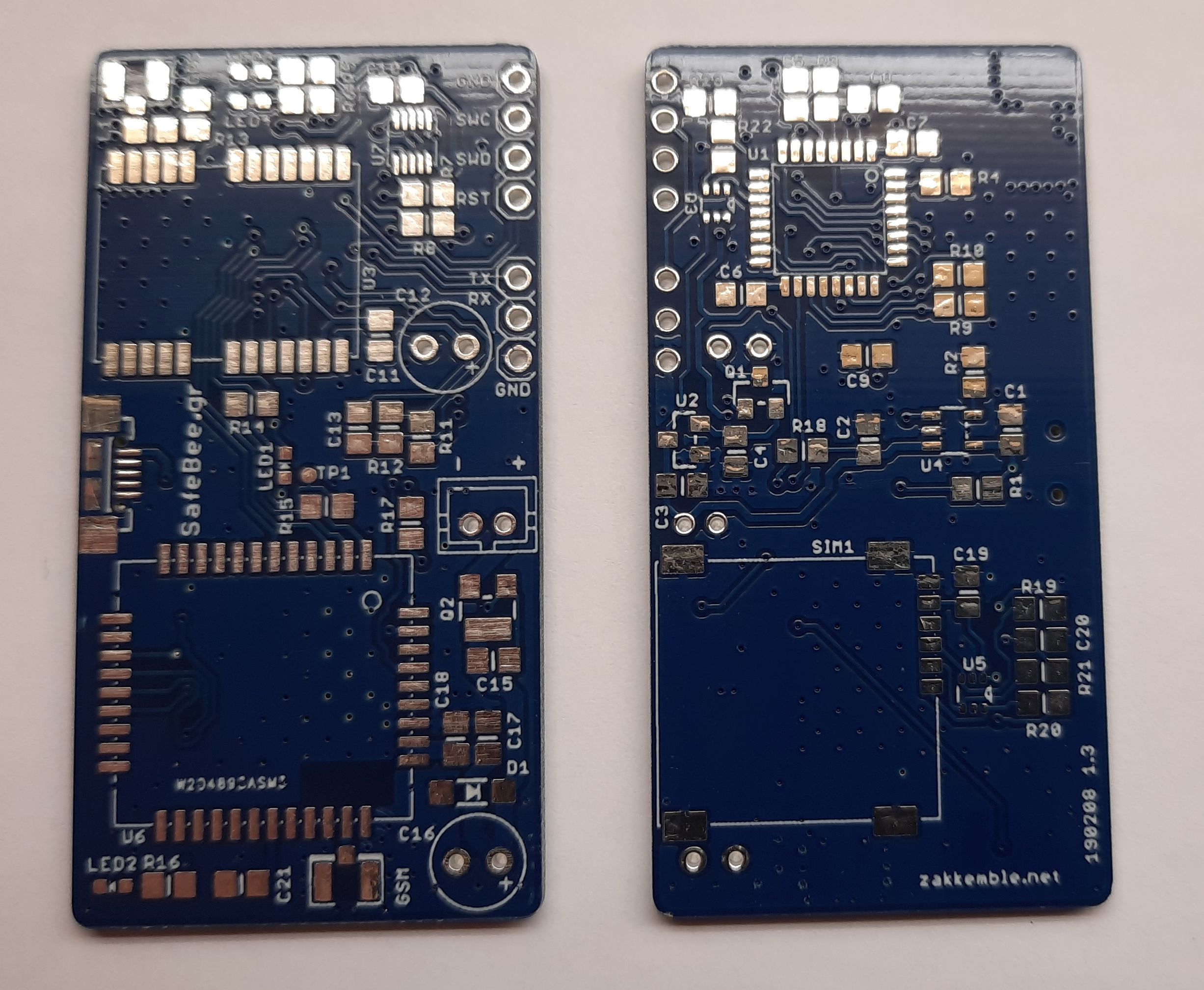
The estimated delivery time for this order was 3-5 days and this was close to real waiting time. The PCB arrived and looked like the following photos.
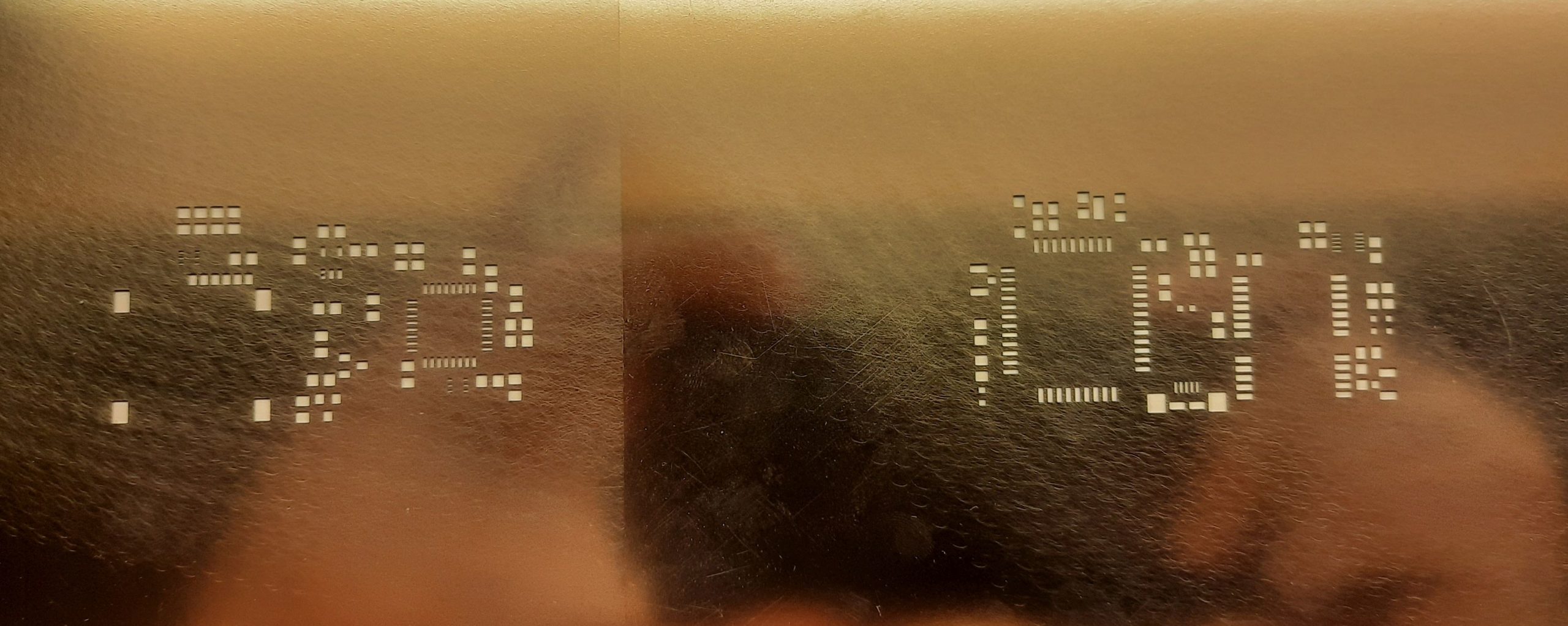
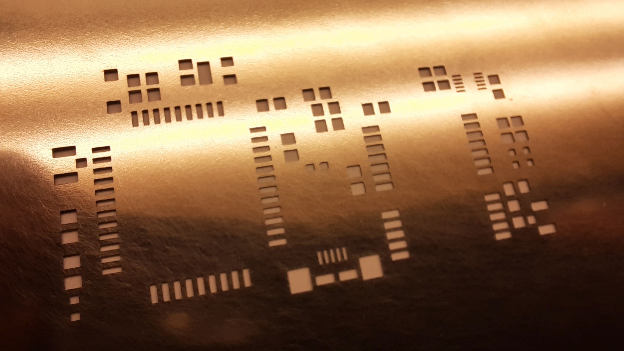
PCBway PCBs arrivedCloseup of bottom layerCloseup of top layerTop and Bottom SMT stencilsCloseup of SMT stencil
We can see from the photos above that the quality is good and we can understand this from the fine pitch components. Silkscreen seems almost sharp and surface finish is what we could expect from HASL. The same applies to stencil quality. The openings are sharp and could work as it should be.
Conclusion
In conclusion, from personal interactions with PCBWay, one consistent factor in all services they offer is a deep thoughtfulness and consideration for the customer. The customer support staffs who are assigned to your projects take the project seriously and work to ensure your deadlines and the quality of the PCB you require are met. This is a trait every designer, engineer or innovator should look out for when choosing a PCB Manufacturer for any project. In terms of quality, the outcome was satisfactory and it meets the demands of most users, professionals, and makers. Delivery and production time was reasonable and one point we can comment on is the price tag. It’s may not be the cheapest manufacturer out there but it will for sure meet your expectations without any surprises.
Mobile devices are continuing to get even flatter in the connected world of today and of tomorrow.
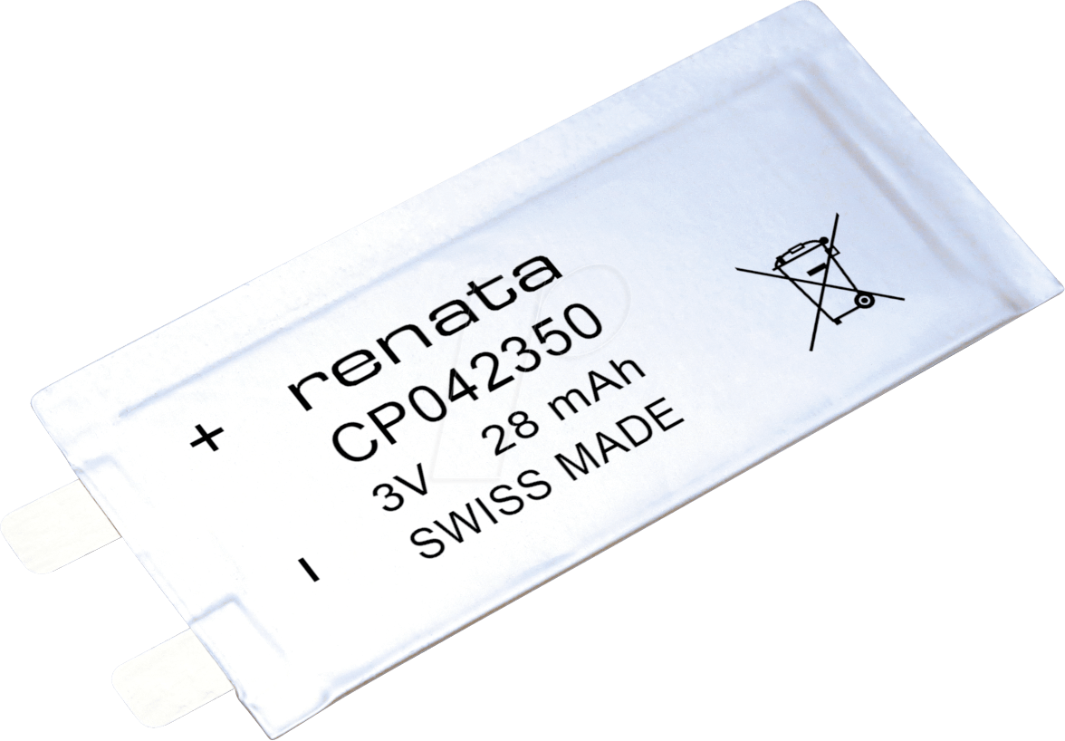
Wearables have become an indispensable part of everyday life and their steady growth is far from getting to an end. Small but powerful: reliable and high-quality batteries that keep pace with the continuous miniaturization are indispensable nowadays. Renata is meeting the growing demands by introducing the right source of energy with the newly developed lithium thin-film battery CP042350.
The ultra-thin 3V battery is ideal for the use in flatter electronic devices since the thickness of 0.42mm is much less than those of conventional primary lithium batteries. The CP042350 is flexible and has successfully passed a 1000 times bending test with a bending radius of 25mm. With a capacity of 28mAh and an average weight of 0.86g, this next-generation battery can be used in a wide range of industrial, medical and consumer devices.
In this tutorial, we present one of the most fundamental and important sets of laws for electrical circuits. These laws have taken the name and been established by the German physician Gustav Kirchoff in 1845.
Like for many physical laws, Kirchoff’s circuits laws (KCL) are relatively easy to understand and emerge from the observation of conservation of energy, which is probably one of the oldest and most fundamental principles in physics.
Nevertheless, KCL might be simple and accessible to understand, they remain a fundamental tool to master for the circuit’s analysis and are still nowadays widely used.
KCL consists of two different laws relative to the physical values that define the energy in an electrical circuit: the current and voltage. In the following, we separately present in two sections, Kirchoff’s current and voltage laws.
Prior to these sections, it is worth presenting in the first section the framework in which KCL laws are used and many definitions associated with this principle.
The third section shows an example of how to apply KCL to a real circuit and solve a problem with unknown parameters.
Finally, the last section presents briefly the limits of KCL for some particular cases.
Framework and definitions
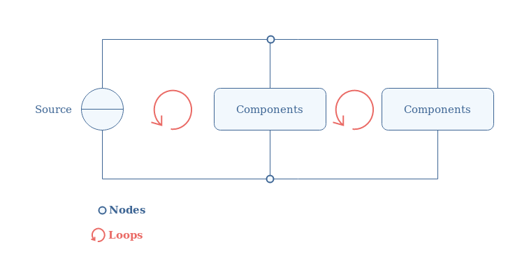
The framework to apply Kirchoff’s laws is electrical circuits, which consist of a power source or generator with both poles connected with the intermediate of components in a closed-loop configuration. Electrical circuits are drawn according to the lumped-element model, which assumes the components to be ideals, and the associated representation is shown in Figure 1 below:
fig 1: Lumped-element model of an electrical circuit
We can give some specific details concerning the topology of the circuits. The straight lines are ideal connections/wires between the different elements of the circuits, which means that they present no resistive or reactive behavior, hence there are no power loss or phase-shift phenomena.
The source provides the circuit with power, which consists of voltage and current signals (either DC or AC). The components are passive, they consist of associations of resistor, capacitor, and inductor. They can either be connected in parallel, such as in Figure 1, or in series. Active components such as amplifiers are not considered in this tutorial since an external source of power is associated with them. A group of components connected at both terminals with wires is called a branch.
Two important topological definitions are important in order to fully understand Kirchoff’s laws later on: the nodes and loops. Nodes represent the junctions between branches, and they are highlighted in Figure 1 by blue circles. The loops are highlighted by red circle arrows in the previous Figure, and it represents a closed path of branches.
Kirchoff current law
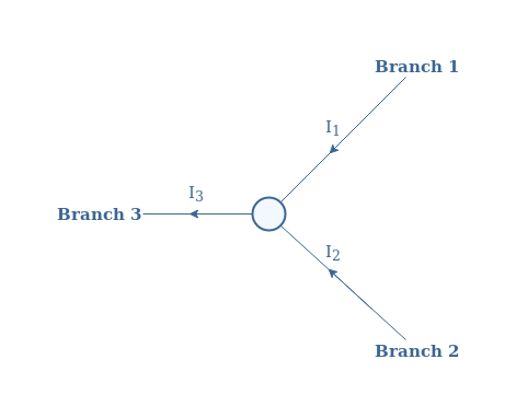
The current law is also known as nodal or junction law and states that the algebraic sum of the currents meeting at a node is equal to zero. A simple example can be illustrated with a node connecting three branches:
fig 2: Node junction of three branches
The law states therefore that the sum of the currents entering the node is equal to the current(s) exiting the junction. In our example, this sentence mathematically translates to I1+I2=I3or I1+I2-I3=0, the current I3 is negative because it is exiting the node.
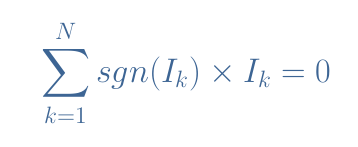
In the general case, a nodal junction of N branches which currents are labeled I1, I2,…, IN satisfies the following Equation 1:
eq 1: Kirchoff’s current law
The sign function sgn is equal to +1 if the current Ik enters the node or -1 if it exists it.
The nodal law is directly written from the observation that the charge in a closed system is invariant. This assumption is also known as the charge conservation principle.
In physics, a principle is an observation that no experience has invalidated but has not been demonstrated, it is the equivalent of postulates in mathematics.
Kirchoff voltage law
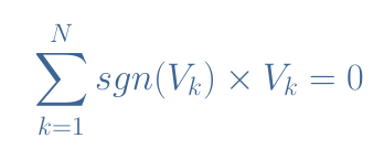
The voltage law is also known as the loop rule, it is very similar to the nodal rule but applies to loops instead of the nodes. This second law states that the algebraic sum of voltages in a circuit loop is equal to zero. A simple example can be illustrated with a DC source powering a series RC filter:
fig 3: Loop with three different voltages
The sign of the voltages is determined with the direction of the arrows, usually, the source is considered positive so that the clockwise arrows are positive and the counterclockwise are negative. The Kirchoff voltage law states therefore that VS=VR+VC or VS-VR-VC=0.
For a loop with N generation and drop of voltages V1, V2,…, VN, Equation 2 is satisfied:
eq 2: Kirchoff’s voltage law
The sign function sgn is equal to +1 when a voltage is generated (the source in our example) or -1 when a drop is observed (with the passive components in Figure 3).
KCL application
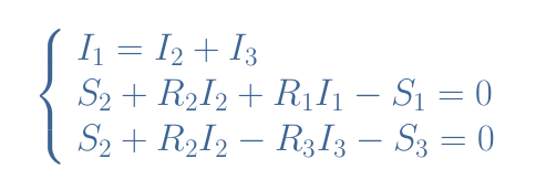
In this section, we show the resolution process of typical problems that can be solved by using KCL. Consider three sources S1, S2 and S3 connected with resistors R1, R2 and R3 in the configuration shown in Figure 4:
fig 4: Example of circuit configuration
The sources are DC and ideal, meaning that they present no internal resistances. We take S1=4 V, S2=3 V, S3= 10 V, and R1=3 Ω, R2=2 Ω, R3=1 Ω.
From Kirchoff’s current law, we can write the following equalities for Nodes 1 and 2:
Node 1: I1=I2+I3
Node 2: I2+I3=I1 which is similar than the equation of Node 1
From Kirchoff’s voltage law, we write the equalities for Loops 1 and 2:
Loop 1: S1=S2+R2×I2+R1×I1
Loop 2: S2+R2×I2=S3+R3×I3
We can differently write these equations to obtain the following system of 3 equations with 3 unknown parameters I1, I2 and I3:
eq 3: KCL linear system of equation
This system can be solved with the elimination method which consists of replacing I1 by I2+I3 in the second line (L2) and eliminate the term I3 by doing the addition R3×L2+R1×L3.
We find directly I2=4.2 A, we can then find I3 by replacing I2 in L3 which gives I3=1.4 A and finally we get I1=I2+I3=5.6 A.
Limits of KCL
In the first section, we have seen the framework where KCL apply but there are also some other more subtle conditions that a circuit must respect. We briefly highlight in this section these further conditions for KCL to be valid.
The first condition is known as the quasistatic approximation and consists to say that the propagation time of the signal must be negligible compared to the period of the signal, this gives a condition on the dimensions of the circuit.
For example, consider an AC signal of 200 kHz (T=5 μs), if a receptor is located in the circuit at D=10 cm, the propagation time will be Δt=D/c=0.33 ns with c being the speed of light. In this case, Δt<<T, the quasistatic approximation is valid and the condition to apply KCL is respected.
However, if the receptor is located instead at D=1 km, the propagation time becomes Δt=3.3 μs and the inequality Δt<<T is not respected, therefore the approximation is not valid and KCL cannot be applied to the circuit.
In the quasistatic approximation, any variation of the source is considered to be immediately propagated at any point in the circuit which avoids delayed effects that can invalidate the KCL.
This affirmation can be demonstrated with the Maxwell-Ampere equation in which the variating term can be eliminated when the quasistatic approximation is valid, the Kirchoff’s current law can then be demonstrated by using the Green-Ostrogradski theorem.
Another common condition to give validity to KCL consists to say that the variations of the magnetic flux across the loops of the circuit must be negligible. According to the induction law, variations of the magnetic flux create induced currents in the circuit and therefore induced voltages.
The variation of flux invalidates the loop rule by introducing a new voltage term that is not explained by the components nor the topology of the circuit but from an external source.
Conclusion
The KCL are fundamental laws of electronics that can be applied to electrical circuits constituted with loops and nodes. These topological definitions along with others are presented in the first section of the article that provides the framework in which the KCL are applied.
Kirchoff’s laws consist of a current and a voltage law that reflects the principle of conservation of energy in a circuit.
The current law accounts for the charge conservation, it states that the algebraic sum of currents in a node is equal to zero. The voltage law states that the algebraic sum of voltages in a loop is equal to zero.
It is presented in a further section that the use of both these laws can solve typical electronic problems by solving systems of linear equations.
Finally, we briefly present in the last section that some subtle conditions about the dimensions of the circuit and the existence of an external magnetic flux must be respected in order for the KCL to be valid.
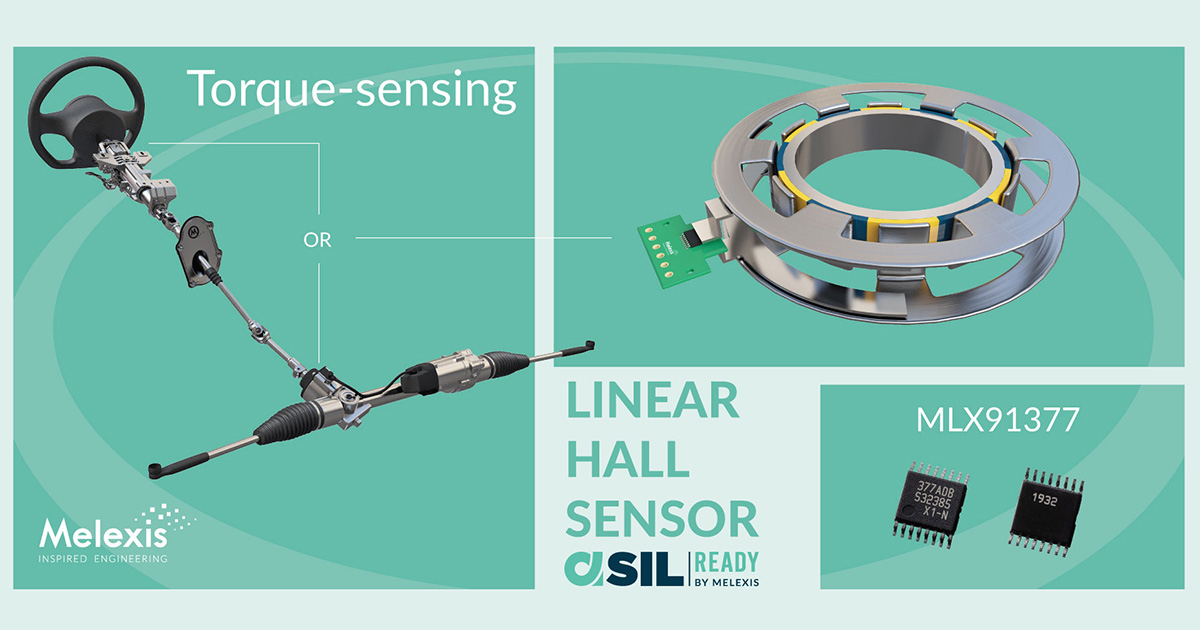
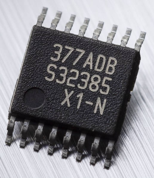
ASIL-ready MLX91377 for steering-torque and general automotive sensing.
Melexis announces the MLX91377 ASIL-ready Hall sensor IC suitable for use in safety-critical automotive systems such as electric power-assisted steering (EPAS).
With an ambient operating temperature up to 160°C and combining high linearity with excellent thermal stability, including low offset and sensitivity drift, the MLX91377 supports accurate, dependable torque sensing in EPAS systems to enable safe control in conventional and autonomous driving.
Developed as a Safety Element Out of Context (SEooC), the MLX91377 complies with the ISO 26262 standard and is qualified to AEC Q-100 Grade 0. Supporting functional safety level ASIL-C in digital (SENT or SPC) mode and ASIL-B in analog mode, the MLX91377 offers a high level of functional safety, per die, and can detect internal failures and enter a safe state to prevent unintended vehicle behavior. The available dual die TSSOP-16 package further expands this by offering two fully redundant dies to enable support for safety critical applications like steering and braking systems.
In addition to functional-safety applications, the MLX91377 satisfies a wide variety of automotive and industrial contactless position-sensing use cases including steering torque sensors, acceleration, brake, or clutch pedal sensors, absolute linear position sensors, float-level sensors, non-contacting potentiometers, small-angle position sensors and small stroke position sensors.
The programmable measurement range and multi-point calibration enhance flexibility for designers, and the variety of output protocols enables one IC to be used in multiple applications reducing requalification efforts and costs. The Short PWM Code (SPC) protocol permits measurements to be taken and transmitted upon detection of a trigger pulse. Thus up to four MLX91377 sensors can be synchronized up to 2 kHz, enabling simultaneous magnetic measurements with deterministic latency to ensure high accuracy. In addition, the low-noise and high refresh rate allow high control-loop speeds enabling systems to deliver fast response times with minimal filtering.
The MLX91377, with its 48-bit programmable identification number, is available in a dual-die fully-redundant TSSOP-16 package.
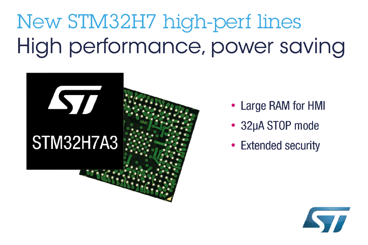
The STM32H7A3/7B3 lines of microcontrollers include an Arm® Cortex®-M7 core (with double-precision floating point unit) running up to 280 MHz.
The STM32H7A3/7B3 MCU lines provides 1 to 2 Mbytes Flash memory, 1.4 Mbytes of SRAM with the following architecture: 192 Kbytes of TCM RAM (including 64 Kbytes of ITCM RAM and 128 Kbytes of DTCM RAM for time-critical routines and data), 1.18 Mbytes of user SRAM, and 4 Kbytes of SRAM in backup domain to keep data in the lowest power modes and 64- to 225-pin packages in BGA and LQFP profiles.
Performance
280 MHz fCPU/, 1414 CoreMark /599 DMIPS executing from Flash memory, with 0-wait states thanks to its L1 cache.
L1 cache (16 Kbytes of I-cache +16 Kbytes of D-cache) boosting execution performance from external memories.
Security
STM32H7B3 MCUs include the following additional security features:
Crypto/hash hardware acceleration
On-the-fly decryption on Octo-SPI external serial flash memory
Secure Firmware Install (SFI) embedded security services to authenticate and protect your software IPs while performing initial programming.
Secure Boot Secure Firmware Update (SBSFU)
Power efficiency
Dual-power domain architecture enables each power domain to be set in low-power mode to optimize power efficiency
Embedded SMPS to scale down the supply voltage. It can also be used to supply external circuitry and can also be combined with the LDO for specific use cases
120 µA/MHz typical @ VDD = 3.3 V and 25 °C in Run mode (peripherals off) and SMPS
32 µA typical in STOP mode (low-power mode)
2.2 µA typical in Standby mode (low-power mode)
0.74 µA typical in VBAT mode with RTC (low-power mode)
Graphics
LCD-TFT controller interface with dual-layer support
Chrom‑ART Accelerator™ boosts graphical content creation while saving core processing power, thus freeing up the MCU for other application needs
Chrom-GRC™ optimizes RAM use
JPEG hardware accelerator for fast JPEG encoding and decoding, off-loading the CPU
Embedded peripherals
Up to 35 communication interfaces including FD-CAN, USB 2.0 high-speed/full-speed, camera interface, Parallel synchronous data input/output slave interface (PSSI)
Easily extendable memory range using the flexible memory controller with a 32-bit parallel interface, or the dual Octo-SPI serial Flash memory interface
Analog: Dual 16-bit ADCs
Multiple 16- and 32-bit timers running at up to 280 MHz