Sine Wave-Based Inverter with SLG47004 AnalogPAK

Author: Pablo E. Leibovich and Alberto I. Leibovich

Introduction

Climate change and its consequences have increased concern about how to replace fossil fuels with cleaner and more sustainable alternatives for electricity generation. Renewable energy sources, such as solar, wind, hydropower, biomass, and geothermal energy, have emerged as real solutions with huge development. They refer not only to large wind or solar farms but also to domestic generation, with small solar panels or wind turbines that replace or reduce the cost of energy from the public electric grids.

However, these sources typically generate DC electricity, while most applications and the electrical grid operate on AC. Inverters bridge this gap by converting DC power into AC power, making renewable energy sources compatible with existing infrastructure.

Similar considerations can be related to automotive applications. Various devices and portable equipment require AC power which may be not available on a trail, campsite, or different locations where the only available electrical power can be received from the car battery. As it is a DC power supply, inverters are mandatory to get the required AC power from the battery.

To implement the power conversion, DC-AC inverters usually apply the Pulse Width Modulation technique. PWM is a widely used technique where switches like Power MOSFETs are controlled with pulses of variable widths, to obtain an automatic control and regulation of AC voltage output (and its frequency), keeping it at the nominal value independent of the output load.

There are several studies and technologies that have been developed to determine how to obtain a better response from the inverter control system. From all these resources, and evaluating the available devices in the market, it can be concluded that inverters that change the output voltage according to the changes in the load and generate a sinusoidal AC voltage waveform are the best alternative to obtain AC power from DC sources without generating electromagnetic compatibility issues, such as switching losses or harmonic generation.

This article describes how to build a sine wave-based inverter useful for automotive and renewable energy applications. The article explains the implemented logic, the SLG47004 AnalogPAK’s configuration and the obtained results of a highly integrated inverter. The internal design was implemented in the Go Configure Software Hub. The complete design file can be found here: Sine Wave-Based Inverter.gp.

Design Description

To obtain DC-AC conversion, PWM-based inverters regulate the output voltage by changing the width of the pulses generated at a comparatively high frequency. Therefore, the output voltage depends on the switching frequency and pulse width, which varies according to the value of the load connected to the output. Several methods of generating pulse width modulation have been studied, being sinusoidal pulse width modulation (SPWM) the widely used in power electronics as the modulation method for PWM inverters.

As mentioned before, a single-phase design requires switching transistors, MOSFETS or IGBTs on each arm of an H-bridge with antiparallel freewheeling diodes to discharge current when the switch is turned off, as it is shown in Figure 1.

Figure 1: Basic H-bridge Circuit

Q1-Q4 signals are the SPWM outputs of the inverter controller.

An inverter controller can be implemented by considering the block diagram shown in Figure 2.

Figure 2: Inverter Schema

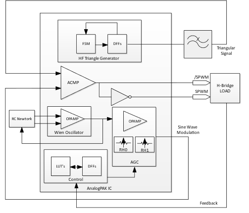
A high-frequency triangular waveform, generally in several kHz, is necessary to generate the SPWM signals. This task is implemented with finite state machines (FSM)/Counters, D-type Flip Flops, and a low pass external filter. It is referenced as HF Triangle Generator in the previous diagram and is based on the AN-CM-265 Programmable Limits PWM application note. The generator output is a PWM signal with triangular variation of duty cycle, which is then filtered by a low pass filter to obtain a triangular shape.

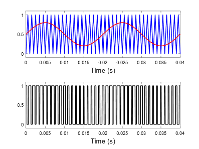
This triangular waveform is compared to a low voltage 50 or 60 Hz sine waveform with the Analog Comparators of the AnalogPAK. With this comparison, the sinusoidal modulation of the PWM is implemented. The modulation scheme, and the obtained signal, are shown in Figure 3.

Finally, an inverter gate is used to generate the complementary signals for the SPWM outputs (S1 to S4 in Figure 1). The output of the H-Bridge contains an LC-filter so the high-frequency component of the SPWM is filtered and, finally, the sinusoidal waveform of 50 or 60 Hz is applied to the load.

Figure 3. Sine Based PWM Modulation and Output Signal

To obtain better results, the frequency ratio between the triangular and the sinusoidal waveforms must be an integer N = fC/fS, where fC is the carrier frequency (the triangular waveform) and fS is the modulation frequency (the sine waveform). With this condition, the number of voltage pulses per half-cycle results in N/2.

The amplitude of the output signal can be controlled by changing the amplitude low-frequency sine waveform. If a short mathematical analysis is performed, a modulation index m can be defined as the ratio between the amplitude of the low frequency sine wave (VS) and the high frequency triangular wave (VC):

For regulation range, m must be equal or less than 1.0. If the previous condition is considered, the output voltage of the H-bridge controlled by SPWM results:

Where VDC is the input DC voltage to the inverter.

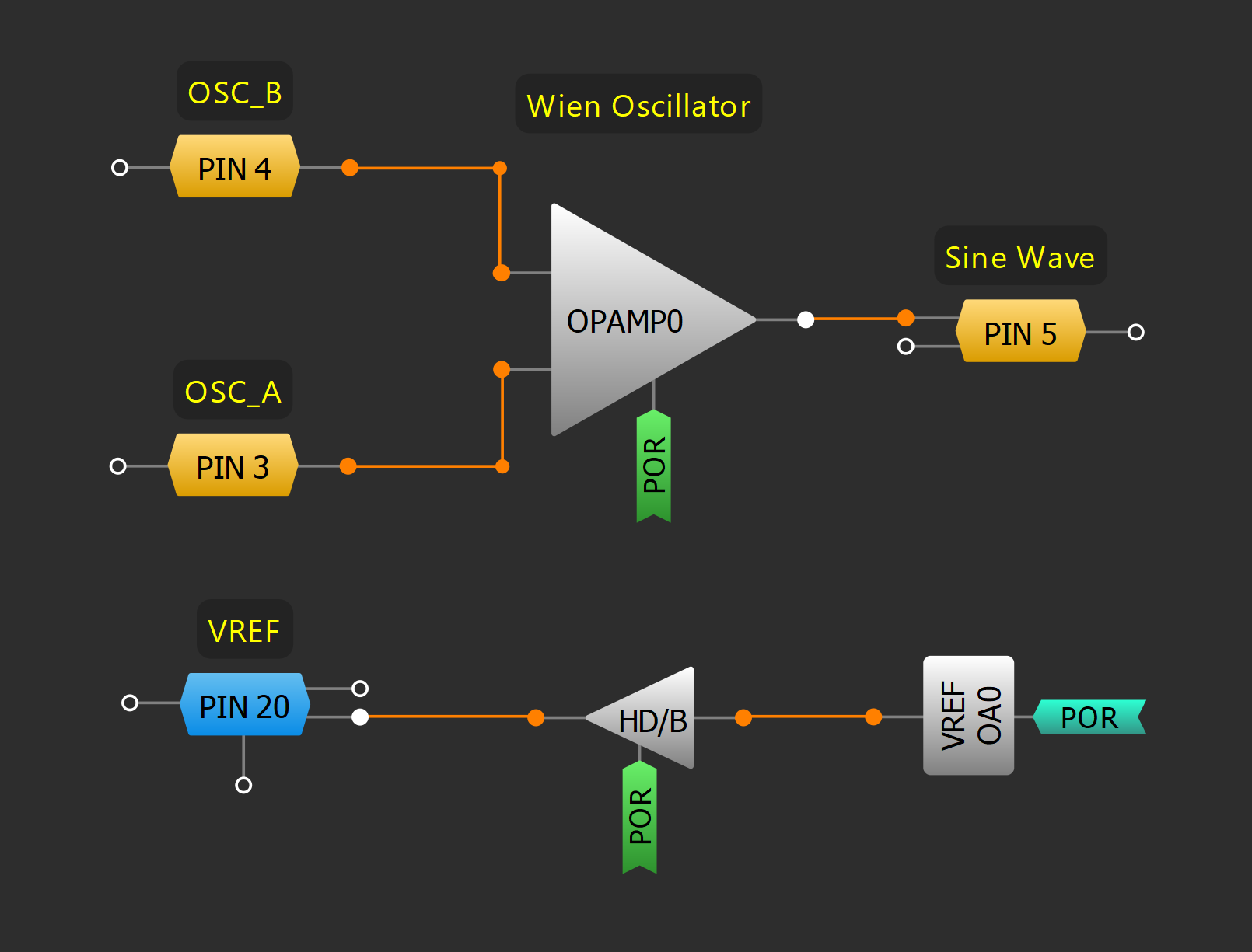
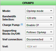
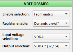
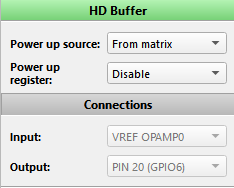
In this article, the fixed frequency sine waveform is generated with a Wien oscillator based on the AnalogPAK’s internal OPAMP and a RC external network to set the oscillation frequency. In Figure 4, the schematic circuit can be seen.

Figure 4: Wien Oscillator

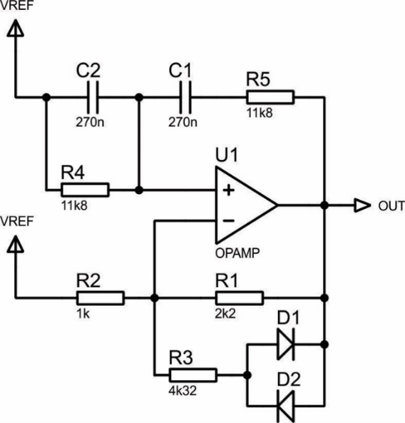
As one of the main issues of the Wien oscillator is its frequency instability, the OPAMP’s gain must be exactly 2 to start oscillating without distorting the sine wave output signal. To do so, precision resistors should be used. Also, as not only the temperature changes but also the voltage fluctuations, and the OPAMP’s imperfections can affect the output, a soft clipping circuit is included.

The offset of the sine wave is set by the VREF voltage (corresponding to VDD/2), and the amplitude is controlled by an automatic gain control (AGC) implemented with another internal OPAMP and the digital rheostats of the AnalogPAK. The amplitude control is implemented as output feedback, to regulate the output voltage of the inverter. This control is implemented with internal Analog Comparators that vary the rheostat counter depending on the output voltage. The corresponding schematic circuit is shown in Figure 5.

Figure 5: SPWM Regulator

Sine Wave-Based Inverter Implementation

As described earlier, the High Frequency Triangular Waveform generator, is based on the AN-CM-265 Programmable Limits PWM application note, so a high frequency PWM signal with a triangular variation of duty cycle is obtained. The implementation of the generator can be seen in Figure 6.

Figure 6: Triangle Waveform Generator

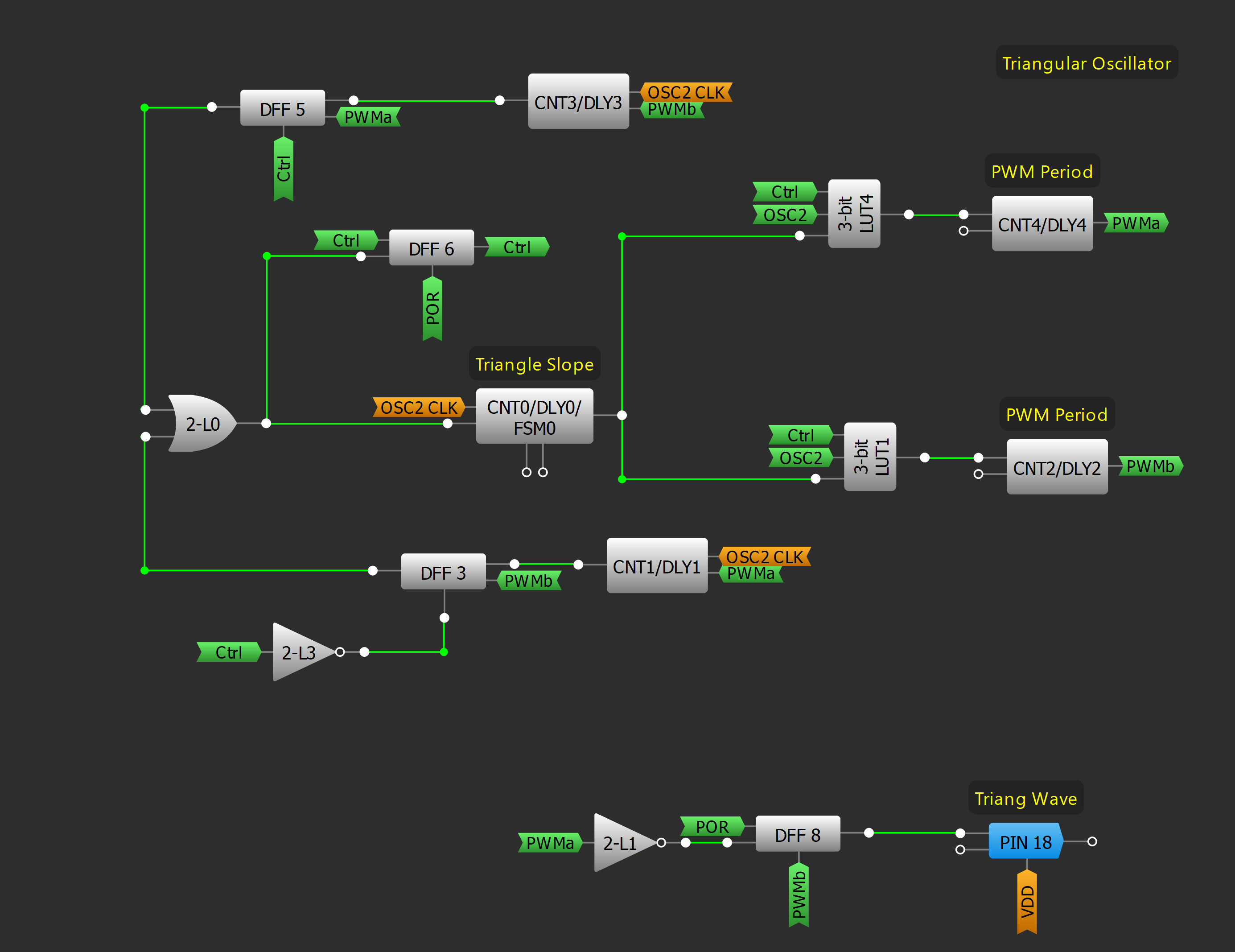
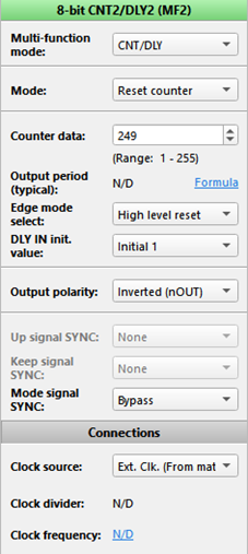
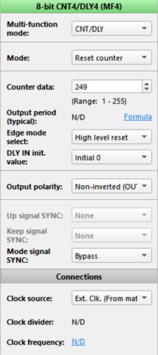
The generator is based on the internal OSC2 25 MHz oscillator, configured for an output frequency of 12.5 MHz. This clock is the time base used for PWM generation with CNT2 and CNT4, which generate the corresponding square waveform with the desired duty cycle. Counter data of both counters is defined to obtain a PWM of 50 KHz. The configuration of both counters can be seen in Figures 7 and 8.

Figure 7: CNT2 Configuration
Figure 8: CNT4 Configuration

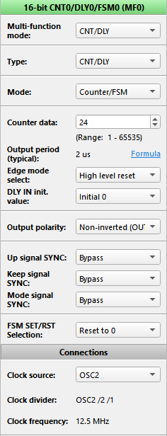
To vary the generated duty cycle, CNT0/DLY0/FSM0 is used to change the relative phase of the previously mentioned counters. The slope of triangular duty cycle variation is configured by setting CNT0 counter data.

With the configuration shown in Figure 9, the triangular waveform has a period of 1 ms (it must be considered the positive ramp and the negative one), so a 1 kHz triangular waveform is obtained.

It is important to mention that in this article, a 50 Hz SPWM inverter is implemented. If desired, it can be modified for 60 Hz or other frequencies by only changing the period of the triangular and sine waveform.

Figure 9: CNT0 Configuration

The high frequency PWM with triangular variation is connected to PIN 18, where the previously mentioned low pass filter is connected. This filter is based on a first-order RC design, with a 1.5 kΩ resistor and a 10 nF capacitor. With these values, the cut-off frequency of the filter results 10.6 KHz.

As described earlier, another oscillator must be implemented. In this case, a sinusoidal oscillator is required to generate the SPWM. Therefore, a Wien-based oscillator is implemented using the OPAMP0 of the AnalogPAK. The reference voltage necessary to generate the sine wave with VDD/2 offset is obtained from the VREF of this operational amplifier and with the HD Buffer. Its block diagram is shown in Figure 10 and the configuration of the mentioned blocks is shown in Figures 11, 12 and 13 respectively.

Figure 10: Wien Oscillator Block Diagram


Figure 11: OPAMP0 Configuration
Figure 12: VREF OA0 Configuration
Figure 13: HD Buffer Configuration

In Section 3, the SPWM principles were described. It was mentioned that the amplitude of the sinusoidal waveform allows the inverter to regulate the voltage output. To do so, the regulator shown in Figure 5 is implemented.

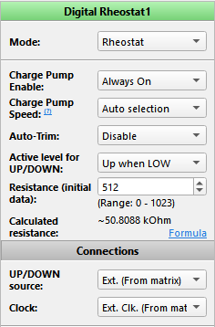
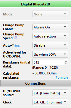
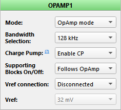
RH0 and RH1 must have the same counter value, that is, the same resistance, to allow the OPAMP1 to amplify the sine wave without distorting its offset. This amplifier has a variable gain (determined by the values of RH0 and RH1), enabling the regulator to amplify or reduce the sine waveform amplitude. This gain change is defined by the output voltage feedback.

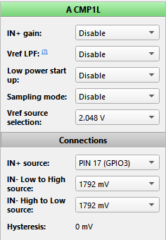
The output voltage feedback is compared to a reference fixed voltage with the analog comparator ACMP1L. If the output is higher than the reference voltage, the OPAMP1 gain goes low and if it is lower, the gain goes high.

This control is made every 31 ms, with a clock signal obtained from OSC0.

The block diagram of the voltage regulator is shown in Figure 14.

Figure 14: SPWM Regulator Block Diagram

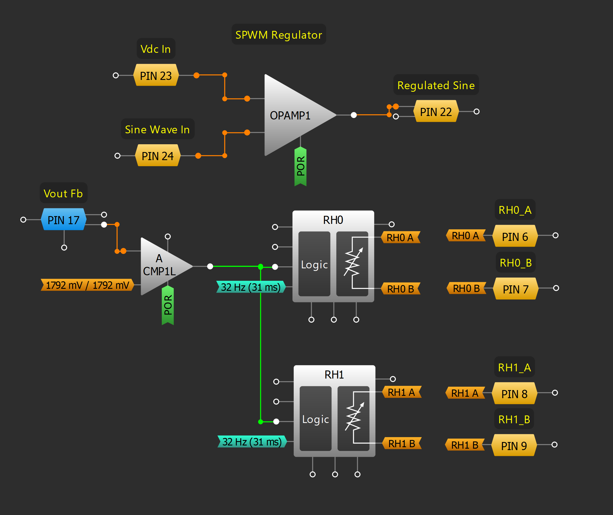
Both RH0 and RH1 are configured as rheostats, with an initial rheostat counter value set to obtain a unitary gain. Their configurations are shown in Figures 15 and 16.

Figure 15: RH1 Configuration
Figure 16: RH0 Configuration

The OPAMP1 and ACMP1L configurations can be seen in Figures 17 and 18, respectively.

Figure 17: OPAMP1 Configuration
Figure 18: ACMP1L Configuration

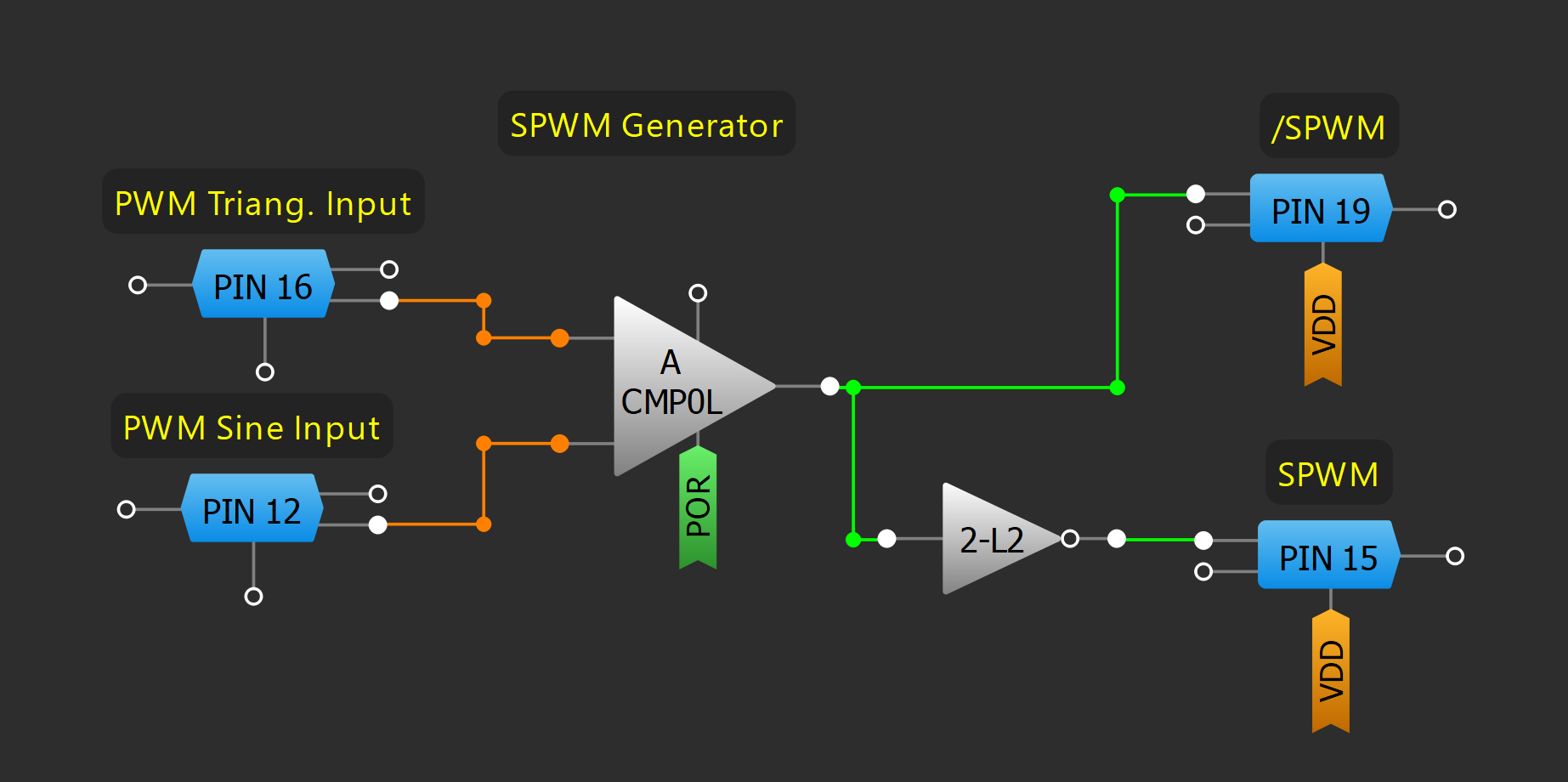
Finally, the SPWM modulator is implemented with ACMP0L and the 2-bit LUT2 is configured as an inverter. It is shown in Figure 19. In Pin 19 and Pin 15, the SPWM output and its inverted version are obtained, ready to control the H-bridge output.

Figure 19: SPWM Generator Block Diagram

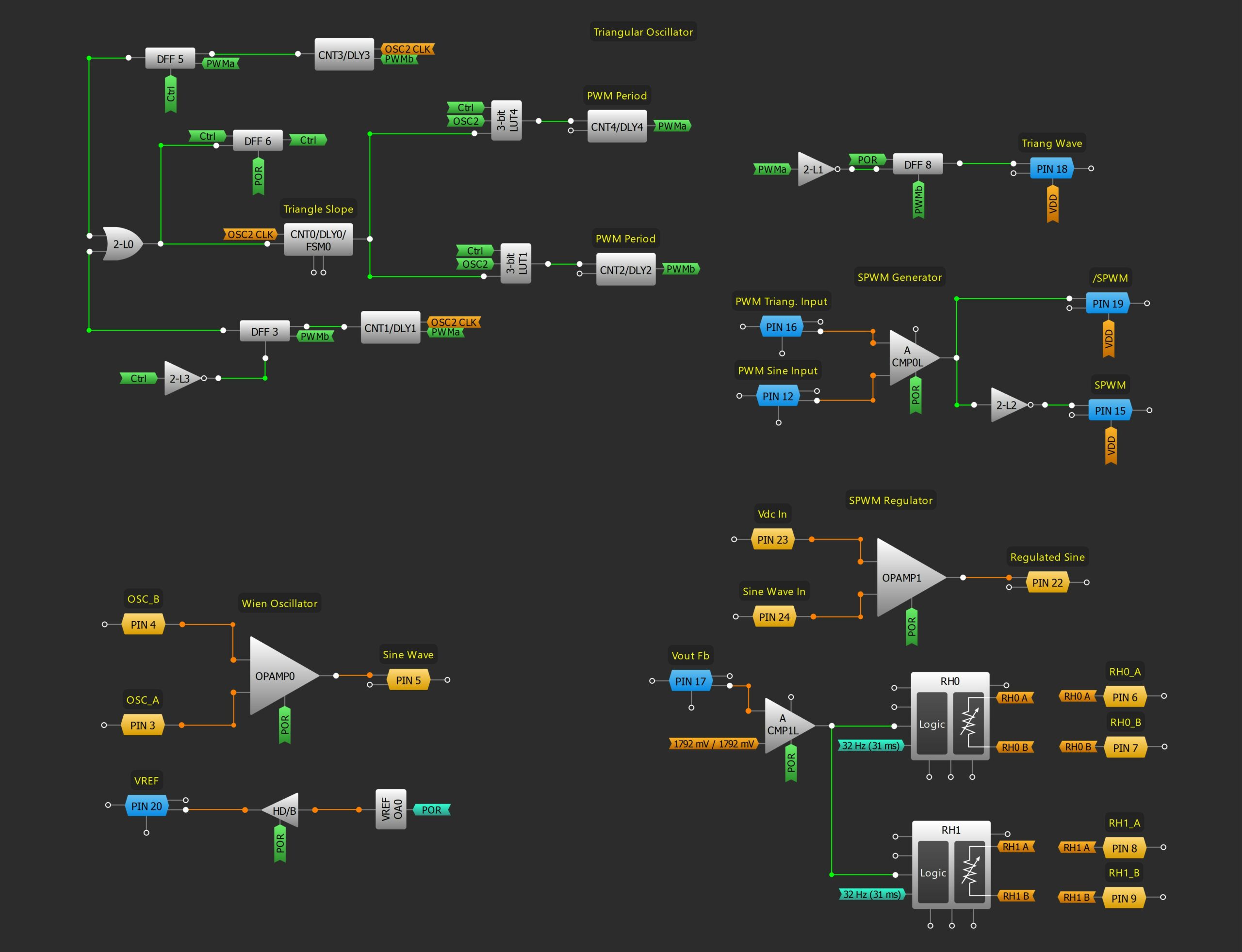
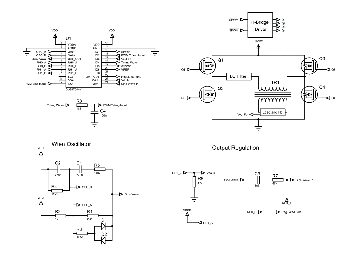
The entire block diagram of the sine wave-based inverter and the schematic circuit are shown in Figure 20 and Figure 21.

Figure 20. Sine Wave-Based Inverter Block Diagram
Figure 21: Sine Wave-Based Inverter Schematic Circuit

Test and Conclusion

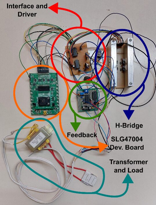
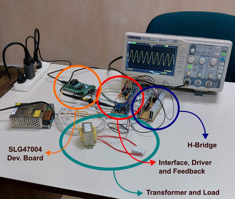
To test the implementation, the entire system was assembled. In Figure 22, different parts of the design that are assembled and interconnected are shown.

This implementation was entirely connected and analyzed with an oscilloscope.

The hardware and measurement tools can be seen in Figure 23.

Figure 23: System Implementation

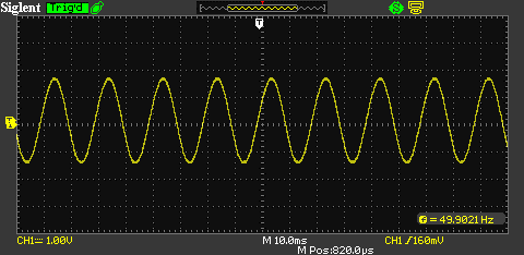
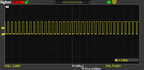
To verify the results, the voltage’s waveform at the load (scaled by a feedback network) and the output signal on Pin 19 of the SLG47004 were measured.

In Figure 24, the feedback of the output voltage (before the rectifier) is shown. It can be seen how the output voltage has a sinusoidal shape as was expected.

Figure 23: System Implementation

In Figure 25, the SPWM output signal at Pin 19 of the SLG47004 is shown. It can be noted the sinusoidal variation of the duty cycle at the PWM output.

Figure 24: Inverter Output Voltage

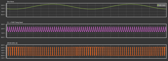
In the same way, different parts of this design were simulated using the software simulation of the Go Configure Software Hub. As this is quite a complex design, and with slow phenomena (20 ms period) if it is compared to simulation period, the first cycles of the design are shown in the simulation results.

The triangular wave oscillator and SPWM were simulated separately from the rest of the design, injecting a simulated sine wave to the sine input of the SPWM generator.

Figure 26 shows the injected sine waveform, the triangular waveform output at the simulated RC filter and the /SPWM Output (Pin 19). It can be seen how the duty cycle of the /SPWM output experiments a sinusoidal variation, as expected.

Figure 25: SPWM Output Signal 1

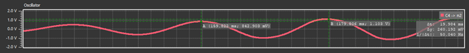
The Wien-based oscillator was also simulated. Its output, with a simulated AC coupling, is shown in Figure 27. As mentioned before, it is important to note that the first cycles are the transient cycles. However, it is useful to show the oscillation with the corresponding frequency (50 Hz).

Figure 26: SPWM Simulation
Figure 27: Oscillator Simulation

An inverter is a key component for renewable energy applications or portable devices that require an AC voltage power supply, and sinusoidal pulse width modulation (SPWM) is one of the most used methods for implementing them.

There are several methods to implement SPWM inverters. One of the simplest and most used methods was represented in this article. It describes each step of SPWM generation and regulation, and how it can be connected to the output. The size of the entire system is smaller than many other implementations and it shows an application where the Renesas’ AnalogPAK can be used as the core of the device.

Grove Vision AI V2 Features Himax WiseEye2 and Arm Ethos-U55 MicroNPU

SeedStudio has recently introduced the “Grove Vision AI V2” An AI-based camera module based on the HiMax WiseEye2 HX6538 dual-core Cortex-M55 AI microcontroller. The module works with an OV5647 camera module, and can be used for AI computer vision applications.

Previously we have covered Tokay Lite, ADLINK AI camera, UnitV2, and many other AI camera modules, feel free to check those out if interested in the topic.

The HiMax WiseEye2 HX6538 is a high-performance, ultra-low power AI microcontroller, featuring an Arm-based Cortex M55 CPU and Ethos U55 NPU, designed for a wide range of AI applications including industrial automation, smart cities, and IoT devices. This chip is designed in a joint effort by Himax Technologies and Seeed Studio, as a result, it now has a 32-fold increase in inference speed and 50-fold improvement in energy efficiency over its predecessor H6537, making it a leading choice for endpoint AI solutions and innovations in vision AI.

Grove Vision AI V2 specifications:

  • Microcontroller: Equipped with the Himax WiseEye2 HX6538 processor, featuring a dual-core Arm Cortex-M55 and an integrated Arm Ethos-U55 microNPU.
  • Processor Frequencies:
    • Arm Cortex-M55 (Big) – Up to 400MHz
    • Arm Cortex-M55 (Little) – Up to 150MHz
    • Arm Ethos-U55 MicroNPU – Up to 400MHz
  • Onboard Peripherals: Includes a PDM Microphone and an SD Card Slot.
  • Interface Options:
    • Camera Interface: Standard CSI for OV5647 camera module.
    • Other Interfaces: IIC, UART, SPI, and USB Type-C.
  • Power Supply Options: Supported through a dual 7-pin connector, USB Type-C, and a Grove Connector.
  • Input Voltage: 5V power input.
  • Internal System Memory:
    • Configurable system memory, up to 2432KB
    • 64KB boot ROM
  • Storage Options:
    • Memory Card Interface supporting up to 1x SD and SDIO host in DS mode at up to 25MHz.
    • Additional 16MB flash storage for firmware.
  • Default UART Speed: Communication rate set at 115200.
  • I2C Interface Compatibility: Compatible with Seeed Studio XIAO and Arduino platforms.
  • Firmware Burning Interface: Via USB Type-C.

Seeed Studio offers resources for Arduino programming, SenseCraft AI model deployment, Home Assistant integration, and advanced Himax SDK guidance, all accessible via their wiki. The Grove Vision AI V2 is ideal for industrial automation, smart cities, transportation, smart agriculture, and battery-powered IoT devices.

The Grove Vision AI Module V2 is available on Seeed Studio for $15.99, which includes only the board. There is also the option to buy the Kit which will cost you $28.88.

LILYGO T-Panel Combines ESP32-S3 and ESP32-H2 with A 4-inch HMI Display

The LILYGO T-Panel is a compact module that works as both a display and a control center for smart devices. It has a 4-inch screen and can connect to WiFi and Bluetooth. It also supports smart home standards like Zigbee, Thread, and Matter. Plus, it has options for adding more features.

Last year, Espressif showed that you can make an IoT Hub with two ESP modules with their ESP Thread Border Router, and this year we found out about the LILYGO T-Panel which is the first product to use this idea, combining two ESP modules in one board as A IoT Hub.

The company mentions the device will support programming with Arduino IDE and PlatformIO-IDE. However, as mentioned in the GitHub repository, the ESP32-H2 model can only be programmed using the Arduino IDE. repository. In the repository, you will also find firmware for ESP32-S3 and ESP32-H2 models, examples for using the main features like the display, RS485, SD card, and WiFi, and the PDF schematics.

After going through the resources you will find that like other LILYGO products, the T-Panel requires users to program software themselves to get started. For that, you can either use Arduino code or firmware from Espressif’s ESP Thread Border Router SDK.

LILYGO T-Panel Dual MCU IoT Hub Specifications:

  • MCU1 (Microcontroller Unit 1)
    • ESP32-S3
    • Flash Memory: 16MB
    • PSRAM: 8MB
    • Wireless Connectivity: 2.4 GHz Wi-Fi + Bluetooth 5 (LE)
  • MCU2 (Microcontroller Unit 2)
    • ESP32-H2
    • Flash Memory: 4MB
    • Wireless Connectivity: IEEE 802.15.4 + Bluetooth 5 (LE)
  • Development Compatibility
    • Supports programming with Arduino, PlatformIO-IDE, and Micropython
  • Display
    • 4.00-inch 480×480 IPS ST7701S LCD
    • Visible Pixels: 480(W) x 480(H)
    • Interface: SPI+RGB
    • Compatibility Libraries: Arduino_GFX, LVGL
  • Onboard Functions
    • QWiiCx2 + TF Card + Antenna
    • ESP32 4 X Button= S3(Boot + RST) + H2(Boot + RST)
  • Optional Modules
    • RS485 / CAN FD Transceiver Module
    • Using bus communication protocol UART
    • XL9535 Input/Output (GPIO) Expansion Chip
    • 16-bit I2C-bus and SMBus I/O port Expander
  • Additional Features
    • Supports STEMMA QT / Qwiic connectors
    • JST-GH 1.25 mm 2-pin connector
    • Bat voltage detection IO04
    • LCD: 1.9″ diagonal, Full-color TFT Display
    • Drive Chip: ST7789V
    • Resolution: 170(H)RGB x 320(V) 8-Bit Parallel Interface
    • Working Power Supply: 3.3 V

The LILYGO T-Panel is available for purchase on AliExpress and the LILYGO official website, offering reliable options to get this product.

Cologne Chip Unveils Open-Source Logic Analyzer for GateMate FPGA

Cologne Chip has launched a new tool called the Integrated Logic Analyzer (ILA). It’s a free, open-source program designed for their GateMate A1 FPGA to help track internal signals. Unlike many FPGA companies that use completely proprietary tools, Cologne Chip combines a free, open-source framework with their tool. This ILA tool is aimed at making it easier for customers to find and fix problems in their FPGA designs.

The ILA allows you to find and fix issues in your GateMate FPGA design while it’s working. You can see all the design signals as waveforms on the FPGA itself. It’s like watching the data flow and correcting mistakes without interrupting your system’s usual operation.

This project has two main parts: a Verilog-based digital circuit for the ILA and a Python program (ILA Control Program) for configuring the ILA during debugging. To use it, you’ll also need the GateMate FPGA toolchain and the open-source GTKWave program to see the captured waveforms. You can apply it to your own FPGA design or use one of the sample projects like “Blink,” which controls an LED based on a clock.

Key Benefits of ILA Tool for GateMate FPGA Debugging:

  • Analyze 1000+ bits from all DUT signals simultaneously.
  • User-friendly, interactive configuration shell.
  • View design signals as waveforms within the FPGA with original names and sizes.
  • Create custom trigger patterns using ‘1’ for high, ‘0’ for low, or ‘DC’ for flexibility.
  • Maximize RAM for extended capture time.
  • Define pre and post-trigger durations to focus on specific signal moments.
  • Control DUT reset state in real-time for capture initiation.
  • Easily set up multiple sequential captures with trigger adjustments.
  • Detect rising or falling edges on desired signals.
  • Reconfigure ILA via JSON files generated by the ILAcop program.

The project has been tested on the GateMate A1 FPGA board but should work with custom GateMate FPGA boards if they meet certain requirements. You can access the Verilog code, sample projects, Python program, and detailed documentation on the GitHub project page.

New SparkFun GNSS-RTK L1/L5 Breakout Board Features u-blox NEO-F9P Chip and Features a Qwiic Connector

SparkFun recently launched a new GNSS-RTK L1/L5 Breakout board featuring the u-blox NEO-F9P chip. Unlike traditional L1/L2 models, this chip uses L1/L5 bands that enhance its performance in urban areas. Additionally, it’s more resistant to radio frequency interference, which ensures more reliable and accurate location tracking.

The NEO-F9P is a powerful chip from U-blox featuring an 184-channel GNSS receiver with a U-blox F9 engine. It offers 10mm accuracy in three dimensions by receiving signals from GPS, GLONASS, Galileo, and BeiDou systems. The module can be used as a base station in survey-in mode to produce RTCM 3.x correction data and supports concurrent reception from four GNSS systems.

The module has a rechargeable battery for up to two weeks of data retention, significantly reducing start-up time from ~27s to ~3s. Furthermore, it features five simultaneous communication ports (USB-C, two UARTs, I2C, SPI) and offers an easy Qwiic connector for solderless access to the module, along with a 2.54 mm header for breadboard compatibility. It’s configurable via u-center for settings like baud rates and geofencing, and all configurations are accessible through the SparkFun Arduino Library.

SparkFun GNSS-RTK L1/L5 Breakout Board Specification:

  • Main Chip: U-blox NEO-F9P
  • Connectivity:
    • 2x Qwiic Connectors
    • Integrated SMA connector
  • USB Interface: 1x USB Type C Connector
  • I2C Address: Default – 0x42
  • GNSS Compatibility: Concurrent reception of GPS, GLONASS, Galileo, and BeiDou
  • Channels: 184-Channel GNSS Receiver
  • Frequency Bands: Receives L1/L5 Bands
  • Operating Voltage: 5V or 3.3V (all logic at 3.3V)
  • Power Consumption:
    • Current: 95mA – 135mA (depends on constellations and tracking state)
  • Time to First Fix:
    • Cold: 27s
    • Hot: 3s
  • Max Navigation Rate:
    • RTK, PVT, RAW: 25Hz
  • Position Accuracy:
    • Horizontal: 1.5m (without RTK), 0.01m (with RTK)
    • Vertical: 2.0m (without RTK), 0.01m (with RTK)
  • Operational Limits:
    • Max G: ≤4G
    • Max Altitude: 80km (49.7 miles)
    • Max Velocity: 500m/s (1118 mph)
  • Features:
    • Software Configurable
    • Geofencing, Odometer, Spoofing Detection
    • External Interrupt, Pin Control
    • Low Power Mode and many others
  • Indicators and Configurations:
    • Power LED
    • Jumpers
    • USB Shield
    • 3v3 (for UART2 Port)
    • I2C Pull-Up Resistors
    • SPI
    • Pulse Per Second (PPS)
    • RTK Status LED
  • Time Pulse Accuracy: 30ns
  • Protocol Support: NMEA, UBX, RTCM, SPARTN, CLAS (over UART or I2C interfaces)
  • Board Dimensions: 1.70″ x 1.70″ (43.2mm x 43.2mm)

The SparkFun Arduino Library for u-blox modules enables easy GNSS-RTK control and data reading over I2C, providing a simpler binary interface and reducing microcontroller workload.

SparkFun provides essential resources for the NEO-F9P, including schematics, board dimensions, a hookup guide, and an Arduino library. For in-depth information, they offer a datasheet and integration manual from u-blox. Additional support is available through SparkFun’s GitHub repository for hardware-related materials.

The SparkFun GNSS-RTK L1/L5 Breakout – NEO-F9P (Qwiic) is in stock and available on SparkFun’s website (GPS-23288) for $249.95.

The SparkFun LTE Stick is A Development Platform for the u-blox LARA-R6 LTE Module

SparkFun LARA-R6 LTE Stick is a newly introduced compact development board, featuring u-blox's LTE Cat 1 module, designed for North America. It supports data and voice with major networks and includes a nanoSIM card slot

SparkFun has introduced the SparkFun LTE Stick – LARA-R6, a compact LTE development board with u-blox LARA-R6 LTE Cat 1 module. Designed for North America, it supports data and voice with major networks like AT&T, Verizon, T-Mobile, and FirstNet, and includes a nanoSIM card slot for network selection.

The LARA-R6 supports various LTE bands and offers key features like over-the-air firmware updates, security enhancements, jamming detection, and antenna/SIM detection, among others.

The LTE Stick is designed for easy prototyping on a breadboard and supports both data and voice, enabling the creation of DIY telephones. It features two antenna connectors for data transmission and reception. The board can be powered via a USB-C connector or an alternative power input and includes additional points for advanced customization.

SparkFun LARA-R6 LTE Stick Specification:

  • Module: LARA-R6401 LTE Cellular Module, tailored for North America
  • LTE Support: Compatible with FDD Bands 2, 4, 5, 12, 13, 14, 66, and 71
  • Interfaces:
    • Dual UART
    • USB 2.0
    • I2C
    • 9 GPIO pins
    • Digital Audio (I2S)
  • Connectivity: Nano SIM Card Slot for network access
  • User Controls: Power On and Reset Buttons for easy management
  • Power Supply:
    • USB-C Connector for primary power input
    • PTH Connections for Power (VIN, 3.3V, and 1.8V)
  • Expansion and Prototyping:
    • PTH Connections for UART, I2S, Reset, and Power On signals
    • Test Point Cluster for advanced connections (1.8V only) including GPIO (1, 2, 3 & 6), UART2, and I2C
  • Antenna Connections: Two SMA Antenna Connectors
    • Primary Antenna for both Transmit and Receive
    • A secondary Antenna dedicated to Receive Only

The company offers essential resources for the product, including schematics, hardware design files, setup guides, a DIY telephone blog post, technical manuals for the LARA-R6 module, software tools like the m-center and its guide, and an Arduino library, all available on their GitHub Hardware Repository.

The CEL-23618 is an open-source hardware product, and at the time of writing this article, it is in stock and can be purchased from SparkFun for $149.95.

QNAP Thunderbolt-4 All-Flash NASbook is Designed for Video Production with Hot-Swappable M.2 SSDs

QNAP TBS-h574TX Compact NASbook with 13th Gen Intel Core, High-Speed I/Os, and Storage Interface are built for video production post-production and small studios.

The device has two versions: an i5-1340PE CPU featuring 12 cores and 16 threads, a clock range of 1.80 GHz to 4.50 GHz, and Iris Xe Graphics with 80 execution units. The other variant has an i3-1320PE CPU with 8 cores and 12 threads, a similar clock range, and Iris Xe Graphics with 48 execution units. Both models have a 12MB Intel Smart Cache and efficient power consumption.

The NASbook features drive bays with an E1.S to M.2 2280 NVMe SSD adapter, allowing users to easily install either M.2 or E1.S SSDs, which is especially beneficial for RAW file editing. It also supports hot-swapping of M.2 SSDs and has an automatic RAID disk replacement function. This enables users to seamlessly exchange SSDs without disrupting the system’s operation.

This NASbook comes with dual Thunderbolt 4, 2.5GbE, and 10GbE ports, along with USB 3.2 Gen 2 ports for fast data transfer and collaborative work. It also features a 4K HDMI output and myQNAPcloud Storage for displaying raw footage and sharing files with a team.

QNAP TBS-H574TX Thunderbolt-4 All-Flash NASbook Specifications:

  • CPU: Intel Core i3-1320PE (13th Gen), 8-Core up to 4.5 GHz Performance, 3.3 GHz Efficiency
  • GPU: Intel UHD Graphics
  • Memory: 12 GB DDR4, 5 GB Flash
  • RAID Support: RAID 0/1/5/6/JBOD, Hot-Swap Support
  • Networking: Supports AFP, CIFS/SMB, FTP, HTTP, HTTPS, iSCSI, SNMP, SSH, SSL, TFTP, Telnet, WebDAV
  • Bays: 5 x E1.S
  • I/O Ports:
    • 2 x USB-C Thunderbolt 4
    • 2 x USB-A 3.1/3.2 Gen 2
    • 1 x USB-A 2.0
    • 1 x HDMI 1.4b Output
    • 1 x RJ45 10GbE
    • 1 x RJ45 2.5GbE
  • Drive Interface: NVMe
  • OS Compatibility: macOS, Ubuntu, CentOS, Linux, UNIX, Windows (7 and up), Windows Server (2008 R2 and up)
  • Security: 256-Bit AES, AES-NI (Hardware-Based), VPN Client Support
  • Physical:
    • Dimensions: 8.5 x 7.8 x 2.4 inches (215 x 199 x 60 mm)
    • Weight: 4.9 lbs (2.2 kg)
    • Cooling: 2 x 40 mm Fans, 1 x 75 mm Fan
    • Status Monitoring: LED Indicator, Audible Alarm
  • Electrical:
    • AC Input: 100 to 240 VAC, 50 / 60 Hz
    • Power Consumption: 46 W (Typical)
    • PSU Wattage: 120 W
  • Environmental:
    • Operating Temperature: 32 to 104°F (0 to 40°C)
    • Operating Humidity: 5 to 95%
    • Storage Temperature: -4 to 158°F (-20 to 70°C)

More details about the QNAP Thunderbolt-4 All-Flash NASbook can be found on its product page or in the press release. Priced at $1,199 at B&H, this model with an i3-1320PE processor comes with a 3-year warranty, extendable to 5 years.

The Banana Pi BPI-Wi-Fi6 Mini is A Compact, Dual-Band Wi-Fi 6 Router with Enhanced Connectivity Features

The Banana Pi BPI-Wifi6 Mini is a compact, open-source router built with the Triductor TR6560 and TR5220 Wi-Fi SoC. It features a dual-core ARM Cortex A9 processor and supports the Wi-Fi 6 (IEEE 802.11ax) standard. The router operates on both 2.4GHz and 5GHz frequencies and includes an integrated 5GE PHY and an RGMII interface, with an additional RGMII expansion port for 1000Mbps network access with two WAN ports.

Previously we have written about BPI-R4 Wi-Fi 7, LINKSTAR-H68K, and MangoPi RISC-V Route, feel free to check those out if you are interested in the topic.

The BPI-Wifi6 Mini features integrated 5GE PHY, RGMII with expansion support, dual-band Wi-Fi 6 on 2.4GHz and 5GHz frequencies, and compatibility with IEEE 802.11ax and previous standards. It offers up to 1000Mbps wired network access, dual WAN ports, and wireless speeds up to 3Gbps.

The BPI-Wifi6 Mini provides robust security with WPA, WPA2, and WPA3 encryption, and includes an M.2 Key B interface for USB 4G LTE or 5G NR integration.

The Banana Pi BPI-Wi-Fi6 Mini Specifications:

  • Processor: Dual-core ARM Cortex A9 at 1.2GHz.
  • Network Interface:
    • Integrated 5GE PHY, one RGMII.
    • Supports 2 GE MACs with 1000M/100M/10M rate mode.
    • Standard MIB statistics.
  • Wireless Connectivity:
    • Supports IEEE 802.11a/b/g/n/ac/ax (Wi-Fi 6).
    • Dual-band Wi-Fi (2.4GHz and 5GHz).
    • Wi-Fi AP and STA modes.
    • WPA, WPA2, WPA3 encryption and decryption.
    • Compliance with Chinese WAPI standards.
  • Memory and Storage:
    • 256MB DDR3 RAM.
    • 256MB SPI NAND storage.
  • Ports and Connectivity:
    • 1x Gigabit Ethernet (GbE) LAN port.
    • 1x Gigabit Ethernet (GbE) WAN port.
    • 1x USB Type-C port.
    • 1x USB 3.0 port.
  • Antenna Connectors:
    • 1x 2G Antenna connector.
    • 1x 2G/5G Antenna connector.
    • 1x 5G Antenna connector.
  • Expansion Options:
    • M.2 Key B slot for USB 4G LTE/5G NR modules.
    • 1x Nano SIM slot.
  • Additional Features:
    • 1x Fan connector.
    • 1x Debug UART header.
    • 1x Reset button.
  • Power Supply:
    • 12V DC via USB Type-C.
  • Performance Features:
    • High-performance LSW and hardware NAT.
    • Supports message forwarding up to 5Gbps.
  • Quality of Service: Supports hardware intelligent QoS.
  • Speeds:
    • Maximum rate of 3Gbps.
    • 2.4GHz frequency up to 573.5Mbps.
    • 5GHz frequency up to 2401.9Mbps.
  • Dimensions:
    • 65mm x 65mm.

The Banana Pi BPI-Wi-Fi6 Mini was initially revealed on Banana Pi’s official Twitter. The price of this device has not yet been announced. For additional details, customers can visit the BPI-Wi-Fi6 Mini’s Wiki page.

Arduino Board Includes a USB-C Port, LDR, Power Switch, and Many Other Features

Designed by Polia31, the Axiometa Spark is a Custom Arduino Board with all the most used features that are used in everyday projects.

Features of this custom Arduino board include a USB-C port, triple rows of pin headers for easy connections, an interrupt-supported user button, and additional I2C ports. Additionally, it has a light-dependent resistor (LDR), a dedicated power switch, multiple status LEDs, a battery connector, and an enhanced power regulator for stable 3.3V and 5V outputs, making it a highly versatile and user-friendly development tool.

This board improves on the classic Arduino by fixing common issues and adding new features. one example could be the USB port, the original Arduino UNO R3 has a USB-B cable which often doesn’t work or goes missing, and if it’s lost or brake it, you can’t use the device without soldering extra wires to the PCB. This new board solves that problem by adding a USB-C port onboard.

When working with multiple sensors, the single 5V and 3.3V outputs of the classic Arduino UNO can be limiting. This new board solves this by having three lines of I/O pins, making it easier to connect more sensors. It also has extra I2C headers, user buttons, and a power switch to easily turn the device on or off.

Axiometa Spark Custom Arduino Board Specification:

  • Connectivity:
    • USB Type-C
    • Triple header rails
    • Extra I2C Ports
    • Battery Connector
    • Barrel Jack up to 15V Input
  • Interface:
    • User Button (Interrupt supported)
    • Light Dependent Resistor (On-Board LDR)
    • Reset Button
    • Power slider switch (on/off)
    • Power switch extension port
    • Triple header rails
  • LEDs:
    • Power
    • PWM
    • Activity
    • Rx
    • Tx
  • Power:
    • 3.3V @ 1A
    • 5.0V @ 1A
  • Extra Features:
    • interrupt pins
    • PWM pins
    • IC pins
    • Labeled ICSP pins
    • Silkscreen labeling on both sides
    • Third row of headers for easier multimeter positioning
    • Swappable PDIP

If you’re interested in Polia31’s Axiometa Spark Custom Arduino Board, you can buy it for €19.99. It’s also open source, so you can find all the necessary documents and files on their website to build your own custom Arduino board.

SparkFun changed the way how we collect data : DataLogger IoT – 9DoF

Have you ever been in a situation where you were building a project and desperately needed some tool to test its performance? Well, SparkFun just solved that problem with its new plug-and-play DataLogger IoT and IoT – 9 DoF boards where you don’t need to solder or program anything!

Microcontroller

The heart of the system is a rather fast and powerful ESP32-WROOM-32E microcontroller chip. Inside there is a dual-core 32-bit microprocessor that can reach speeds up to 240MHz and has an integrated antenna! Moving down, there is a USB type C connector and a CH340C serial converter IC in series to the MCU.

Power

To power this board, you can use the same USB type C connector or a VIN pin with a voltage ranging from 3.3V to 6V. There is also a 2-pin JST connector for the battery option.

Talking about batteries, this board has an integrated MAX17048 LiPo fuel gauge which monitors batteries SOC and alerts if it is depleting. For recharging the battery, the board has a built-in MCP73831 single-cell LiPo charger. Its charge is set to 500mA/hr, so make sure to put the right-sized battery. Also, sleep mode exists, which decreases the board’s current consumption to approximately 200µA to preserve the battery. Furthermore, for ultra-low power mode, you can cut charge and status LED jumpers from the back of the board to decrease power draw even more.

Measuring

In the beginning, we mentioned 2 versions of the same board. One DataLogger IoT and the other IoT – 9 DoF. What is the difference between those two boards you might ask.  SparkFun explains it as 9 degrees of freedom. 9 degrees because of integrated 3 triple-axis sensors accelerometer, gyroscope, and magnetometer. The IOT board version doesn’t have those internal measurement units (IMU) sensors. But! There are 2 Qwiic connectors for connecting additional modules and this DataLogger can autodetect over 50 of them.

Saving data

Having the ability to connect many sensors is great, but saving the information is even more important. One of the ways to save data is with a microSD card. This DataLogger can support 4-bit SDIO with microSD cards formatted as FAT32, also FAT16 up to 32GB. It can record clear text, comma-separated (CSV), or JavaScript Object Notation (JSON) files.

Another way of handling data is through a serial interface. You can take your USB C cable, plug it in, open a serial terminal, and set its baud rate to 115200. Immediately you start receiving information with default board settings. By pressing any key on the keyboard, you can open the configuration menu and configure how often you want to take measurements, what sensors to include, how to save data, and all other parameters. A guide on how to do it is here.

The third way of handling data is with the cloud. Since this board has a 2.4GHz Wi-Fi connection you can use IoT services like MQTT client (secure client), AWS IoT, ThingsSpeak MQTT, Azure IoT, HTTP IoT, and Machine chat to upload information. But with the latest DataLogger IOT firmware v1.1.0 update they also added an ability to directly log to the Arduino Cloud.

Updating firmware

Keeping products up to date with their firmware is essential for their survival. For that reason, SparkFun developed 2 methods of updating the firmware on DataLogger IoT boards. First, is using a microSD to upload the firmware binary and update through the configuration menu. Another way is using OTA (over the air) update using the configuration menu without the need to install a bunch of libraries.

More information

You can get a simpler version of the DataLogger IOT board for 54.95$ and a full DataLogger IOT – 9 DoF board for 74.95$. For more information on how to use it, you can check SparkFun’s hookup guide.

TOP PCB Companies