Arrow Electronics introduces low-cost, rapid prototyping data acquisition platforms

Low-power, low-noise Analog Devices ICs and Intel MAX 10 FPGA in compact 86.5mm x 25mm outline

Analog Devices and Arrow Electronics have worked with Trenz Electronic GmbH to produce three ready-to-use data-acquisition platforms that relieve the design and electronics manufacturing services for developers of professional measurement instruments.

Benefits of the AnalogMAX-DAQ1 Platform:

  • High-accuracy analog front-end: Ideal for applications requiring accurate data capture at high throughputs
  • Flexible platform: Based on the programmable Intel® MAX® 10 FPGA, easily adjusts to a wide range of use cases and production needs
  • Rapid prototyping and product development: Rapid development and testing with an out-of-the-box experience that includes a Jupyter notebook demo with Python code
  • Quick customization services: Add new functionality, lower BOM cost, or have the complete product designed

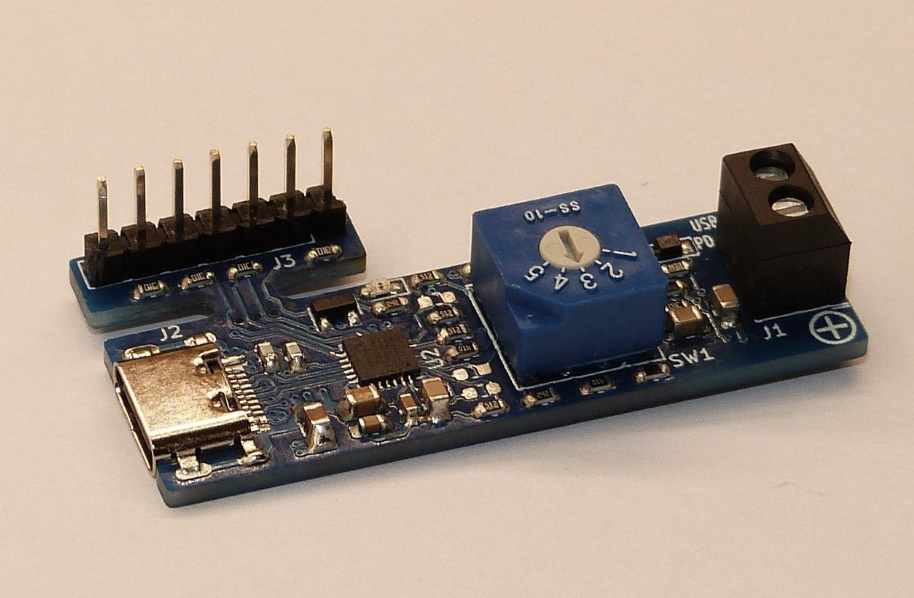
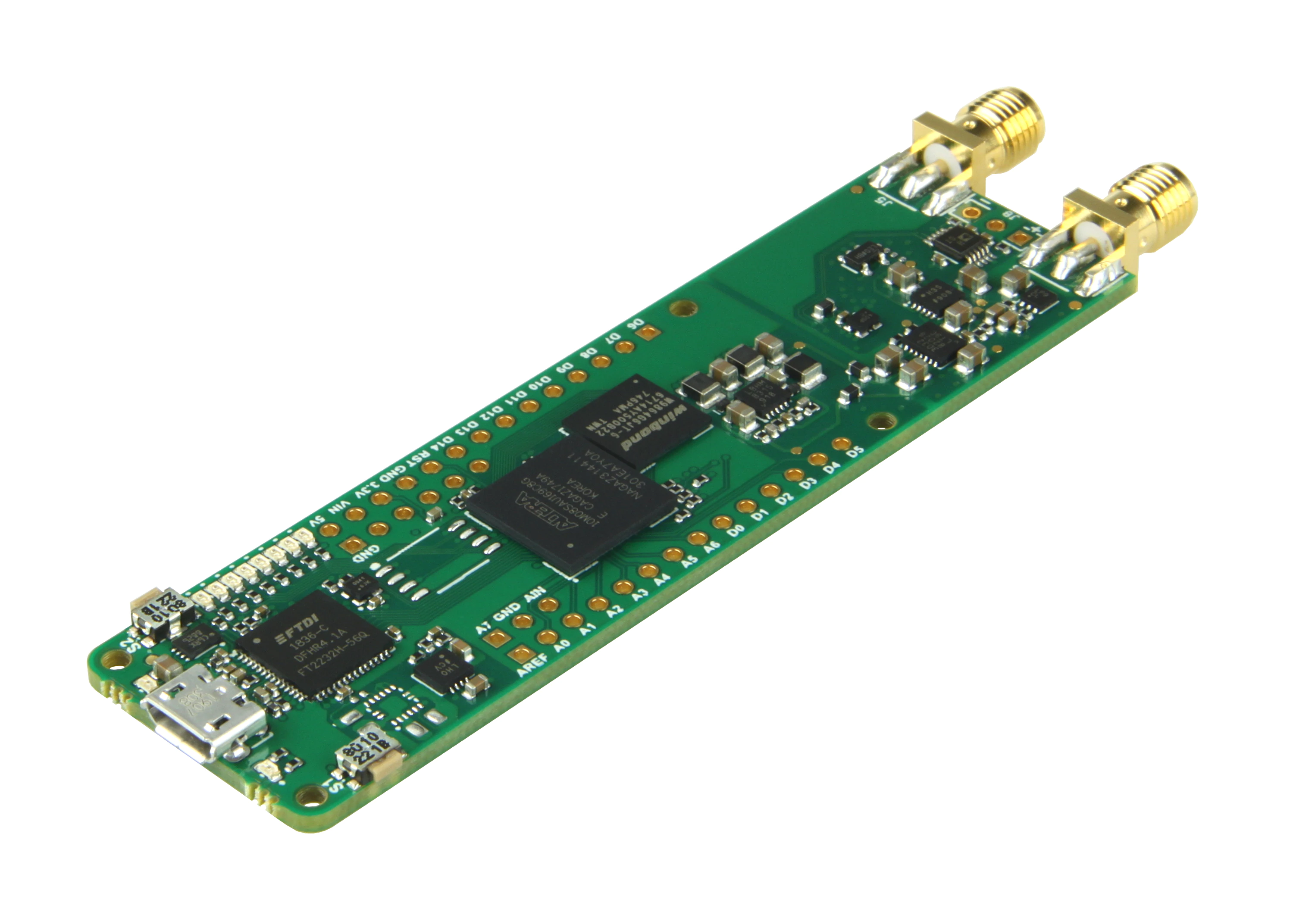
The AnalogMAX-DAQ1, AnalogMAX-DAQ2 and AnalogMAX-DAQ3 each combine an Analog Devices’ high-performance precision data acquisition signal chain and power solution, an Intel MAX 10 FPGA and a memory subsystem comprising up to 64Mb 166MHz SDRAM, 64Mb Quad SPI Flash, and 4Kb EEPROM in a compact 86.5mm x 25mm form factor. With a Micro USB receptacle, 23 GPIOs, and two SMA connectors, these platforms can be deployed in portable instrumentation and desktop equipment such as medical devices, as well as process-controllers and automated test equipment (ATE).

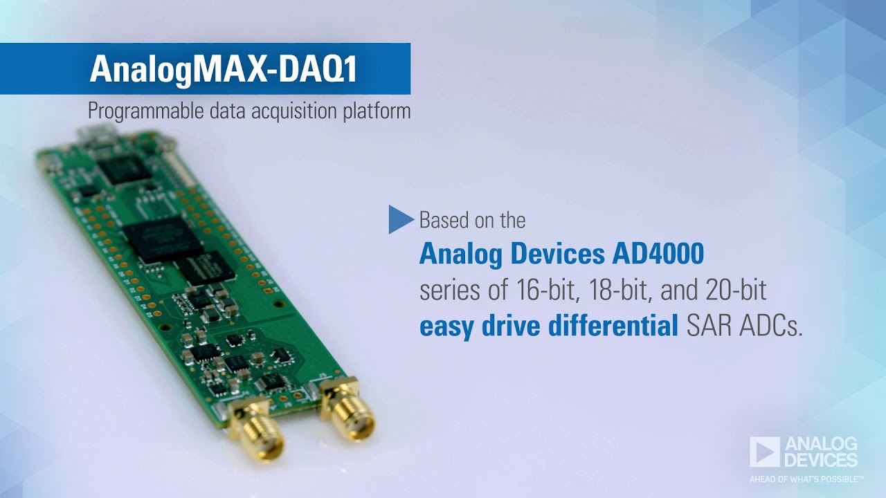
The AnalogMAX-DAQ1 is a high-accuracy programmable data-acquisition platform that integrates a complete precision signal chain for capturing high-frequency signals. This platform is based on the Analog Devices’ AD4003 18-bit 2Msample/s Easy Drive differential SAR ADC (analog-to-digital converter). An AD8251 10MHz programmable-gain instrumentation amplifier and AD8475 funnel amplifier provide low-noise gain and single-ended to differential signal conversion for driving the ADC. This platform can also be used with the pin-compatible AD4001, or AD4020 differential SAR ADC, offering users the choice of 16-, 18-, or 20-bit resolution and throughput from 500ksample/s to 2Msample/s.

Features:

  • Intel® MAX 10 Commercial [10M08SAU169C8G]
  • Package: UBGA-169
  • Speed Grade: C8 (Slowest)
  • Temperature: 0°C to 85°C
  • Package compatible device 10M02…10M16 as assembly variant on request possible
  • SDRAM Memory up to 64Mb, 166MHz
  • Dual High-Speed USB to Multipurpose UART/FIFO IC
  • 64 Mb Quad SPI Flash
  • 4Kb EEPROM Memory
  • 8x User LED
  • Micro USB2 Receptacle 90
  • 18 Bit 2MSPS Analog to Digital Converter
  • 2x SMA Female Connector
  • I/O interface: 23x GPIO
  • Power Supply:
  • 5V
  • Dimension: 86.5mm x 25mm
  • Others:
  • Instrumentation Amplifier
  • Differential Amplifier
  • Operational Amplifier

The AnalogMAX-DAQ2 leverages Analog Devices ADAQ798x 16-Bit μModule data acquisition System-in Package (SiP) solution, which reduces end system component count by combining multiple common signal processing and conditioning blocks into a single device including a low-noise, high-bandwidth ADC driver, a stable reference buffer, and a high-accuracy 16-bit SAR ADC , and efficient power-management circuitry. This platform comes with an option of the 1Msample/s ADAQ7980 or 500ksample/s ADAQ7988 μModule, driven by an AD8251 instrumentation amplifier. The ADAQ798x also integrates critical passive components to ensure specified performance, enabling users to achieve over 90dB typical signal-to-noise ratio (SNR) and -105dB typical total harmonic distortion (THD).

Mini USB-C PD sink board enables Power regulation for any device

The USB-C PD-Sink is a board by Pier 42 that enables any device to be powered from a USB supply. It allows the option to set the voltage at 5V, 9V, 12V, 15V or 20V and allowing current as high as 5A.

The current settings are very flexible in steps of 250mA from 0 to 5A, but this depends on whether the source can limit the current in those small steps. It uses 2oz copper thickness to ensure good current capacity.

The board was built to develop a standard way to use a USB-C power delivery (USB PD) instead of random power adapters. It will prevent the typical USB-C case where your power adapter cannot supply enough current for your load.

No programming or software configuration is needed for the regular operation of the board because all options are set through resistor values. Any type of power connector can be connected to the board through a 2-pin screw terminal or directly soldered into the PCB for projects on a low budget especially during rapid prototyping.

An I2C interface to a microcontroller is available, to access status and control registers. This part of the board is separated through a break-off tab (mouse bits) and can be snapped off. However, it is recommended to score a line along the holes on both sides before snapping off so that you put less stress on the components nearby.

A USB-A connector option at the output end was not included by design since the device could put more than 5 volts through the VBUS pin of the USB cable, which could destroy the device that is plugged in.

Some features of the device are :

  • USB-C PD Power Delivery Sink
  • Selector switch for 5V, 9V, 12V, 15V or 20V
  • Max current 5A, settable in 250mA steps through resistor options
  • Red LED to indicate failed power request
  • I2C telemetry interface to the controller chip
  • Snap off option for a telemetry interface
  • For fixed voltage, the switch can be replaced by wire jumper
  • small form factor to be heat-shrunk as part of the power cable
  • Size 48mm x 15mm (without telemetry interface)
  • Height 12mm with screw terminal and switch, 6mm without.
  • 2oz copper to safely handle 5A
  • Lead-free to be RoHS compliant

The USB-C PD Sink is available now on Tindie for $16, and you can order it with a barrel jack screw terminal for $18 all together.

Arduino Ethernet Shield powered by the PIC32MX controller

Angelu (Elsofgel), a Canadian-based electrical engineer has developed an Arduino shield to implement an SPI to Ethernet Interface (SEI) on the PIC32 microcontroller. While it seems very similar to the Wiznet’s chips, the major difference being that it is a software implementation and the physical layer (PHY) is an external device.

It interfaces the host controller via SPI interface with a clock speed up to 20MHz, and one extra interrupt line. One 8 bit GPIO port and one 15bit GPIO port that can be controlled by the host controller. The SPI implementation has a “Register Monitor Interface” that serially outputs most of the register’s values to a PC application which is very helpful during development.

He also wrote two host controller open-source applications in for the device. The first display’s sensor data like outdoor temperature, sensor location time, power grid frequency e.t.c., which you can find here. The other one just shows a very cute picture of a cat.

“There are three versions of the SEI, one implemented on the PIC32MX664F064 with 20K dedicated to the Ethernet Rx/Tx buffers, one implemented on PIC32MX695F512 with 103k of Rx/Tx buffers and one on PIC32MZ microcontroller that offers symmetric encryption. There is a version of each of the three that connects to a network switch KSZ8863RLL instead the classic PHY chip,” notes Angelu.

Though the PIC32MZ microcontroller implementation is not ready at the moment of writing, he also plans to build a version with VLAN capability.

There is no library for the shield yet, so the host controller accesses the registers directly in the examples above. Furthermore, the cat example is driven by an Xmega controller overclocked to 40MHz and the SPI running at 20MHz while writing, and 10MHz while reading.

The features of the shield include:

  • Extra 8 + 15 I/O pins that can be controlled via the SPI interface
  • Register Monitor Interface via a UART Tx pin that can be useful when debugging the Arduino code
  • 20 kB receive/transmit total buffer memory
  • 4 independent multi-subnet sockets
  • 20MHz SPI mode 0, 1, 2 or 3
  • Protocols: ARP, IPv4, ICMP, UDP, TCP, DHCP
  • PING reply algorithm
  • Interrupt System
  • PHY with Auto MDI-X capability
  • MicroSD socket onboard
  • 3.3 – 5V compatible

The PCB design is open source, and the User manual, schematics, and 3D pdfs are all available on Github. The shield is currently available on Tindie for $22 and some information about it is also available there.

L6983 38 V Step-Down Converter is a synchronous monolithic step-down regulator

STMicroelectronics’ step-down converter is an easy to use synchronous monolithic step-down regulator

STMicroelectronics L6983 Synchronous Step-Down Converter is an easy to use monolithic step-down regulator capable of delivering up to 3A DC to the load. The wide input voltage range makes the device suitable for a broad range of applications. The L6983 is based on a peak current mode architecture. The device is packaged in a QFN16 3×3 with internal compensation, thus minimizing design complexity and size.

The L6983 is available both in low consumption mode (LCM) and low noise mode (LNM) versions. LCM maximizes the efficiency at light-load with controlled output voltage ripple so the device is suitable for battery-powered applications. LNM makes the switching frequency constant and minimizes the output voltage ripple for light load operations, meeting the specification for low noise-sensitive applications. The L6983 allows the switching frequency to be selected in the 200kHz to 2.2MHz range with an optional spread spectrum for improved EMC.

The EN pin provides an enable/disable function. The typical shutdown current is 2µA when disabled. As soon as the EN pin is pulled up, the device is enabled, and the internal 1.3ms soft-start takes place. The L6983 features Power Good open collector that monitors the FB voltage. Pulse-by-pulse current sensing on both power elements implements an effective constant current protection, and thermal shutdown prevents thermal run-away.

Features

  • Two different versions: LCM for high efficiency at light loads and LNM for noise-sensitive applications
  • 200 kHz to 2.2 MHz programmable switching frequency; stable with low-ESR capacitors
  • Operating input voltage: 3.5 V to 38 V
  • Output voltage: 0.85 V to VIN
  • 3 ADC output current
  • Operating quiescent current: 17 μA
  • 2 μA shutdown current
  • Optional spread spectrum for improved EMC

Applications

  • Designed for 24 V buses industrial power systems
  • 24 V battery-powered equipment
  • Decentralized intelligent nodes
  • Sensors and always-on applications

Block Diagram:

more information: www.st.com

Low Power Brushed DC Motor Driver IC from Toshiba in Compact HSOP8 Package

Toshiba Electronic Devices has added the TB67H451FNG Motor Driver IC to its lineup of low power consumption brushed DC motor driver ICs. The new IC comes in the popular pin-assignment HSOP8 package and features automatic return after over-current detection. Over-current detection is a safety function that prevents damage to the IC by turning off the output when the output current exceeds the threshold level due to an overload or other reason.

The previous version of TB67H451FNG is the TB67H450FNG, this device is a latch-type device, where output is turned off indefinitely until the power is recycled or the standby mode is reasserted, whereas the TB67H451FNG has an auto-return function that resumes the operation without any external control. When the overcurrent condition subsides, operation returns to normal.

TB67H451FNG can drive brushed DC motors with a wide range of power supply, from 4.5V to 44V. These ICs can be used in applications like mobile devices and devices with 5V power supply, and industrial devices, home appliances, printers, and banking terminals that require a high power drive of up to 3.5A. For more information about TB67H451FNG, visit the official website Toshiba Electronic Devices and Storage Corporation.

R&S NGP800 Power Supplies Offer up to Four Independent Channels in a Single Instrument

Rohde & Schwarz released the R&S NGP800 family of power supplies, which include two and four channel models. Channels can be operated fully independently or synchronized, and features include a 5” high-resolution touch screen, which also displays detailed statistics. The devices offer voltages up to 250V, currents up to 80A, and power up to 800W. Each channel supplies up to 200W with a maximum of 20A or 64V, also covering 48V automotive and industrial applications.

A tracking function makes it possible for users to adjust voltage and current simultaneously on selected channels, with programmable output delays used to meet specific power-up sequences. The supplied voltage can be ramped up to the required level in any period from 10 ms to a minute. All outputs operate in either constant voltage mode or constant current mode.

It is possible to set up changes in voltage and current level over time, using the QuickArb function, which can simulate unstable power supplies with the R&S NGP800. Using Remote Sensing, users can regulate the voltage directly at the input terminals of the powered device itself, instead of the power supply’s output terminals.

Moreover, the R&S NGP800 includes functions for logging voltage, current and power values over time for all outputs. Data logs can easily be exported as .CSV files for in-depth analysis or documentation needs. The settings for all channels and functions can also be stored and recalled at the touch of a button, and even exported as a file to other R&S NGP800 to duplicate the power setup. All R&S NGP800 power supplies include overcurrent protection, overvoltage protection and overpower protection.

more information: www.rohde-schwarz.com

42V, 15A Synchronous Step-Down DC-DC Regulator

The LT8648S synchronous step-down dc-dc regulator from Analog Devices features second generation Silent Switcher architecture designed to minimize EMI emissions while delivering high efficiency at high switching frequencies. This includes the integration of input and boost capacitors to optimize all the fast current loops inside and make it easy to achieve advertised EMI performance by reducing layout sensitivity.

This performance makes the LT8648S suited for noise sensitive applications and environments. It is expected to be used in automotive and industrial systems as well as general-purpose voltage step-down applications.

The fast, clean, low overshoot switching edges enable high efficiency operation even at high switching frequencies, leading to a small overall solution size. Peak current mode control with a 25ns minimum on-time allows high step down ratios even at high switching frequencies.

Simplified schematic

External compensation via the VC pin allows for fast transient response at high switching frequencies. The VC pin also enables current sharing and a CLKOUT pin enables synchronizing other regulators to the LT8648S.

Burst Mode operation enables low standby current consumption, forced continuous mode can control frequency harmonics across the entire output load range, or spread spectrum operation can further reduce EMI emissions. Soft-start and tracking functionality is accessed via the SS pin, and an accurate input voltage UVLO threshold can be set using the EN/UV pin.

Summary of Features:

  • Silent Switcher ®2 Architecture
    • Ultralow EMI Emissions on Any PCB
    • Eliminates PCB Layout Sensitivity
    • Internal Bypass Capacitors Reduce Radiated EMI
    • Optional Spread Spectrum Modulation
  • High Efficiency at High Frequency
    • Up to 95.5% Efficiency at 1MHz, 12VIN to 5VOUT
    • Up to 93% Efficiency at 2MHz, 12VIN to 5VOUT
  • Wide Input Voltage Range: 3V to 42V
  • 15A Output Current
  • Low Quiescent Current Burst Mode® Operation
    • 100µA IQ Regulating 12VIN to 5VOUT
    • Output Ripple < 10mVP-P
  • External Compensation: Fast Transient Response and Current Sharing
  • Fast Minimum Switch On-Time: 25ns
  • Low Dropout Under All Conditions: 35mV at 1A
  • Forced Continuous Mode
  • Adjustable and Synchronizable: 200kHz to 2.2MHz
  • Output Soft-Start and Power Good
  • Safely Tolerates High Reverse Current
  • Small 36-Lead 7mm × 4mm LQFN Package
  • AEC-Q100 Qualification in Progress
Analog Devices Inc.

New Chip brings ultra-low power WiFi connectivity to IoT devices.

Electrical engineers from the University of California, San Diego recently designed a new portable chip that consumes 5000 less power than the Wi-Fi radios that we have today.

The new chip, which is smaller in size compared with a grain of rice, is said to be ideal for IoT devices, smart home setups, and wearables. With just 28 microwatts of power, the tiny chip can allow devices to connect with existing Wi-Fi networks and transmit data at a rate of two megabits per second within a range of 21 meters.

Smart devices, mobile phones and even small cameras or various sensors to this chip, it can directly send data from these devices to a Wi-Fi access point near you. You don’t need to buy anything else and it could last for years on a single coin cell battery,” explains Dinesh Bharadia who is one of Professors of UC San Diego electrical and computer engineering department working on the chip.

The Wi-Fi radio on the chip is said to use far less power compared with the popular commercial WiFi radios, hence Wi-Fi compatible devices can last for years instead of just hours, even when unplugged. This definitely beats the popular commercial WiFi devices as they will need either large batteries or other external power sources to run for as long as the current chips as it takes 100s of milliwatts just to pair devices.

Data transmission by the device is done by taking incoming Wi-Fi signals from a nearby device, modify and encode its own data onto them, and then reflect the new signals onto a different Wi-Fi channel to another device. This process in technical terms is known as backscattering and it simply implies transmitting data by piggybacking data using signals of already connected devices. This feature allows the chip to, not only save on power, but also increases it’s range as it spreads as the WiFi signal continues to spread.

The Team Demonstrating the Backscattering Process

 “This WiFi radio uses low enough power that we can now start thinking about new application spaces where you no longer need to plug IoT devices into the wall. This could unleash smaller, fully wireless IoT setups. It could also allow you to connect devices that are not currently connected – things that cannot meet the power demands of current Wi-Fi radios, like a smoke alarm – and not have a huge burden on battery replacement” said Patrick Mercier, another computer and electrical engineering professor who co-led the work with Bharadia.

This team’s improvement to technology is nothing short of interesting as it makes the whole system smaller and more efficient, who knows what the next big thing from them would be.

ONiO.zero RISC-V Microcontroller Functions On Harvested Energy

ONiO, a Norwegian healthcare-focused Internet of Things (IoT) expert has unveiled ONiO.zero, an ultra-low-power RISC-V-based microcontroller capable of operating solely from harvested energy — without needing a battery, capacitor, or any other means of energy storage. The company says “ONiO.zero is an ultra-low-power wireless MCU that uses energy harvesting technology.” This indicates that the ONiO.zero solely functions on energy harnessed from its surroundings. With no coin cell, no supercap, no lithium, no battery at all, the ONiO.zero is still a ton of power.

The company says:

“Battery based solutions come with the inevitable caveat of battery replacement, which translates to an incremental cost, throughout their ownership. ONiO.zero circumvents this pain point and slashes the cost of ownership. It can be used to power sensors and devices for years, without having to spare a thought about maintenance — deploy and forget. ONiO.zero is self-powered and supports a wide range of power sources from multi-frequency RF bands supporting GSM and ISM to optional external sources like solar, piezoelectric, thermal and voltaic cells.”

Having no battery means fewer components and a smaller design, which can easily be integrated into a wide range of solutions – be it fabrics, jewelry, watches, wearable medical devices, livestock or building sensors. More importantly, this makes for a cleaner, more eco-friendly solution.

The microcontroller is based on the open source RISC-V instruction set architecture, specifically the RV32EMC, which runs at up to 24MHz when fed with 1.8V. The controller can also operate at a lower voltage when required: 1V offers 6MHz, and 0.8V offers 1MHz. According to the company, the chip will continue to run – albeit at ever-decreasing speeds – as low as 450mV. There’s 1kB of mask ROM and 2kB of RAM included, along with 8-32kB of ultra-low-power flash storage capable of 100,000 write cycles and readable down to 850mV. The ONiO.zero also features a crystal-free Bluetooth Low Energy (BLE) transmitter, which operates at voltages as low as 850mV, an IEEE 802.15.4 ultra-wide-band (UWB) transmitter which operates in the 3.5-10GHz band, and an optional 433MHz MICS radio transmitter for industrial, scientific, and medical band use.

The chip’s energy is a result of an internal radio-frequency rectifier, which harvests power from the 800/900/1800 and 1900/2400MHz bands (ISM and GSM). In the case of environments without sufficient radio-frequency energy to effectively power the chip, the “internal power factory” supports photovoltaic cells down to 400mV, piezoelectric, and thermal sources from 1.8V to 3.6V. More information on ONiO.zero can be found in the datasheet available on the official product page.

Free Elektor Article: Using E-paper with the Arduino

Electronic paper — a.k.a. e-paper — is an unusual type of display. Once a picture (or text) is displayed, no further energy is required to maintain the display. Energy is only required to change the display. This is very useful in applications where the amount of available energy is limited. In this article we describe a practical application of such a display and control it with an Arduino/Elektor Uno.

  • Original publication: Elektor Magazine 6/2016 (November & December) on page 74
  • Authors: Niek Laskarzewski and Thijs Beckers
  • Original article production number: 160097
  • Free download expires: Friday 28 February 2020
  • Bare PCB: available, see PRODUCTS below
  • e-paper display: available, see PRODUCTS below

Like what you’re seeing? Then go to the article page and download a pdf copy of the full, original article. Downloading is free from Friday 21 February to Friday 28 February 2020.

TOP PCB Companies