One of the best things about being a maker is the ability to make your own tools. We have covered the development of several electronics tools in past, from voltmeters to battery testers. For today’s tutorial, we will add another tool to the list by examining the development of a Miliohm meter made by danielrp @ www.instructables.com
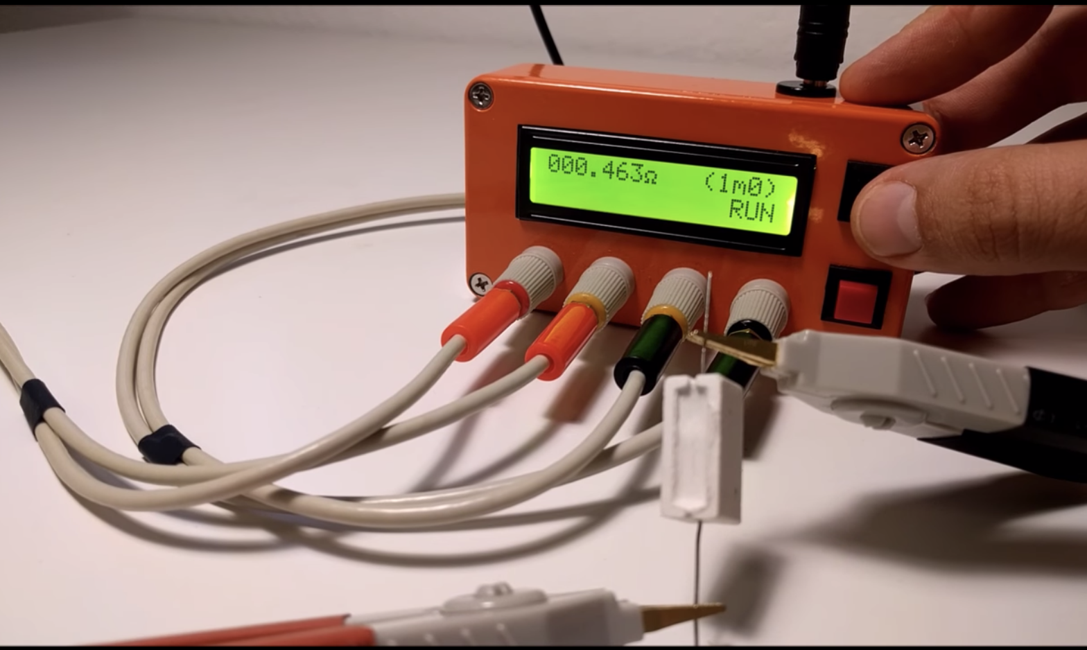
A milliohm meter is a device used in determining the resistance of small resistors, PCB traces, motor coils, inductance coils, and transformer coils, or calculate things like the length of wires. It provides a resolution, not built into regular multimeters, making it easy to get accurate readings in the milliohm range.
There are quite a number of Miliohmeter builds on the internet, but today’s tutorial will chronicle the efforts of instructable user Danielrp. Daniel’s version of the meter is based on a precision current sink and a high-resolution ADC controlled by an Arduino Nano. The current sink is based on the LT3092 precision current source/sink which, using a network of resistors and transistors is set to function as a sink. For the ADC, the high resolution, MCP3422A0 I2C ADC is used. Just one of the channels of the ADC is used, and it is connected differentially to the Resistor under test “S+ S-“. The MCP3422 is configured as 18bit but as S+ is always going to be greater than S-, the effective resolution is 17bit.
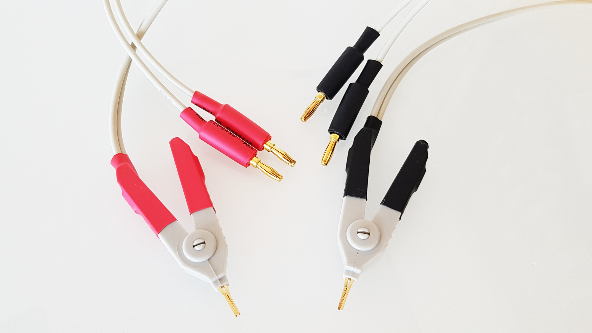
To reduce the influence of the resistance of the test leads on the measurement, the devices use Kelvin connectors as leads to connect the resistor under test to the measurement point.
The measurement range of the device include:
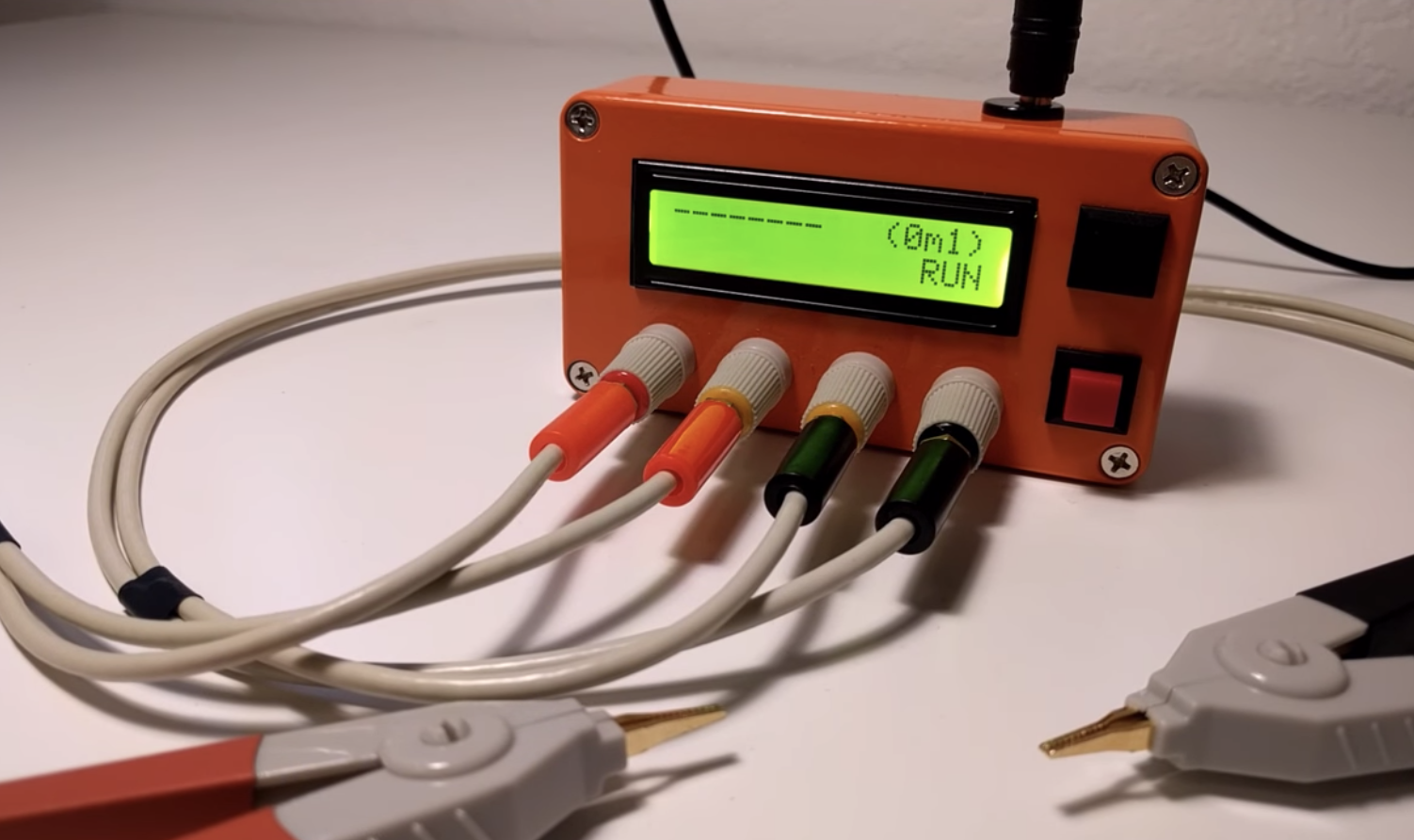
- Scale 0m1: 0.1mOhm to 12.9999 Ohm.
- Scale 1m0: 1mOhm to 129.999 Ohm.
- Scale 10m: 10mOhm to 1299.99 Ohm.
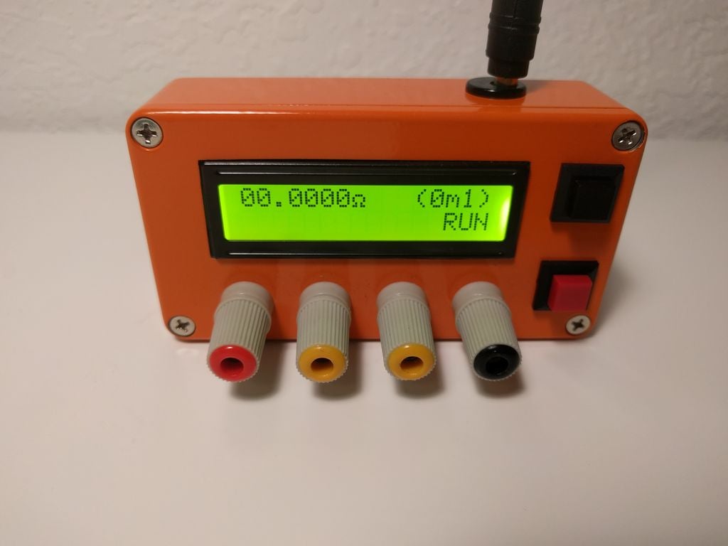
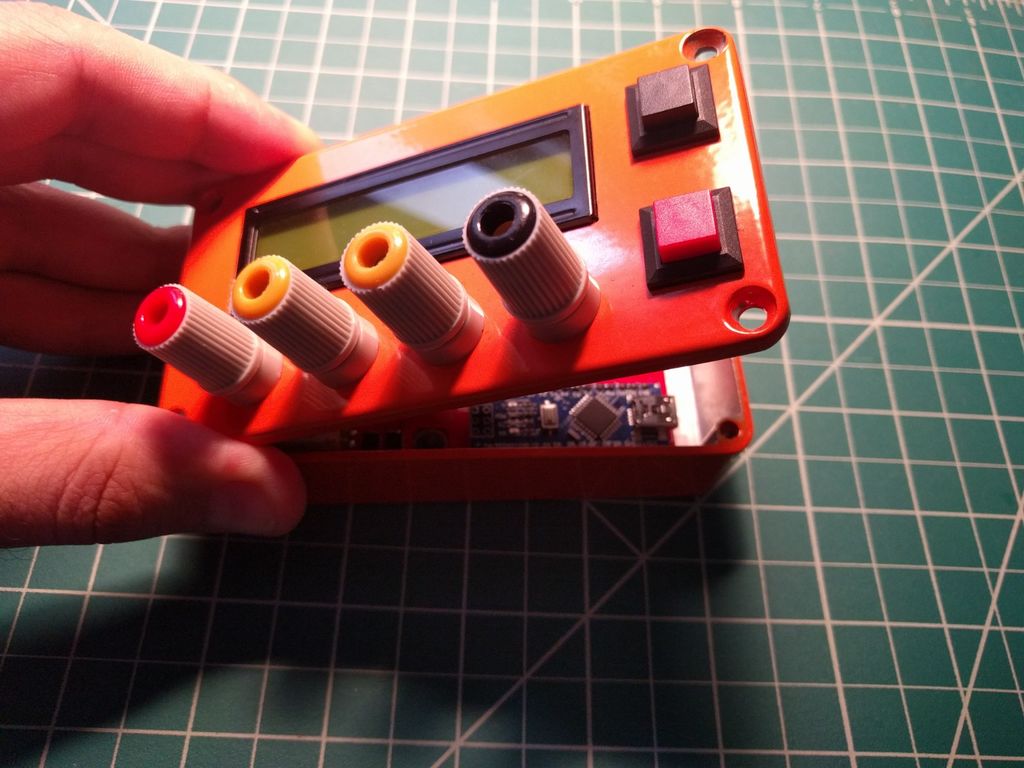
Users can make the selection between the above measurement ranges by using one of the two push buttons on the device. Visual feedback on the selections and meter readings is provided to users via a 16×2 LCD display, and the entire project is enclosed in an orange Hammond 1590B aluminum box to make it handy and presentable.
Ready to build? let’s dive in.
Required Components
Due to the bulkiness, the complete list of components required to build the project is attached under the download section. However, some of the key components to be used include:
- Arduino Nano
- 16×2 LCD Display
- ULN2003A
- LT3092EST
- MCP3422A0
- Kelvin Connectors
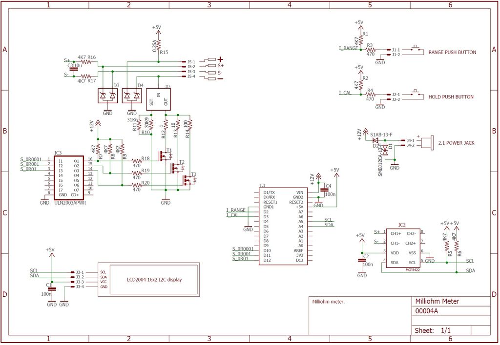
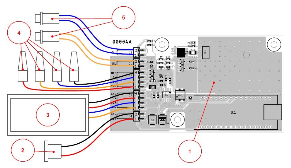
Schematics
Due to the complex nature of the project, implementing on a breadboard will not only be time-consuming but also make the project susceptible to errors. To prevent this, the project was implemented on a PCB designed with Eagle. The schematics showing how the components are connected on the PCB is provided below:
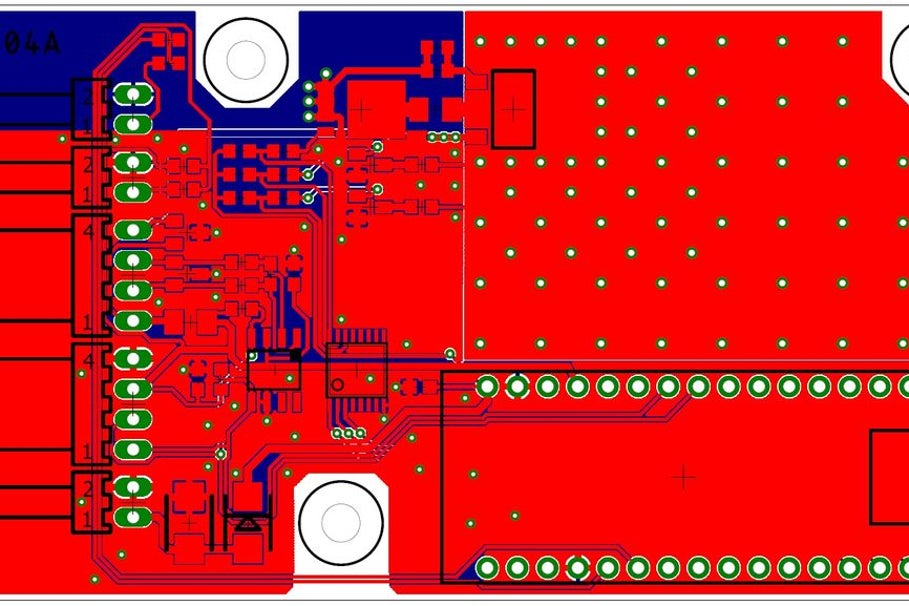
The PCB, developed from the schematics, looks like the image below:
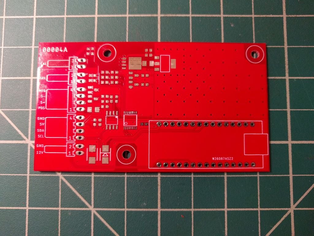
and the final board after manufacturing is shown in the image below.
Both the schematics and PCB files are attached to the BOM under the download section. It should make modifying the project for your personal use a bit easier.
Enclosure and Assembly
The PCB approach was adopted to make the project presentable and useful and to take things even further, DanielrP developed an enclosure for the project.
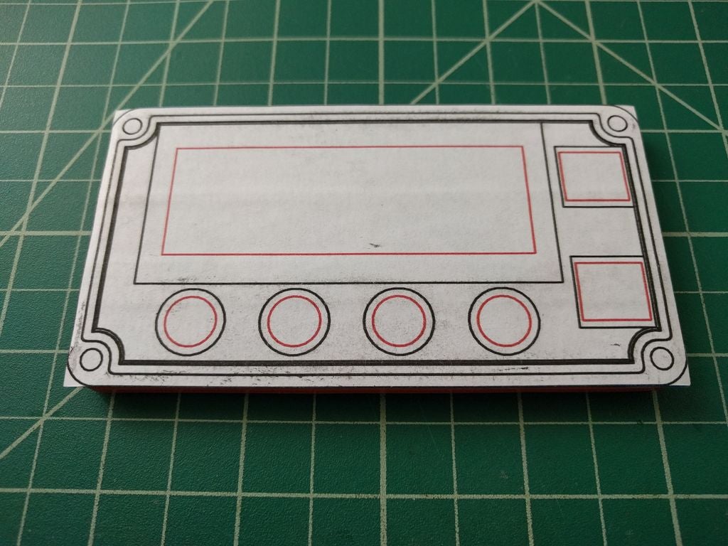
The modification to the Aluminium enclosure box was designed with Inkscape and the design files, along with the stencil are attached under the download section.
Follow the steps below to create the enclosure.
1. Cover the top side of the aluminum box with painter tape. Then cut the stencil for the front cover and glue it to the painter’s tape.
2. Next, mark the positions for the holes and drill holes to allow the fret saw or coping saw blade get into the internal cuts.
3. Cut all the shapes.
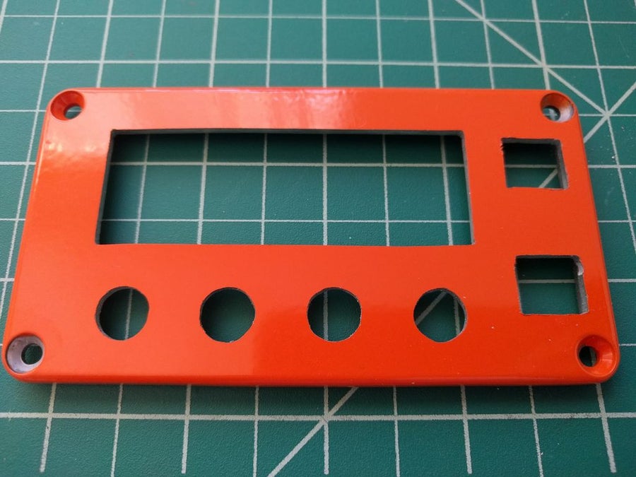
4. Trim with files, then remove the stencil and the painter’s tape.
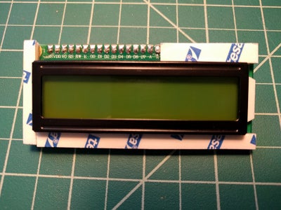
5. Install the pushbuttons along and the screen using double-sided tape or hot glue.
6. With the cover done, on the box itself, mark the position of the holes for the (screws). Center punch the holes.
7. With all the components installed, the top/cover should look like the image below.
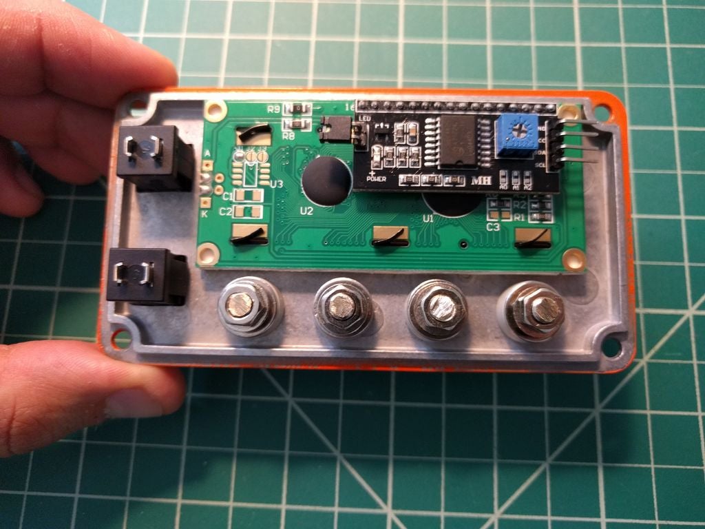
Before coupling together the enclosure, it might be smart to first get some components of the PCB in place. Since most of the components used for the PCB are SMT types, mounting them on the PCB will require the use of a hot-air gun or the use of a regular soldering iron along with a fine-tip tweezer, some solder wick, and a 0.02″ solder.
The image below provides a broad overview of where some of the components go on the PCB.
Since the kelvin connectors and switches are only useful on the outside of the enclosure, they will be connected to the PCB via jumper wires as shown above.
With the PCB and the box now ready, install the PCB in the box and connect the pushbuttons and kelvin connectors.
To make it easy to upload code to the setup when completed, you can open a small hole close to the USB port on the Nano, so a USB cord can be easily connected to it.
With this complete, we are now ready to write the code for the project.
Code
The algorithm behind the code for the project is quite complex. We set the scale for the project by driving the set pins connected to the ULN2003. The scale along with the mode (which is determined by the status of the pushbuttons), is then taken into account and the MCP3422 is read to obtain the resistance value and display it on the LCD.
Since the sketch is already a complex one, to reduce the complexity a bit, a number of libraries were used, including; the Wire.h library, the LiquidCrystal_I2C library, and the EEPROM library. The wire library was used to facilitate I2C Communication between the Arduino and the two I2C components of the project; the LCD and the MCP3422. The LiquidCrystal_I2C library, on the other hand, helped with interfacing with the LCD, while the EEPROM Library was used in accessing the EEPROM on the Arduino to store information about the mode and meter scale.
The Wire and EEPROM libraries come preloaded with the Arduino IDE, while the LiquidCrystal_I2C library can either be installed via the link attached to it or by installing it via the Arduino Library Manager.
As usual, I will do a quick run down and explain some snippets/parts of the Sketch. The code is quite bulky and might be difficult to cover all of it but luckily, Daniel did a good job with comments on each line of code so it should be easy to follow it.
We start the sketch by including all the libraries we will be using.
Next, we specify the dimensions of the display and create macros for the scale. This basically sets the status of pins involved with setting the scale.
//LCD display parameters
#define N_ROWS 2u
#define N_COLS 16u

//General parameters
#define DEBOUNCEHARDNESS 10u

//Macros
//Scale

//0.0001ohm - 156mA
#define SCALE_01    digitalWrite(10, LOW); \
  digitalWrite(11, HIGH); \
  digitalWrite(12, HIGH); \
  pinMode(10, OUTPUT); \
  pinMode(11, OUTPUT); \
  pinMode(12, OUTPUT)
//0.001ohm - 15.6mA
#define SCALE_1    digitalWrite(11, LOW); \
  digitalWrite(10, HIGH); \
  digitalWrite(12, HIGH); \
  pinMode(10, OUTPUT); \
  pinMode(11, OUTPUT); \
  pinMode(12, OUTPUT)
//0.01ohm - 1.56mA
#define SCALE_10    digitalWrite(12, LOW); \
  digitalWrite(11, HIGH); \
  digitalWrite(10, HIGH); \
  pinMode(10, OUTPUT); \
  pinMode(11, OUTPUT); \
  pinMode(12, OUTPUT)
Next, create macros for the Arduino built-in led, which will be used to provide visual feedback as regards the status.
We follow this with a configuration of the pushbuttons. One to turn it on or off and the other to take it in and out of calibration mode.
Next, we declare some of the variables that we will be using for the MCP3422 related data. We specify variables to hold the channels, the slave address and other things.
//MCP3422
#define MCP3422_CH1 0x00
#define MCP3422_CH2 0x01
#define MCP3422_SR 0x03 //3.75 SPS (18bit)
#define MCP3422_GAIN 0x00 //x1
#define MCP3422_CR_STARTONESHOT 0x80 // /RDY bit = 1, /O/C bit = 0
#define MCP3422_CR_READY 0x80        // /RDY bit mask
#define MCP3422_NCH 2u    //Number of channels available
#define MCP3422_ADD 0x68  //Slave address
Next, we create a string of messages that will be displayed.
//Messages
const char strHOLD[5] = "HOLD";
const char strRUN[5] = " RUN";
const char strScale0m1[6] = "(0m1)";
const char strScale1m0[6] = "(1m0)";
const char strScale10m[6] = "(10m)";
const char strScaleAuto[7] = "(Auto)";
const char strFullScale[9] = "--------";
followed by a specification of the EEPROM address where different types of data are stored.
//EEPROM Addresses
#define EE_U8MODE       0x0000
#define EE_U8SCALERUN   0x0002
#define EE_U8SCALEHOLD  0x0004
#define EE_U32MEASHOLD  0x0006
Next, we create some type of variables
//MCP3422 machine states
enum eMCP3422ReadStates_t
{
  eMS_WaitCurrent = 0,
  eMS_WaitVoltage = 1
};
Create an instance of the LiquidCrystal_I2C library, and create some other general variables.
LiquidCrystal_I2C lcd(0x3F, 2, 1, 0, 4, 5, 6, 7, 3, POSITIVE); // Addr, En, Rw, Rs, d4, d5, d6, d7, backlighpin, polarity (As descrived in the ebay link but with 0x3F address instead of 0x20)

//General variables
bool bIsHoldMode = false;
uint8_t u8HoldScale = 0;
uint32_t u32HoldValue = 0;
uint8_t u8CurrentScale = 0;         //Current Scale
uint32_t u32CurrentMeasurement = 0;       //Last conversion value from MCP3422
bool bMCP3422ValIsPositive = true;  //Last conversion sign, in this circuit it's always positive

bool bSCALEPressed = false;      //State of On push button
bool bLastSCALEPressed = false;  //Last state of On push button, used for flange detection
bool bCALPressed = false;     //State of Off push button
bool bLastCALPressed = false; //Last state of Off push button, used for flange detection
uint8_t u8SCALEDebounce = 0;     //Debounce counter for On push button
uint8_t u8CALDebounce = 0;    //Debounce counter for Off push button
Next, is the void setup() function. We start by checking what the current scale is and then setting the scale to that value.
void setup()
{
  if(!eeReadU8(EE_U8SCALERUN , u8CurrentScale))
  {
    eeStoreU8(EE_U8SCALERUN, 0);
    u8CurrentScale = 0;
  }
  changeScale(u8CurrentScale);
Next, we call the setupDisplay() function to initialize the LCD and display a sort of splash screen.
setupDisplay();
The above is followed by setting the speed of I2C communication, turning the backlight of the LCD high, and rounding up the setup function by initializing Serial communication so the serial monitor can be used for debugging purposes.
  Wire.setClock(400000);  //Speed for both display and MCP3422
  lcd.setBacklight(HIGH);
  Serial.begin(9600);


}
Up next is the void loop() function. The function starts with a line of code to obtain an update on the status of the pushbuttons, the modes and scale among others.
void loop()
{
  updateInputs(); //Read  pushbuttons, update modes and change scale
This is followed by an if statement which checks if the device is in hold mode. If the device is in hold mode, the scale and the measurement are obtained but if it’s not(run mode), Update bufferA with the “RUN” text, Read the RUN scale, Set the RUN scale in the current sink, check if data is available from the MCP3422, and start a new data conversion on the channel.
if(true == eeIsHoldMode())
  {//Hold Mode
    writeString(1u, 12u, strHOLD);                    //Update bufferA with the "HOLD" text
    eeReadU8(EE_U8SCALEHOLD, u8CurrentScale);         //Read the HOLD scale
    eeReadU32(EE_U32MEASHOLD, u32CurrentMeasurement); //Read the HOLD measurement
  }
  else
  {//Run Mode
    writeString(1u, 12u, strRUN);                     //Update bufferA with the "RUN" text
    eeReadU8(EE_U8SCALERUN, u8CurrentScale);          //Read the RUN scale
    changeScale(u8CurrentScale);                      //Set the RUN scale in the current sink
    //Read the ADC if a new measurement is available.
    if(MCP3422_IsDataAndRead(u32CurrentMeasurement, bMCP3422ValIsPositive))
    {//New conversion available
      if(false == bMCP3422ValIsPositive)
      {
        u32CurrentMeasurement = 0;
      }
      MCP3422_StartConversion(MCP3422_CH1);   //Restart conversion
    }
  }
Finally, the display buffer is updated, and the value is displayed on the LCD using the updateDisplay() function which wraps up the loop().
  updateDisplayBuffer();                              //Update the rest of BufferA
  updateDisplay();                                    //Write the necessary chars in the display
}
The void loop() and void setup() discussed above contain very few lines of code because the majority of the work is done in several other functions. From the function which handles data conversion on the MCP3422 ADC to the one used in setting the scale and the one used in updating the display, all of this function play an important role and while its a bit difficult to go over them one after the other because of how bulky it will make the tutorial, the code to implement them is properly commented by Danielrp so it should be easy to follow.
The complete sketch is attached in the zip file under the download section below.
Demo
With the code complete and the hardware in place, connect the device to your computer and upload the code to it.
After a while, you should see the display come up as shown in the image below.
On connecting a milliohm resistor to the leads, you should see the value of that resistor displayed.
That’s it.
To learn more about the project, you can watch this video made by danielrp.