Nexperia Releases its 0.57 mili-Ohm Product in LFPAK56 Packaging

Nexperia announced the release of its lowest-ever RDS(on) power MOSFET, the PSMNR51-25YLH, exhibits a value of 0.57mΩ at 25V. Based on NextPowerS3 technology, this performance doesn’t compromise other parameters such as maximum drain current (ID(max)), Safe Operating Area (SOA), or gate charge QG.

Features

  • 100% avalanche tested at I(AS) = 190 A
  • Optimized for low RDSon
  • Low leakage < 1 μA at 25 °C
  • Low spiking and ringing for low EMI designs
  • Optimized for 4.5 V gate drive
  • Copper-clip for low parasitic inductance and resistance
  • High-reliability LFPAK package, qualified to 175 °C
  • Wave solderable; exposed leads for optimal solder coverage and visual solder inspection

Nexperia’s PSMNR51-25YLH MOSFET offers a maximum drain current rating up to 380 Amps, especially important in motor control applications where motor-stall can result in very high current surges for short periods. The device is packaged in LFPAK56, Nexperia’s 5mm x 6mm Power-SO8 compatible package, with a copper-clip construction that absorbs thermal stresses.

www.nexperia.com

PicoScope 4-Channel 16GHz Sampler-Extended Real-Time Oscilloscopes

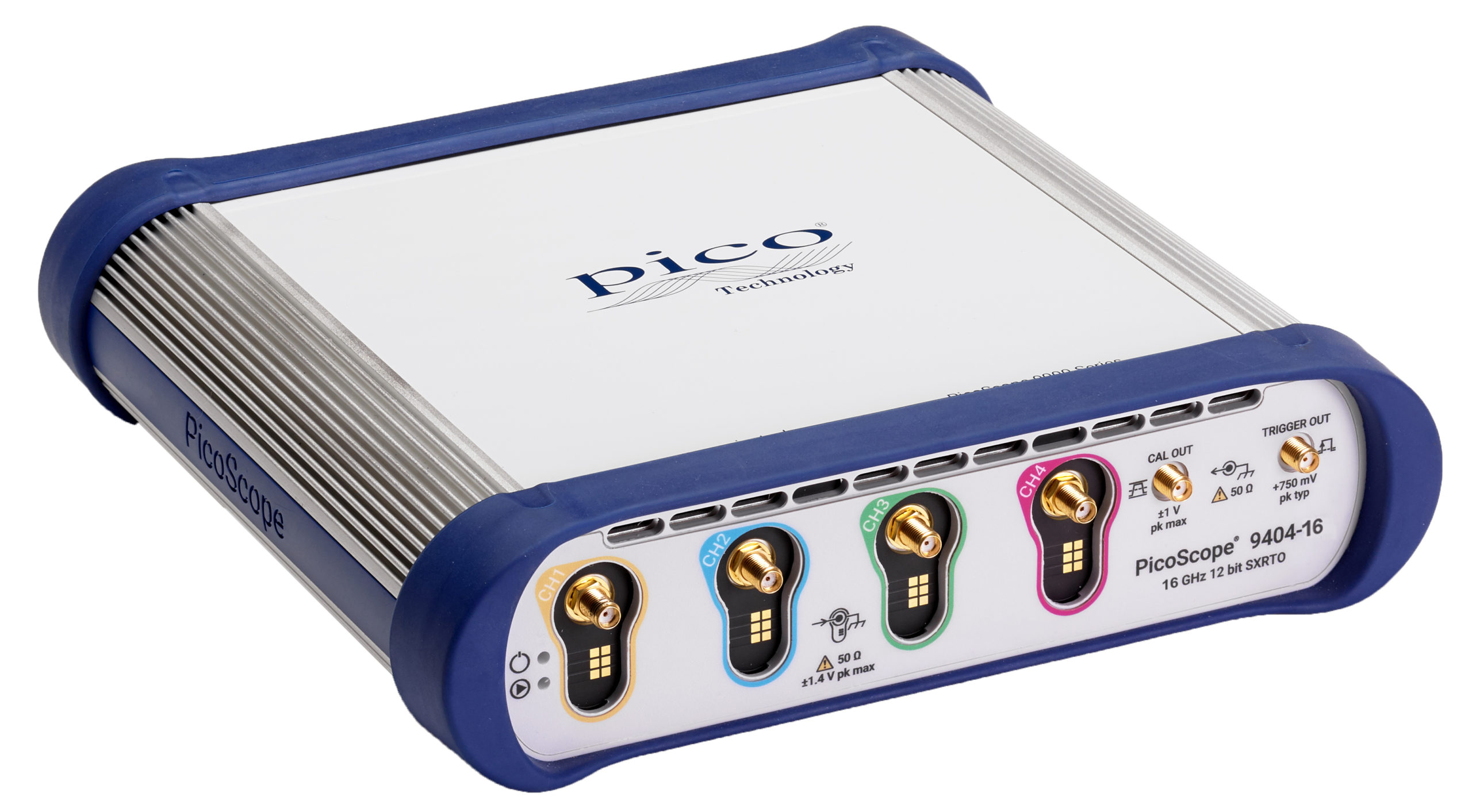
The PicoScope 9404-16 brings very high-speed performance at less than half the cost of other traditional benchtop solutions with four high-resolution 12-bit channels driven by up to 5TS/s (0.2ps) equivalent-time sampling

Saelig Company, Inc. has introduced the PicoScope 9404-16 SXRTO, a 16GHz sampler-extended real-time oscilloscope which extends the range of a preceding  5GHz model. Designed to analyze repetitive or clock-derived signals, it features four high-resolution 12-bit channels driven by up to 5TS/s (0.2ps) equivalent-time sampling (ETS). The wide-band inputs can accurately measure transitions as fast as 22ps, pulses down to 45ps wide, and permits clock performance and eye diagram analysis of up to 11Gb/s gigabit signals (to third harmonic). In addition, the real-time broadband sampling modes can support analysis for other common RF signals such as wireless frequencies of 900MHz, 2.4 and 5.5GHz and upwards.  Pico’s SXRTO instrument architecture reduces the cost of broadband time-domain sampling for repetitive signal or clock-related applications.

In contrast to “sampling oscilloscopes”, the ETS technique supports trigger and pre-trigger capture and the familiarity, convenience and ease of real-time oscilloscope operation. Pico’s SXRTO technology seamlessly transitions to single-event, real-time waveform capture at sampling rates at and below 500MS/s.  Both sampling modes capture to memory of 250,000 samples (single channel).  This is particularly valuable for the capture of slower system signals, modulation envelopes, and repeating pulse or data patterns, for example.

This USB-controlled PicoScope 9404-16 is supplied with PicoSample 4 software. A free touch-compatible GUI controls the instrument and presents waveforms, measurements and statistics on an attached PC display. There is full support for available Windows display resolutions, allowing the inspection of waveform detail or presentation of measurements, for example on 4k monitors or projection, or across multiple monitors.

A wide range of automated and user-configurable signal integrity measurements, mathematics, statistical views and limits test facilities are included for validation and trending of pulse and timing performance, jitter, RZ and NRZ eye diagrams. Industry-standard communications mask tests such as PCIe, GB Ethernet and Serial ATA are included as standard.  PicoConnect® 900 Series gigabit and microwave passive test probes are recommended for use with the 9404, offering a range of bandwidths, division ratios and AC and DC coupling for diverse applications. The PicoScope 9404 has an active SMA interface to support future configurations and accessories on this product architecture.

The 9404-16 is compact enough to place on a workbench in close proximity to a device under test.  Made by Pico Technology, Europe’s award-winning test and measurement manufacturer, the PicoScope 9404-16 16GHz oscilloscope is available now from Saelig Company, Inc. their USA technical distributor.

ST-5S Smart Tweezers™ for On-board L/C/R Measurements and PCB Testing

This intelligent measurement tool is a new type of handheld LCR meter that can quickly test, identify, and measure board-mounted surface-mount and leaded devices without the need to remove them from a circuit board.

Saelig Company, Inc. has introduced the ST-5S Smart Tweezers™ for on-board inductance, capacitance, and resistance measurements and PCB testing.  The ST-5S tweezers are a valuable solution for quickly testing and identifying surface mount devices, as well as for troubleshooting complex electronic PCBs. Its unique mechanical and electronic design combines a pair of precise gold-plated tweezers and a digital LCR meter in compact, lightweight, battery-powered instrument.  Smart Tweezers™ automatically detects L, C, or R measurements and selects the correct measurement range and test frequency for high accuracy readings. Component type, value, and more detailed component analysis, such as Z and ESR, are all displayed on the instrument’s OLED display.

Surface mount devices are very small and have no wire leads, making it more difficult to test and identify SMDs than conventional leaded components. Smart Tweezers™ also gives users an easy way to sort tiny, loose components. Precise tips reliably contact even the smallest SMD components and take measurements from board-mounted devices. Smart Tweezers™ can also be used to test conventional components with wire leads that may not be long enough to insert into conventional test terminals. The integrated, insulated measurement head allows the operator to use one hand (left or right) for measurements to simplify probe placement tasks.

The ST-5S is for built for professional engineers since it comes with a NIST-traceable calibration certificate. The ST-5S allows users to change the test signal (with 0.5 and 1.0 Vrms), as well as variable tolerances of 1%, 5%, 10%, and 20%. This device also performs continuity and diode testing and shows active and reactive impedance component readings on the display.   A feature that saves time for users is that a semi-automatic offset subtraction feature automatically removes parasitic readings after set-up. The ST-5S is controlled by joystick-like navigation; pushing the button directionally will change the test mode, test signal, etc., and pressing the joystick directly opens a menu to allow more customized measurements and features such as changing the screen orientation.

Swiss-made by Ideal-Tek, a recognized leader in precision handheld assembly tools, ST-5S Smart Tweezers™ are available now from Saelig Company, Inc. their USA technical distributor.

M100PFS – PolarFire RISC-V SoC-FPGA Module

The M100PFS is based on the PolarFire SoC FPGA architecture by Microsemi and combines high-performance 64-bit RISC-V cores with outstanding FPGA technology. The platform integrates a hardened real-time, Linux capable, RISC-V-based MPU subsystem on the mid-range PolarFire FPGA family, bringing low power consumption, thermal efficiency and defence grade security to embedded systems.

The RISC-V CPU micro-architecture implementation is a simple 5 stage, single issue, in-order pipeline that doesn’t suffer from the Meltdown and Spectre exploits found in common out-of-order machines. All five CPU cores are coherent with the memory subsystem allowing a versatile mix of deterministic real time systems and Linux in a single multi-core CPU cluster.

Block Diagram

Features:

  • Microsemi PolarFire SoC FPGA
      • MPFS025T
        23KLE, 68 math blocks, 4x SERDES 12.5Gbit/s, 2x PCIe root port/end point
      • MPFS095T, available on request
        93KLE, 292 math blocks, 4x SERDES 12.5Gbit/s, 2x PCIe root port/end point
      • MPFS160T, available on request
        161KLE, 498 math blocks, 8x SERDES 12.5Gbit/s, 2x PCIe root port/end point
      • MPFS250T
        254KLE, 784 math blocks, 16x SERDES 12.5Gbit/s, 2x PCIe root port/end point
  • Quad 64-bit RV64GC cores, 667 MHz
  • 64-bit RV64IMAC monitor core, 667 MHz
  • Processor I/O
    • 2x Gigabit Ethernet
    • 1x USB 2.0 OTG
    • 1x MMC 5.1 SD/SDIO
    • 2x CAN 2.0 A and B
    • Execute in place Quad SPI flash controller
    • 5x multi-mode UARTs
    • 2x SPI, 2 I2C
    • RTC, GPIO
    • 5x watchdog timers
    • timers
  • Processor to FPGA Interconnect
    • 2 64-bit AXI4 processor-to-fabric interfaces
    • 3 64-bit AXI4 fabric-to-processor interfaces
    • 1 32-bit APB processor-to-fabric interface
  • 1/2/4 GByte LPDDR4 RAM dedicated to the HMS
  • 1/2/4 GByte LPDDR4 RAM dedicated to the FPGA
  • 32 Mbit NOR Flash
  • 4 – 64 GByte eMMC memory
  • Clock distribution
  • default configuration:
    • Gigabit Ethernet
    • UART
    • CAN
    • SPI
    • I²C
    • USB
  • single 3,3V supply
  • size 74mmx42mm
  • 2 x Samtec QSH-090-01-F-D-A board-to-board interconnect

Schedule & Availability

The M100PFS are currently under development, first boards are to be expected appr. in Q3/2020

5V/2A Synchronous DC-DC Converter IC Evaluation Kit

The MAX17662BEVKITB# evaluation kit (EV kit) from Maxim Integrated Products provides a proven design to evaluate the MAX17662B high-efficiency, synchronous step-down dc-dc converter. The EV kit provides 5V/2A at the output from a 6.5V to 36V input supply.

Applications are expected to include base station power supplies, distributed supply regulation, general-purpose point-of-load, high-voltage single-board systems, industrial control power supplies, wall transformer regulation, and so on.

The switching frequency of the EV kit is preset to 500kHz for optimum efficiency and component size. The EV kit features adjustable input under-voltage lockout, adjustable soft-start, open-drain active-low RESET signal.

The EV kit also provides a good layout example, which is optimized for conducted, radiated EMI, and thermal performance.

Hot Plug-In and Long Input Cables

The MAX17662BEVKITB# PCB layout provides an optional electrolytic capacitor (C6 = 47μF/50V). This capacitor limits the peak voltage at the input of the MAX17662B when the dc input source is “hot-plugged” to the EV kit input terminals with long input cables. The equivalent series resistance (ESR) of the electrolytic capacitor dampens the oscillations caused by interaction of the inductance of the long input cables, and the ceramic capacitors at the buck converter input.

Summary of Key Features

  • Operates from a 6.5V to 36V Input Supply
  • 5V Output Voltage
  • Delivers Up to 2A Output Current
  • 500kHz Switching Frequency
  • Enable/Undervoltage Lockout Input, Resistor- Programmable UVLO Threshold
  • Adjustable Soft-Start Time
  • Open-Drain Active-Low RESET Output
  • Overcurrent and Overtemperature Protection
  • Proven PCB Layout
  • Fully Assembled and Tested
  • Compliance with CISPR22(EN55022) Class B Conducted and Radiated Emissions

Electromagnetic Interference

Compliance to conducted emissions (CE) standards requires an EMI filter at the input of a switching power converter. The EMI filter attenuates high-frequency currents drawn by the switching power converter, and limits the noise injected back into the input power source. The MAX17662BEVKITB# has designated footprints on the EV kit for placement of EMI filter components. Use of these filter components results in lower conducted emissions, below CISPR22 Class B limits. Cut open the trace on L2 before installing conducted EMI filter components.

The MAX17662BEVKITB# PCB layout is also designed to limit radiated emissions from switching nodes of the power converter, resulting in radiated emissions below CISPR22 Class B limits.

Air Velocity Sensors With Digital I2C Output for Thermal Management and Filter Monitoring Applications

Posifa Technologies announced the new PAV3000 series of economical, high-performance air velocity sensors with digital I2C output and a surface-mount footprint for thermal management and filter monitoring in even the most space-constrained locations. Unlike thermistor-based solutions, the PAV3000 has a MEMS sensor core that is minimally affected by ambient temperature changes and which provides instant real-time feedback on proper air flow at critical locations.

Air velocity data perfectly complement temperature information to provide the best insight into thermal efficiency. Because the PAV3000 helps identify areas that require unusually high air flow to maintain stable temperatures, layouts for rack enclosures with air cooling – such as those found in data centers – can be modified to reduce cooling demands for increased energy savings. In applications such as HVAC systems, air velocity measurements can be used to determine when filters need to be replaced. This ensures hardware is adequately protected during heavy use, and it allows customers with light usage requirements to benefit from extended change intervals.

Key Specifications and Benefits:

  • Digital I2C output
  • Compact, robust surface-mount package
  • Solid-state sensing core
  • No moving parts
  • Eliminates the need for a surface cavity or fragile membrane
  • Resistant to clogging and pressure shock
  • Feature Posifa’s third-generation thermal flow die
  • Measure air velocity at 7 m/s (PAV3005V) and 15 m/s (PAV3015V)
  • Extremely fast response times of 125 ms typical
  • Excellent repeatability of 1 % FS
  • High accuracy of 5 % FS
  • Supply voltage from 5 VDC to 5.5 VDC
  • Supply current of 20 mA
  • Operating temperature range of -25 °C to +85 °C temperature range

PAV3000 series devices feature Posifa’s third-generation thermal flow die, which uses a pair of thermopiles to detect changes in temperature gradient caused by mass flow. The result is excellent repeatability of 1% FS and an accuracy of 5% FS. The solid-state thermal isolation structure on the sensor die eliminates the need for a surface cavity or the fragile membrane used in competing technologies, making the sensor resistant to clogging and pressure shock.

Measuring air velocity at 7 m/s (PAV3005V) and 15 m/s (PAV3015V), the PAV3000 series devices offer extremely fast response times of 125 ms typical in a compact, robust package. The air velocity sensors feature a 12-bit digital output, 3.3 V supply voltage, and supply current of 13 mA.

Samples and production quantities of the PAV3000 series air velocity sensors are available now.

Seeed’s Odyssey – STM32MP157C SBC features cortex-A7 and M4 processor

Odyssey-STM32MP157C  joins τηε growing list of SBCσ developed by SeeedStudio. It comprises a baseboard device called the NPi-STM32MP157C and an SoM device based on an STMicroelectronics’ Arm Cortex A7/M4 hybrid SoC called the SOM-STM32MP157C.

SeeedStudio explains that it’s choice of the Cortex-A7 processor comes from it being a very energy efficient applications processor as it was designed to provide rich performance for high-end wearables, and other low-power embedded and consumer applications. It provides up to 20% more single-thread performance than the Cortex-A5 and provides similar performance to the Cortex-A9.

The device also embeds a Cortex -M4 32-bit RISC core operating at up to 209 MHz frequency. Cortex-M4 core features a floating-point unit (FPU) single precision which supports Arm single-precision data-processing instructions and data types. The Cortex-M4 supports a full set of DSP instructions and a memory protection unit (MPU) which enhances application security.

It provides an external SDRAM interface supporting external memories up to 8-Gbit density (1 Gbyte), 16 or 32-bit LPDDR2/LPDDR3 or DDR3/DDR3L up to 533 MHz.

The STM32MP157C also embeds a 3D graphics processing unit (Vivante – OpenGL ES 2.0) running at up to 533 MHz, with performances up to 26 Mtriangle/s, 133 Mpixel/s

The device offers two ADCs, two DACs, a low-power RTC, 12 general-purpose 16-bit timers, two PWM timers for motor control, five low-power timers, a true random number generator (RNG), and a cryptographic acceleration cell. The devices support six digital filters for external sigma-delta modulators (DFSDM) and also features standard and advanced communication interfaces

Some features include:

Core

  • 32-bit dual-core Arm Cortex-A7
    – L1 32-Kbyte I / 32-Kbyte D for each core
    – 256-Kbyte unified level 2 cache
    – Arm NEON™ and Arm TrustZone
  • 32-bit Arm Cortex-M4 with FPU/MPU with up to 209 MHz (Up to 703 CoreMark)
  • Memory Features
    – External DDR memory up to 1 Gbyte
    – up to LPDDR2/LPDDR3-1066 16/32-bit
    – up to DDR3/DDR3L-1066 16/32-bit
    – 708 Kbytes of internal SRAM: 256 Kbytes of AXI SYSRAM + 384 Kbytes of AHB SRAM + 64 Kbytes of AHB SRAM in Backup domain and 4 Kbytes of SRAM in Backup domain
    – Dual-mode Quad-SPI memory interface
    – Flexible external memory controller with up to 16-bit data bus: parallel interface to connect external ICs and SLC NAND memories with up to 8-bit ECC
  • Secure boot, TrustZone peripherals, active tamper
  • Cortex-M4 resources isolation
  • Power Management Features
    – 1.71 V to 3.6 V I/Os supply (5 V-tolerant I/Os)
    – POR, PDR, PVD, and BOR
    – On-chip LDOs (RETRAM, BKPSRAM, DSI 1.2 V, USB 1.8 V, 1.1 V)
    – Backup regulator (~0.9 V)
    – Internal temperature sensors
    – Low-power modes: Sleep, Stop, and Standby
    – LPDDR2/3 retention in Standby mode
    – Controls for PMIC companion chip
  • Total current consumption down to 2 µA (Standby mode, no RTC, no LSE, no BKPSRAM, no RETRAM)
  • Clock Management Features
    – Internal oscillators: 64 MHz HSI oscillator, 4 MHz CSI oscillator, 32 kHz LSI oscillator
    – External oscillators: 8-48 MHz HSE oscillator, 32.768 kHz LSE oscillator
    – 6 × PLLs with fractional mode
  • General-purpose input/outputs
    – Up to 176 I/O ports with interrupt capability
    – Up to 8 secure I/Os
    – Up to 6 Wakeup, 3 tampers, 1 active tamper
  • 2 bus Interconnect matrices
    – 64-bit Arm AMBA AXI interconnect, up to 266 MHz
    – 32-bit Arm AMBA AHB interconnect, up to 209 MHz
  • 3 DMA controllers to unload the CPU
  • 48 physical channels in total
  • 1 × high-speed general-purpose master direct memory access controller (MDMA)

Odyssey is currently available for sale on Seeed Studio, Digi-Key and Mouser. More information on the board and its features can be found on Seeed’s Github page.

World’s First MOS FET Relay Module “G3VM-21MT” with Solid State Relay in “T-type Circuit Structure”

OMRON Corporation of Kyoto, western Japan globally released its new MOS FET (*1) relay module “G3VM-21MT” on December 2, 2019.

The product is the first electronic component in the world (2) to adopt a “T-type circuit structure” (3). With a T-type circuit structure consisting of compact-size and longer-lifecycle solid-state relays that output signals using no physical contact, the relay module minimizes the leakage current (*4) that has long been a problem with semiconductor test equipment. G3VM-21MT allows high-precision measurement and improves the productivity of electronic components.

Features

  • Contribute to reduce the mounting space on the print circuit board by small package
  • Current leakage when the main line is open and sub line is close :1 pA (Maximum) at VOFF =20 V
  • Contact form: 1a (SPST-NO) + T-switch function
  • Surface-mounting

G3VM-21MT enables switching measurement signals in test equipment mainly used to perform electrical tests for semiconductor devices. In addition to the MOS FET relay features of compact size and longer lifecycle, G3VM-21MT is the world’s first MOS FET relay module with “T-type circuit structure” which consists of three MOS FET relays that help reduce the leakage current to a minimal level without affecting test equipment’s inspection accuracy while allowing high-precision measurement and decreasing maintenance frequency of test equipment.

Amid the digital age where functions of electronic components are getting diversified and production volume is increasing, there is a growing need for higher performance of semiconductor test equipment. Mechanical reed relays (*5), which have been used for a part that performs a high-precision measurement in semiconductor test equipment, have extremely low leakage current but they require replacement on a regular basis, maybe several times for every single month due to wear and abrasion of the contacts that lead to affecting measurement accuracy. Such maintenance work may substantially affect production efficiency and so the adoption of solid-state relays has been long desired for their longer lifecycle. So far, MOS FET relays are considered not suitable for precise electrical tests due to technical difficulty to reduce leakage current in relation to its feature and were not used in test equipment which requires high reliability.

more information: www.components.omron.com

Powerful, compact and ready2use – the new Kontron System-on-Module (SoM)

Kontron, a leading global provider of IoT/Embedded Computing Technology (ECT), will present its new System-on-Module (SoM) based on the latest processor and memory technology at the Embedded World trade fair in Nuremberg. The new SoM SL i.MX8M Mini provides an excellent and cost-effective basis for individual board and application developments.

The new SoM SL i.MX8M Mini is based on the latest processor technology 4x Arm® Cortex®-A53, 1x Arm® Cortex®-M4 and the memory technology LPDDR4. The compact module stands for maximum simplicity and efficiency within the smallest space (30 mm x 30 mm). It offers the highest performance for computing-intensive applications, demanding 3D visualizations and is optimally equipped with extensive interfaces. The ready2use Linux Board Support Package (BSP) is immediately and easily deployable for IoT and Industry 4.0 applications. Thanks to its compact design, the SoM module is predestined for a wide range of baseboard designs. Kontron also provides a corresponding evaluation board (form factor: 4.3″ diagonal) as a reference design. Since it is a machine-solderable module, there are no costs for the connectors on the SoM module and on the baseboard, nor for manual assembly.

To meet even the highest security requirements, the SoM SL i.MX8M Mini can be equipped with the latest encryption techniques, secure boot, and other security features. In combination with current wireless technologies and modern software architectures, it is a perfect building block for the development of secure devices in large IoT networks.

The Kontron System-on-Module is equipped with 1GB LPDDR4 RAM (optionally up to 4 GB), 2 MB NOR Flash and 8 GB eMMC (optionally up to 164 GB) as a standard. The SoM has 1x 1 Gbit/s (MAC), 2x USB 2.0 OTG and 4x UART ports. Numerous digital I/Os, as well as PWM and two SDIO interfaces, make the SoM module perfectly suited for industrial applications. 1x MIPI DSI is available for connecting a display and 1x MIPI CSI2 for connecting a camera. Power is supplied via a 5V DC connection. The application range lies between -25°C and +85°C.

For more information please visit:  www.kontron.com

GW16122 IoT mini-PCIe card handles 2.4GHz links

The Internet of Things (IoT) is rapidly being adopted by nearly every industry in the world to allow control and monitoring of almost anything! Gateworks has released the second generation of the GW16122 IoT Radio for rugged and industrial applications. This next-generation card features greatly improved output power through a 20dBm power amplifier, more storage space and a simplified design. Software from TI includes a TI 802.15.4 Stack, 6LoWPAN, Wi-SUN and KNX RF support. The GW16122 additionally features a 2.4 GHz RF output for Bluetooth 5 LE, Thread and Zigbee.  This Mini-PCIe radio card provides low-power and long-range radio communications.

Second Generation GW16122 Mini-PCIe IoT Radio:

  • Updated – TI CC1352P Dual-Band Wireless Radio Transmitter/Receiver
  • Sub-1 GHz Radio (868MHz EU, 915 MHz US)
  • Improved – +20dBm output power using high-power amplifier for longer distances
  • Increased – flash storage from 128KB to 352KB
  • Increased – SRAM from 20KB to 80KB
  • Simplified – design with removal of large TI Tiva MCU
  • Reduced – pricing
  • -121dBm Receive Sensitivity
  • Low Power
  • Minimal Interference – Narrow Bandwidth
  • IEEE 802.15.4e/g Standard for Star Networks
  • M-Bus, IEEE802.15.4g, Contiki 6LoWPAN, Wi-SUN, KNX RF
  • Analog, I2C and Digital I/O application connector
  • 4 GHz RF Output Supports Bluetooth 5 with LE, Thread and Zigbee
  • Enables Gateworks SBCs as an IoT Gateway / Collector
  • -40C to +85C Temperature Range

When compared to many other IoT technologies such as SigFox and Lora, this technology requires no monthly fees or consortium memberships. All the software is Open Source and the entire network is completely private with zero dependencies on the coverage of third party networks. The latest GW16122 will enable Gateworks SBCs to serve as an IoT Gateway for all embedded rugged and industrial applications!

More information may be found on Gateworks’ GW16122 product page.

TOP PCB Companies