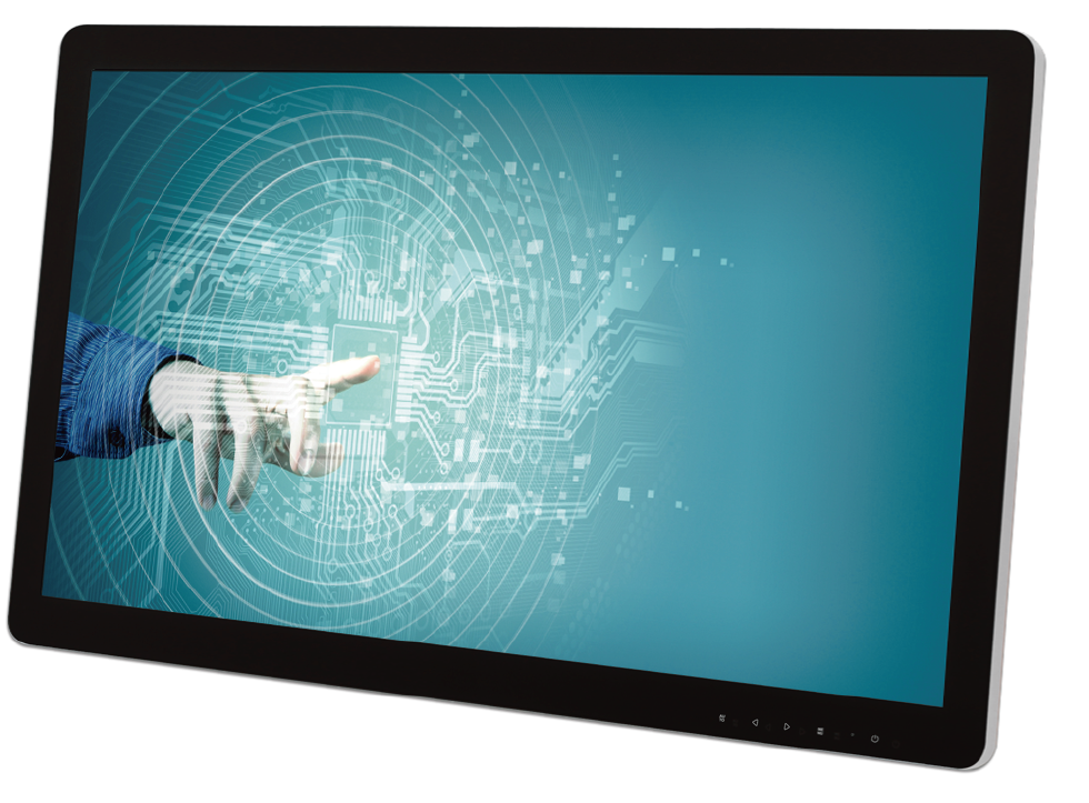
American Portwell Technology, Inc., (https://www.portwell.com), a world-leading innovator in Industrial PC (IPC) and an Associate member of the Intel® Internet of Things (IoT) Alliance, announces the LEAD-PD, -PND and -PPC series, a new family of panel PC products designed for the IoT market as a robust, functional and flexible multi-touch human machine interface (HMI). According to Jack Lam, American Portwell Technology’s product marketing director, the new LEAD series provides a rich portfolio of touch displays or fanless panel PCs with a variety of connectivity and computing flexibility. “Besides the option of two sizes and two colors,” Lam confirms, “the new LEAD series features full HD 10-point projective capacitive touch screen with stylish, slim and bezel-free outlook. Plus,” Lam adds, “a solid IP65 water- and dust-proof front panel, and fast time to market”.
Lam suggests applications for Portwell’s LEAD series include smart hospital/healthcare, such as information terminal, bedside infotainment, telemedicine and self-check system. Smart retail applications include digital signage, recognition, customized advertisements/ promotions, merchandise locations, self-checkout and delivery. Kiosk applications include point of interest, point of information in hospitality locations such as hotel or restaurant; transportation such as parking lot, train station, airport; library, exhibition hall; government infrastructure; industrial/factory automation; facility management; intralogistics or smart warehouse and much more.
LEAD Series: Common Features
“The LEAD series currently consists of three subsets” explains Maria Yang, American Portwell’s product marketing engineer. “LEAD-PD series, a Touch Display with multi-touch function; LEAD-PND series, an ARM-based flat panel PC that supports Android™ operating system with wireless connectivity; and LEAD-PPC series, utilizing Intel Atom® Dual Core® processor compatible with Win 10 IoT, Linux and Android operating system.”
According to Yang, all three models share the following common features: display sizes of 21.5˝ or 23.6˝; back shell colors in black or white—the white shell made of medical-grade, flame-retardant plastics; full HD 1920 x 1080 resolution wide-screen display; 16:9 ration panel; P-CAP and 10-point multi-touch glove operation; fanless, stylish and bezel-free design, suitable to face end users; standalone or VESA® 75mm x 75mm mounting options; ingress protection rating of IP65 water- and dust-proof front panel; certified to CE (EN 55032 and EN 55024), FCC 47CFR Part 15 Subpart B and EN 60068-2-6 for vibration and shock absorption.
Zooming, Rotating, Panning and More
“Portwell LEAD series’ 10-point multi-touch display supports a full set of gestures such as zooming in and out,” says Yang, “as well as panning or rotating. This gives users a whole new way to control and interact with what’s on the screen, even while wearing surgical or thin cotton gloves. And,” she adds, “the VESA mounting can support both portrait and landscape modes.”
Convenient, Versatile and Future-Proof for IoT
“We envisage our customers using the LEAD series as an add-on product to supplement Portwell’s industrial or embedded computers,” says Jack Lam. “It’s convenient and easy to use and will expedite time-to-market for their own products. Because it is fanless, with a slim and stylish bezel-free design, the new LEAD series makes it ideal for facing end users. Plus,” he adds, “the features such as the P-CAP multi-touch, IP65 water- and dust-proof front panel and flexible choice of connectivity enables this product to function in multiple environments. And as always,” Lam confirms, “our customers not only benefit from the most up-to-date technology and features, but they also gain peace of mind from the long lifespan support inherent with every Portwell product.”
For more information on other members of this family, see EDITOR’S NOTES at the end of this release or check this page.
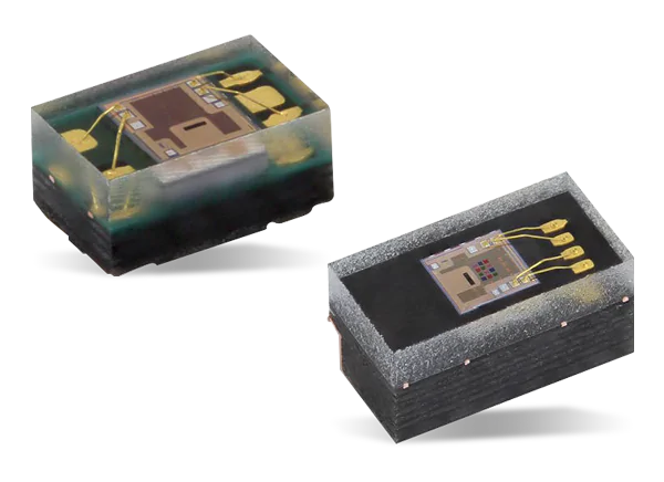
Vishay Intertechnology, Inc.today broadens its optoelectronics portfolio with new RGBC-IR sensors for applications such as automatic white balancing and color cast correction in digital cameras; automatic LCD backlight adjustment; and active monitoring of LED color output for IoT and smart lighting. The new VEML3328 (top-looking) and VEML3328SL (side-looking) sensors offer better linearity and higher sensitivity compared to previous generation devices, as well as new features including an infrared (IR) channel.
The sensors released today sense red, green, blue, clear, and IR light by incorporating photodiodes, amplifiers, and analog / digital circuits into a single CMOS chip. With the ability to calculate color temperature and sense ambient light, the devices offer a compact solution for adjusting backlighting in consumer electronics and notebook computers. They can also help to differentiate indoor from outdoor lighting environments to ensure that displays maintain consistent true color and ideal brightness levels based on the current environment lighting conditions.
In addition to digital camera and TV applications, the VEML3328 and VEML3328SL will also be used in various industrial and consumer applications where their excellent temperature compensation capability will keep the sensors’ output stable under changing temperatures.
The sensors’ built-in ambient light photodiode offers extremely high sensitivity, allowing the devices to operate in applications with dark lens designs. A programmable analog gain and integration time function, as well as the additional IR channel, allow designers to tailor the VEML3328 and VEML3328SL to their applications.
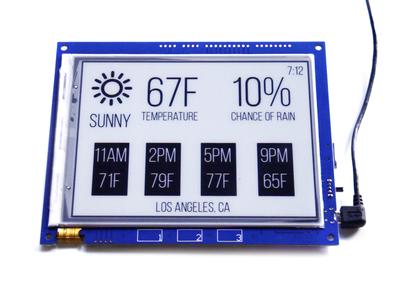
If you have ever wondered if there could be a better use for old Kindle screens, then you have to check out the new e-paper display made by e-radionica. The Inkplate 6 is made from recycled Amazon kindle screens. E-paper or electronic paper is an invention which has provided a solution to a pressing problem; blue light. E-papers solve this problem by reflecting light instead of emitting it. The team, therefore, decided to reform this technology, and Inkplate 6 is the result of that decision.
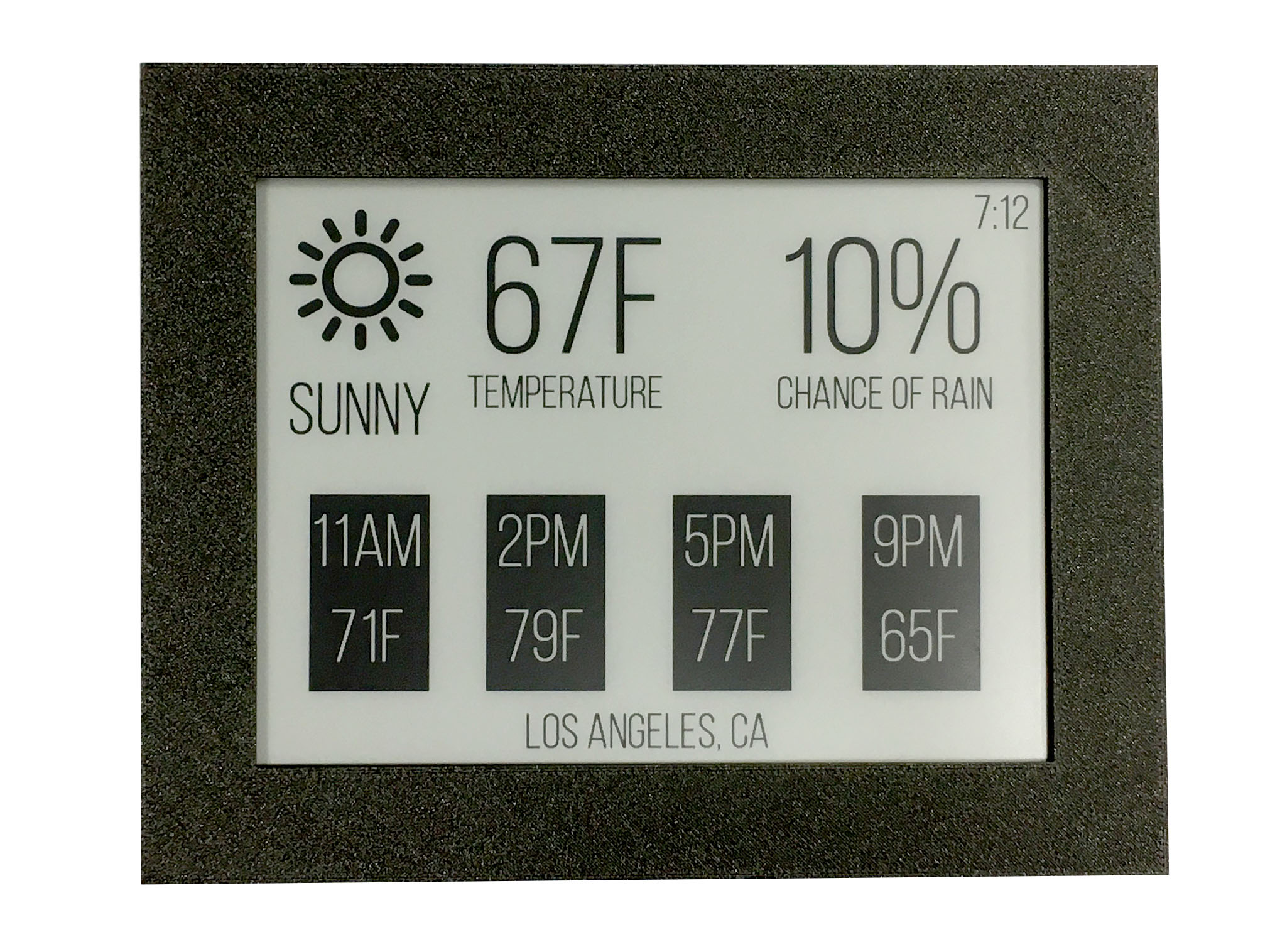
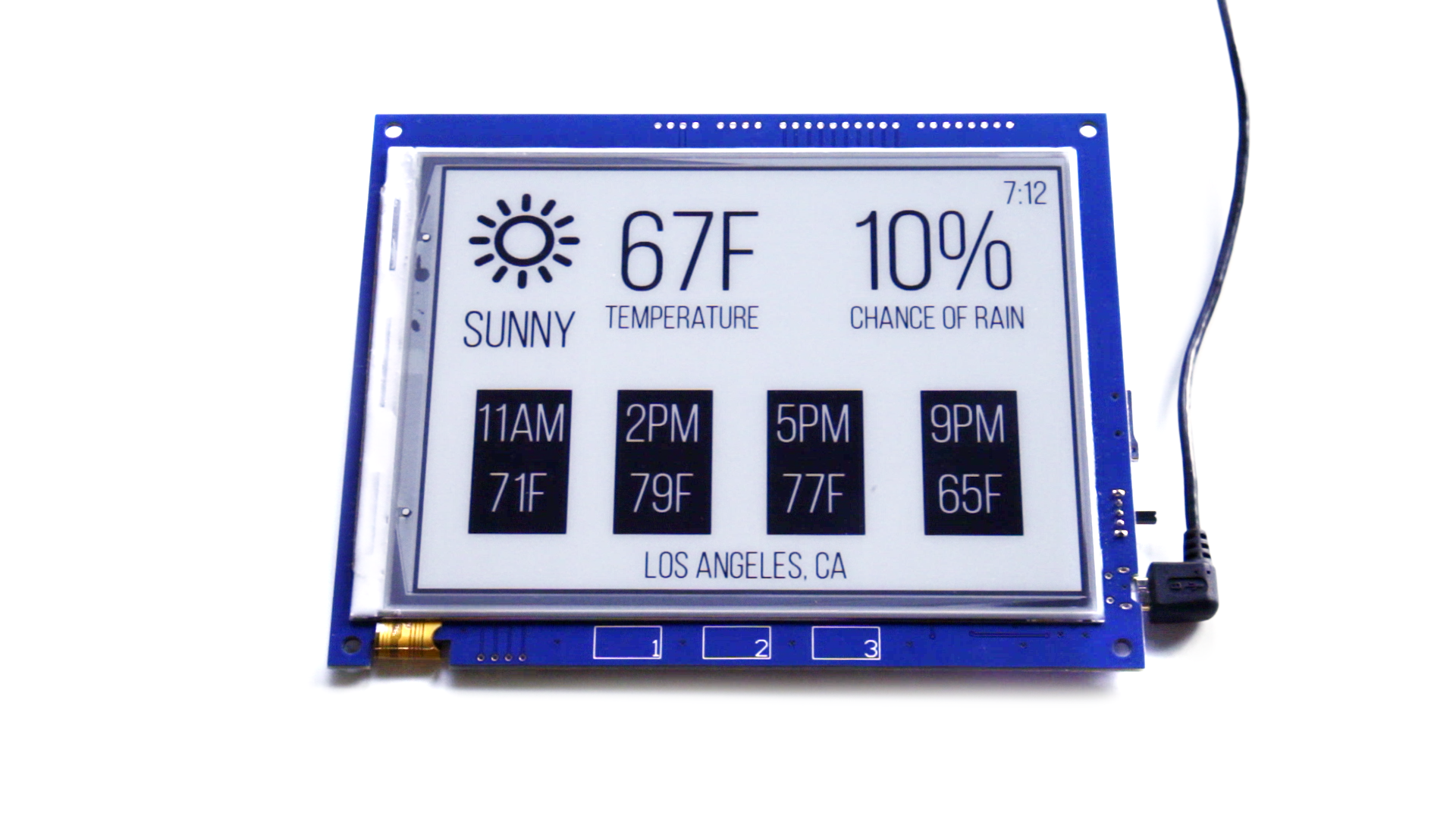
Inkplate 6 is a Versatile, easy-to-use, Wi-Fi-enabled e-paper display.
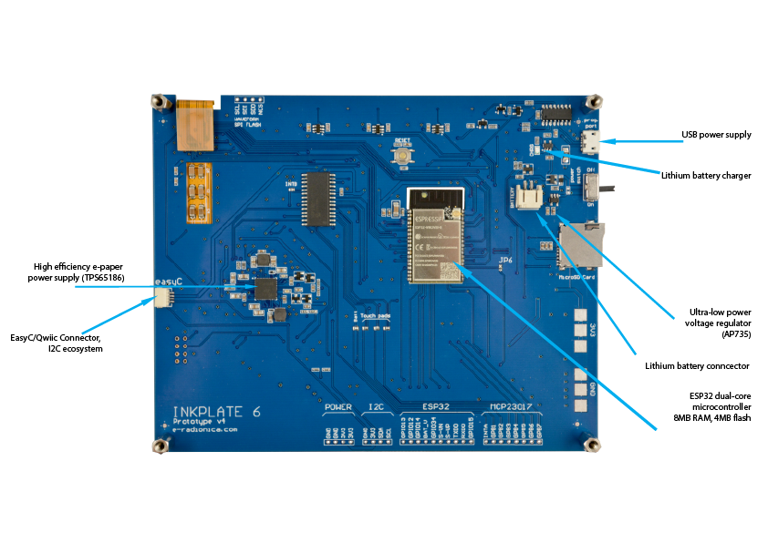
Inkplate 6 is built on the ESP32 WROOM microprocessor – a low power System on Chip (SoC) – which has Wi-Fi integrated and Bluetooth Low Energy (BLE) connectivity. Therefore, users can reprogram the screen content to display what they want which can be achieved using their Arduino library, which is completely compatible with Adafruit GFX or the Micro-python module provided.
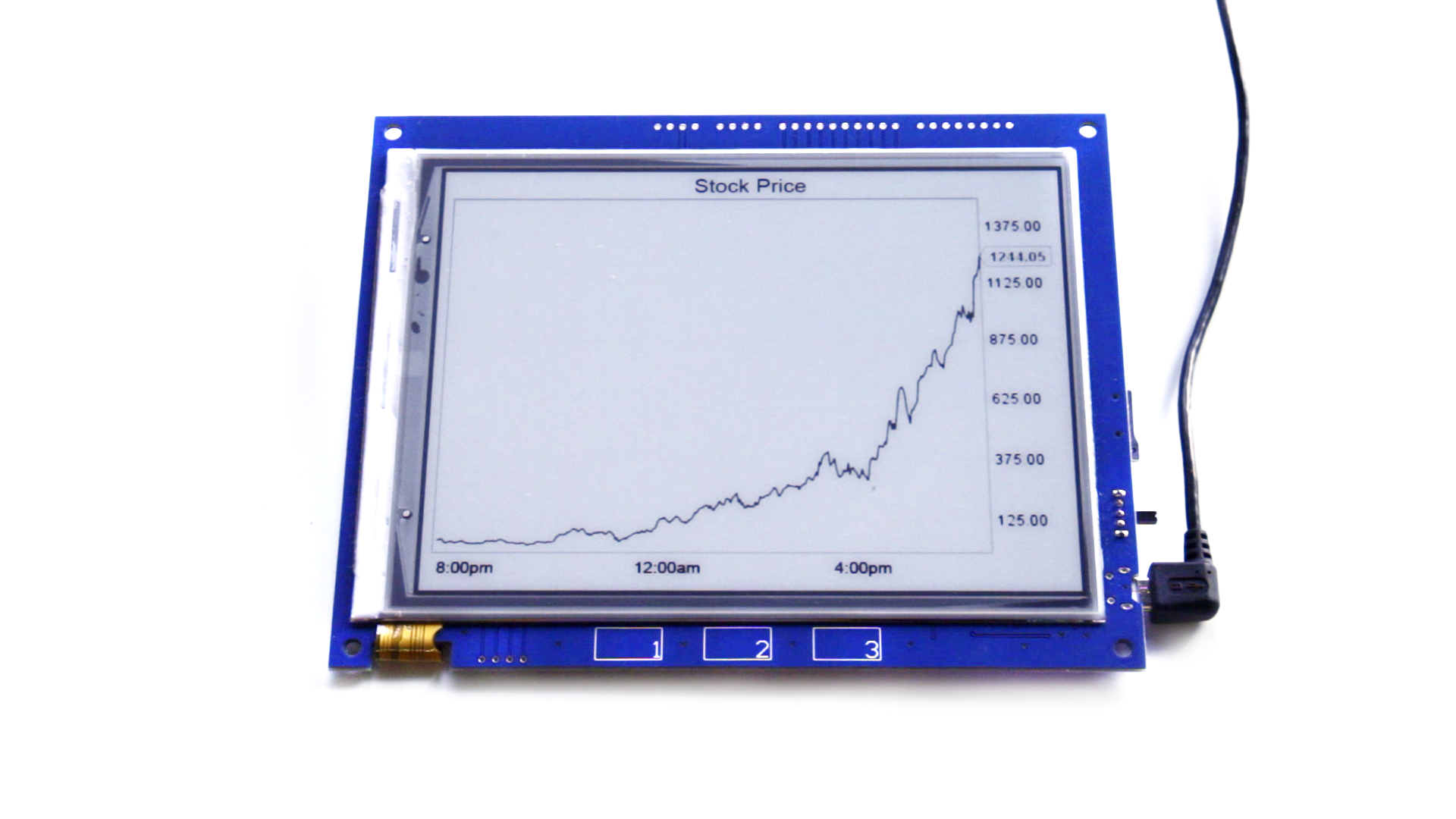
The 6-inch e-paper has an 800 x 600pixel resolution. It comes with a greyscale mode and black and white, like regular ink on a paper. The Inkplate comes with a microSD card slot so that images can be uploaded to the device. Partial updates are accepted, and this is fantastic because users do not have to change the entire screen when adding new content.
There are so many things that can be done with Inkplate 6. One can use it as a To-Do list for tasks or even a grocery list. It can also act as a collection of different online newspapers a user reads. The display content is totally up to the user.
Some of the device specifications are:
A 250 ms screen refresh time.
EasyC or Qwiic connector with I2C.
Headers for power signals, I2C, SPI, ESP32’s GPIO, and an MCP23017 I2C I/O expander
Internal TPS65186 temperature sensor
Hardware reset button
MCP73831 lithium battery charger with a standard JST connector
Power: 5V via micro USB port, or LiPo battery
Furthermore, there are three capacitive touchpads on the bottom of the device which serve as a source of input and one LED battery indicator. GPIO pins are also available and a Micro USB port for power and data. This open firmware device also comes with 8MP of RAM and 4MB of flash storage. Another amazing feature is good battery life. Since it has a 25 µA current in sleep mode, the device can be used for weeks after a single charge.
Inkplate 6, which launched a Crowd Supply campaign, has already surpassed the $10,000 goal they had. All documentation for the device can be found on Github. The device costs $99 and comes with free shipping to the U.S. Consumers from other countries must pay a $10 shipping fee. Users should expect delivery of the first batch of the device in April 2020
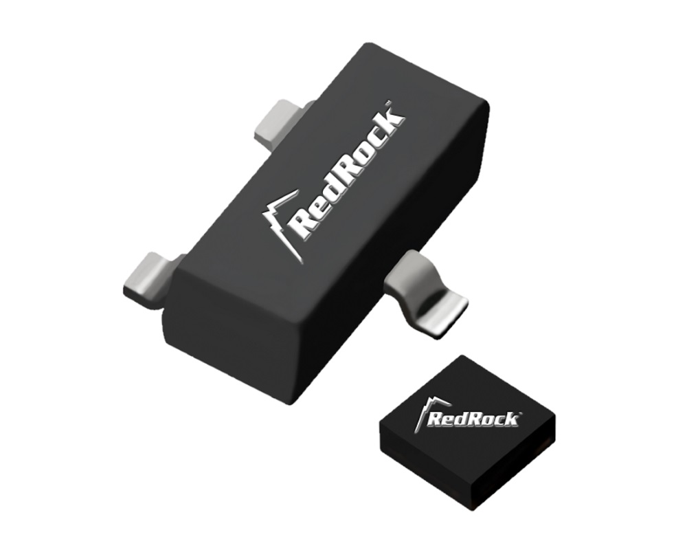
The RedRock™ RR121-1A53-311 is a magnetic sensor with a digital logic output from Coto. It features available operate sensitivity of 9G with an omnipolar magnetic field response all with a supply voltage of 3Vdd(typical), an average supply current drain of 1.44µA, as well as a high operating temperature from −40°C up to +125°C. The RedRock™ RR121 series is ideal for use in medical, industrial, automotive, and consumer applications. Based on patented Tunneling Magnetoresistance (TMR) technology with seamless CMOS integration, the RR121 series offers multiple configurations of several parameters to enable applications like proximity sensing, rotary sensing, and level detection.
Features
Magnetic sensor with digital logic output
Operate sensitivity of 9G (typically)
Release sensitivity of 5G (typically)
Hysteresis (BHYST) 4 (typically)
Frequency of 250Hz
Temperature range of -40° to +125°
Average supply current (Iavg) 1.44µA
Supply voltage 3Vdd (typically)
SOT-23-3 package
Omnipolar magnetic polarity response
RoHS and REACH compliant
Based on patented Tunnelling Magnetoresistance (TMR) technology with seamless CMOS integration, the RR121 series offers multiple configurations or several parameters to enable applications like:
Proximity detection
Rotary sensing
Motor controllers
Fluid level detection
Utility meters
Consumer electronics
Door and lid closure detection
Portable medical devices
Wake-up microprocessor
For further information on the RedRock RR121 Series, please click here.
For further information on the complete Redrock range please click here.
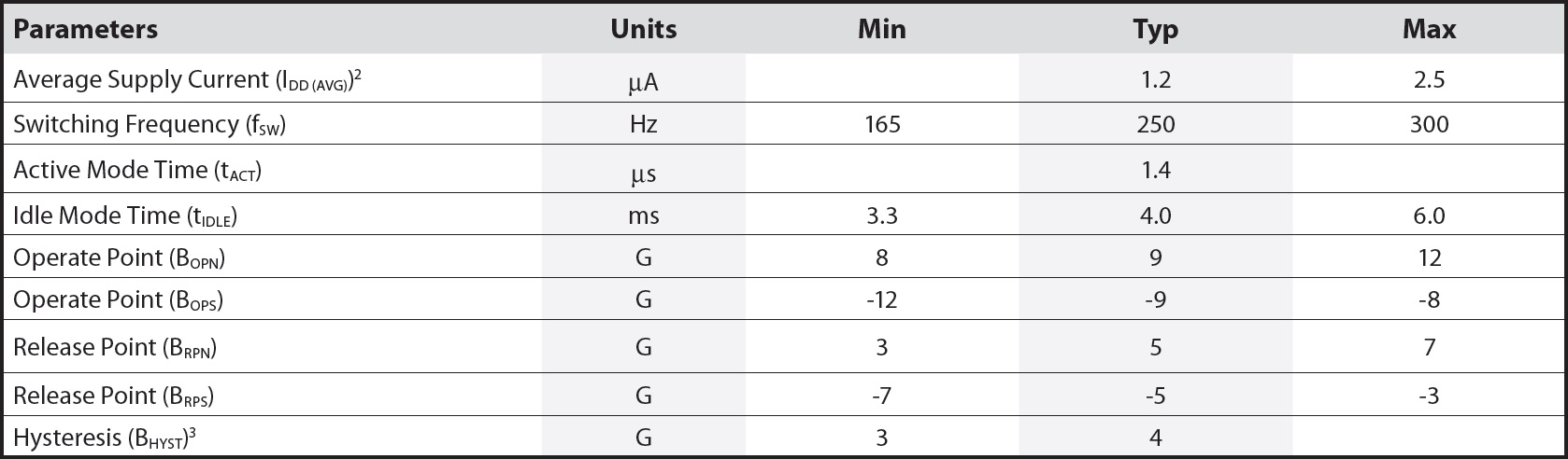
Being able to turn a USB-C supply to a variable power supply is certainly a big deal for a simple ingenious board like the ZY12PDN board shared by Keneth Finnegan on his twitter handle recently. The ZY12PDN is a simple STM-powered adapter board that turns a USB-C supply to a universal power supply for almost any electronic device.
We know that a USB-C, when it comes to power delivery, allows you to negotiate for 5, 9, 12, 15, 20 volts, with supply up to 100W which makes it possible to charge devices like laptops, phones, tablets, but the simplicity with which the ZY12PDN achieves it, brings lot of possibilities to the table.
The ZY12PDN, a USB-C power delivery trigger board uses the USB-C power delivery protocols to negotiate the level of voltage you want. The ZY12PDN has an STM32 microcontroller that helps in negotiating for the PD protocol. It also has, on one of its sides, a USB-C connector and on another side, header pins, USB-A connector and landing patterns for screw terminals.
Unlike some other USB power delivery adapters that need I2C communication for configuration, this power adapter board makes use of a push-button for setting the voltage you want to negotiate. “Finnegan” has created a video, that shows how the device works since the board does not come with any instructions. He explained that the board must first be configured anytime it is powered up with a sequence that helps to program the board, forcing it to stay powered-up in the desired mode. When connected, the USB power delivery uses a separate communication channel that automatically determines which becomes the supply and which the sink after which they negotiate the power profile they want to use in terms of voltage and current limits.
Some specifications of the board include:
Voltage: 3 – 20 volts
Current: 0 – 5A
Power: 100W
Weight: 0.8 ounces
Dimensions: 6.7 X 5.2 X 0.3 inches
The board is currently being sold alongside a decoy fast charge trigger detector on Amazon for $15.99, or eBay.com or Aliexpress.com. While technical information available for the board is limited, more details about the board can be gleaned from Kenneth’s video above.
Smaller is better when it comes to microchips, researchers said, and by using 3D components on a standardized 2D microchip manufacturing platform, developers can use up to 100 times less chip space. A team of engineers has boosted the performance of its previously developed 3D inductor technology by adding as much as three orders of magnitudes more induction to meet the performance demands of modern electronic devices.
In a study led by Xiuling Li, an electrical and computer engineering professor at the University of Illinois and interim director of the Holonyak Micro and Nanotechnology Laboratory, engineers introduce a microchip inductor capable of tens of millitesla-level magnetic induction. Using fully integrated, self-rolling magnetic nanoparticle-filled tubes, the technology ensures a condensed magnetic field distribution and energy storage in 3D space – all while keeping the tiny footprint needed to fit on a chip. The findings of the study are published in the journal Science Advances.
Traditional microchip inductors are relatively large 2D spirals of wire, with each turn of the wire producing stronger inductance. In a previous study, Li’s research group developed 3D inductors using 2D processing by switching to a rolled membrane paradigm, which allows for wire spiraling out of plane and is separated by an insulating thin film from turn to turn. When unrolled, the previous wire membranes were 1 millimeter long but took up 100 times less space than the traditional 2D inductors. The wire membranes reported in this work are 10 times the length at 1 centimeter, allowing for even more turns – and higher inductance – while taking up about the same amount of chip space.
“A longer membrane means more unruly rolling if not controlled,” Li said. “Previously, the self-rolling process was triggered and took place in a liquid solution. However, we found that while working with longer membranes, allowing the process to occur in a vapor phase gave us much better control to form tighter, more even rolls.”
Another key development in the new microchip inductors is the addition of a solid iron core.
“The most efficient inductors are typically an iron core wrapped with metal wire, which works well in electronic circuits where size is not as important of a consideration,” Li said. “But that does not work at the microchip level, nor is it conducive to the self-rolling process, so we needed to find a different way.”
To do this, the researchers filled the already-rolled membranes with an iron oxide nanoparticle solution using a tiny dropper.
“We take advantage of capillary pressure, which sucks droplets of the solution into the cores,” Li said. “The solution dries, leaving iron deposited inside the tube. This adds properties that are favorable compared to industry-standard solid cores, allowing these devices to operate at higher frequency with less performance loss.”
Though a significant advance on earlier technology, the new microchip inductors still have a variety of issues that the team is addressing, Li said.
“As with any miniaturized electronic device, the grand challenge is heat dissipation,” she said. “We are addressing this by working with collaborators to find materials that are better at dissipating the heat generated during induction. If properly addressed, the magnetic induction of these devices could be as large as hundreds to thousands of millitesla, making them useful in a wide range of applications including power electronics, magnetic resonance imaging and communications.”
Researchers from Stanford University, Hefei University of Technology, China, and the University of Twente, The Netherlands also participated in this study.
The National Science Foundation Engineering Research Center for Power Optimization of Electro-Thermal Systems and the U.S. Department of Energy supported this research.
The paper “Monolithic mtesla-level magnetic induction by self-rolled-up membrane technology” is available online and from the U. of I. News Bureau. DOI: 10.1126/sciadv.aay4508
A while back, I noticed an ESP32 based Camera board called the ESP32-CAM on LCSC.com, and planned on getting one to play with but didn’t get the chance until recently when I saw a tutorial by Rui Santos based on the board. I feel its a nice board and today’s tutorial will focus on building a Video Streaming Server using the ESP32-CAM board.
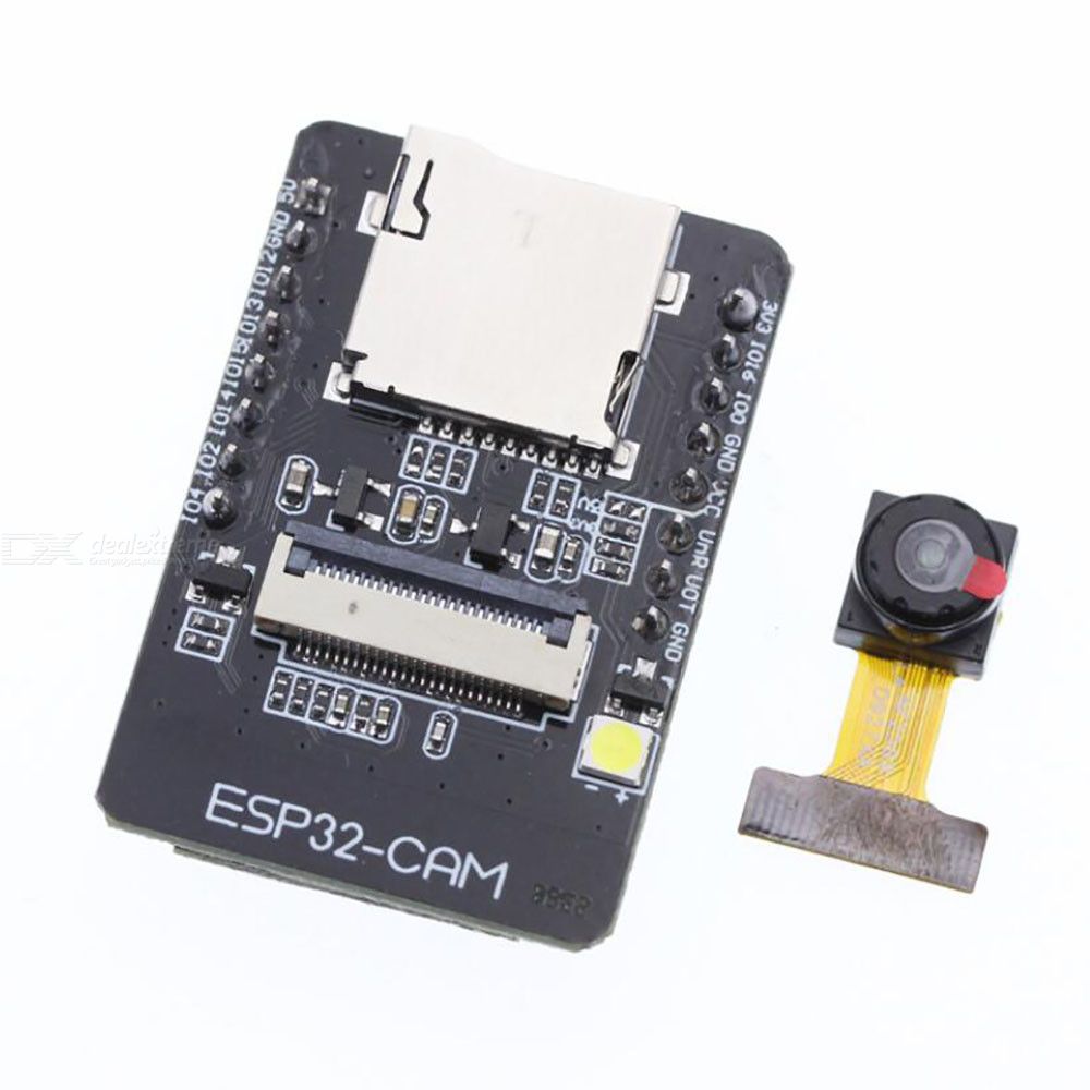
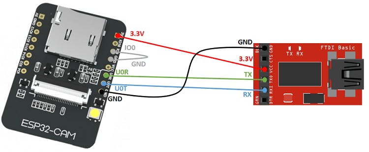
The ESP32-CAM is very cheap (costs less than $10), a small camera module, based on the ESP32-S chip from AI-thinker. It essentially comprises an OV2640 camera embedded with an ESP32 module with several GPIOs to which peripherals (sensors and actuators) can be connected, and a microSD card slot which could be useful in storing images from the camera. Highlighting the fact that it was designed for stand-alone camera-based applications only, the ESP32-CAM doesn’t come with features like a USB port, etc, all of which are available on regular ESP-32 boards. The lack of USB ports also means the lack of an FTDI chip as such, to program the board, you will need to use an FTDI Programmer.
ESP32-CAM (source: Dealextreme)
Some of the features of the ESP32-CAM board are highlighted below:
802.11b/g/n Wi-Fi BT SoC module with support for STA/AP/STA+AP operation mode
Low power 32-bit CPU, can also serve the application processor
Up to 160MHz clock speed, summary computing power up to 600 DMIPS
Built-in 520 KB SRAM, external 4MPSRAM
Supports UART/SPI/I2C/PWM/ADC/DAC
Support OV2640 and OV7670 cameras, and has a built-in flash lamp
Support image WiFI upload
SD card Slot
Embedded Lwip and FreeRTOS
Support Smart Config/AirKiss technology
Support for serial port local and remote firmware upgrades (FOTA)
To demonstrate how the ESP32-CAM works, we are going to build a Video Streaming Server whose IP address can be accessed from outside to get a live stream from the ESP32-CAM Camera.
The steps are quite easy and at the end of the tutorial, you should be familiar with the ESP32-CAM, enough to build a more astounding project with it.
The components can be bought from the attached links. For the FTDI, the SparkFun’s FTDI Basic Breakout was used but you can decide to use any other similar board with 3.3V logic level.
Schematics
The ESP32-CAM comes with the camera connected, and if this is different in your case, all you need do is connect the camera to the port provided. This leaves us with the connection between the ESP32-CAM and the FTDI Programmer. The FTDI programmer communicates with the ESP32-CAM over UART as such, it will be connected to the UART pin of the ESP32-CAM. The connection is illustrated in the schematics below;
Go over the connection once more to ensure everything is as it should be.
CODE
We will use the Arduino IDE for this project, as such, there is a need for us to set up the Arduino IDE with the board files for the ESP32. Follow the steps detailed in this tutorial we wrote a while back on “Programming the ESP32 with the Arduino IDE” to get it done.
The code for today’s project is based on the CameraWebserver example in the ESP32 Library. The idea behind the project is simple, the ESP32-CAM board is configured as a web server, serving live feed from the camera on a webpage, so any browser on the same network as the ESP can view the live feed by going to the board’s IP address.
The code uses the esp_camera library along with the WiFi.h library. The esp_Camera library contains functions that grant access to the camera and functions to take pictures and record videos among other things, while the ESP’s WiFi.h library comprises functions that allow us to set up the ESP32 as a web server among other things. These libraries are installed when you install the ESP32 Arduino IDE add-on, as such, they require no special installation process.
As usual, I will do a quick explanation of some parts of the code and provide the complete code at the end of the project.
The code starts with the inclusion of all the libraries that we will use. Depending on your version of the ESP32 library/add-on, the Camera_pins.h file will either be attached as a file to the sketch or it’s content copied into the sketch. In our case, it was attached as a file, and the file has been added to the files under the download section.
Next is the void setup() function. We start the function by initializing serial communication, after which we configure the camera, setting its pins to that of the variables stored in the Camera_pins.h file. We also set things like its frequency and pixel format among others.
Next, we initialize the camera using the configurations created
// camera init
esp_err_t err = esp_camera_init(&config);
if (err != ESP_OK) {
Serial.printf("Camera init failed with error 0x%x", err);
return;
}
and set the properties of the camera sensor being used.
sensor_t * s = esp_camera_sensor_get();
//initial sensors are flipped vertically and colors are a bit saturated
if (s->id.PID == OV3660_PID) {
s->set_vflip(s, 1);//flip it back
s->set_brightness(s, 1);//up the blightness just a bit
s->set_saturation(s, -2);//lower the saturation
}
//drop down frame size for higher initial frame rate
s->set_framesize(s, FRAMESIZE_QVGA);
#if defined(CAMERA_MODEL_M5STACK_WIDE)
s->set_vflip(s, 1);
s->set_hmirror(s, 1);
#endif
Next, we connect the node to the access point using the credentials provided earlier and verify the connection status.
With the WiFi connected, we call the StartCameraServer() function which automatically begins streaming the camera feed to a webpage that can be accessed via the IP address of the board (displayed on the serial monitor using the Wifi.localIP()) function).
startCameraServer();
Serial.print("Camera Ready! Use 'http://");
Serial.print(WiFi.localIP());
Serial.println("' to connect");
}
The void loop() function just introduces a delay at every refresh point.
The StartCameraServer() function is one of the functions built into the ESP32 library. You can check it out to better understand how it works.
The complete code for the project is provided below and also attached under the download section.
#include "esp_camera.h"
#include <WiFi.h>
#include "camera_pins.h"
//
// WARNING!!! Make sure that you have either selected ESP32 Wrover Module,
// or another board which has PSRAM enabled
//
// Select camera model
//#define CAMERA_MODEL_WROVER_KIT
//#define CAMERA_MODEL_ESP_EYE
//#define CAMERA_MODEL_M5STACK_PSRAM
//#define CAMERA_MODEL_M5STACK_WIDE
#define CAMERA_MODEL_AI_THINKER
const char* ssid = "ssid";
const char* password = "password";

void startCameraServer();
void setup() {
Serial.begin(115200);
Serial.setDebugOutput(true);
Serial.println();
camera_config_t config;
  config.ledc_channel = LEDC_CHANNEL_0;
  config.ledc_timer = LEDC_TIMER_0;
  config.pin_d0 = Y2_GPIO_NUM;
  config.pin_d1 = Y3_GPIO_NUM;
  config.pin_d2 = Y4_GPIO_NUM;
  config.pin_d3 = Y5_GPIO_NUM;
  config.pin_d4 = Y6_GPIO_NUM;
  config.pin_d5 = Y7_GPIO_NUM;
  config.pin_d6 = Y8_GPIO_NUM;
  config.pin_d7 = Y9_GPIO_NUM;
  config.pin_xclk = XCLK_GPIO_NUM;
  config.pin_pclk = PCLK_GPIO_NUM;
  config.pin_vsync = VSYNC_GPIO_NUM;
  config.pin_href = HREF_GPIO_NUM;
  config.pin_sscb_sda = SIOD_GPIO_NUM;
  config.pin_sscb_scl = SIOC_GPIO_NUM;
  config.pin_pwdn = PWDN_GPIO_NUM;
  config.pin_reset = RESET_GPIO_NUM;
  config.xclk_freq_hz = 20000000;
  config.pixel_format = PIXFORMAT_JPEG;
//init with high specs to pre-allocate larger buffers
if(psramFound()){
   config.frame_size = FRAMESIZE_UXGA;
   config.jpeg_quality = 10;
   config.fb_count = 2;
 } else {
   config.frame_size = FRAMESIZE_SVGA;
   config.jpeg_quality = 12;
   config.fb_count = 1;
 }
#if defined(CAMERA_MODEL_ESP_EYE)
pinMode(13, INPUT_PULLUP);
pinMode(14, INPUT_PULLUP);
#endif
// camera init
esp_err_t err = esp_camera_init(&config);
if (err != ESP_OK) {
  Serial.printf("Camera init failed with error 0x%x", err);
  return;
}
  sensor_t * s = esp_camera_sensor_get();
  //initial sensors are flipped vertically and colors are a bit saturated
  if (s->id.PID == OV3660_PID) {
    s->set_vflip(s, 1);//flip it back
    s->set_brightness(s, 1);//up the blightness just a bit
    s->set_saturation(s, -2);//lower the saturation
  }
  //drop down frame size for higher initial frame rate
  s->set_framesize(s, FRAMESIZE_QVGA);

#if defined(CAMERA_MODEL_M5STACK_WIDE)
  s->set_vflip(s, 1);
  s->set_hmirror(s, 1);
#endif
WiFi.begin(ssid, password);

 while (WiFi.status() != WL_CONNECTED) {
   delay(500);
   Serial.print(".");
 }
 Serial.println("");
 Serial.println("WiFi connected");
 startCameraServer();

  Serial.print("Camera Ready! Use 'http://");
  Serial.print(WiFi.localIP());
  Serial.println("' to connect");
}
void loop() {
// put your main code here, to run repeatedly:
delay(10000);
}
Demo
With the ESP-32 CAM connected to the FTDI programmer, ensure the GPIO O pin is connected to GND, then connect the programmer to your PC and follow this next steps to upload the code:
Go to Tools > Board and select ESP32 Wrover Module
Go to Tools > Port and select the COM port the ESP32/FTDI is connected to
In Tools > Partition Scheme, select “Huge APP (3MB No OTA)“
Press the ESP32-CAM on-board RESET button
Then, click the upload button to upload the code
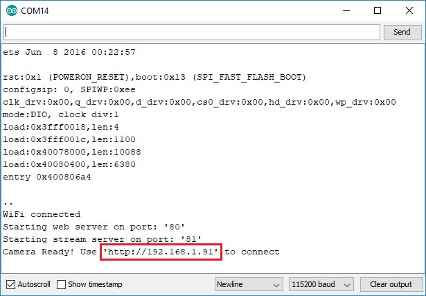
After uploading the code, disconnect GPIO 0 from GND and Open the Serial Monitor with the baud rate of 115200 (same as the serial.begin() function). Press the ESP32-CAM on-board Reset button, you should see the IP address of the ESP printed in the Serial Monitor as shown below.
IP address
To access the feeds from the camera, open a browser on a device on the same network as the ESP, and enter the ESP32-CAM IP address into the address bar. Press the Start Streaming button on the resulting page and you should see the video being streamed.
Quite a number of advancements can be made to the project. With little or no additional coding, you can easily connect the project to your home assistant, so you can view the stream from the Home Assistant app and with a little more effort and an SD Card, we can take this do things like facial recognition.
That’s it! Feel free to reach me via the comment section with questions about the project and also let me know if you will be making any improvements to it.
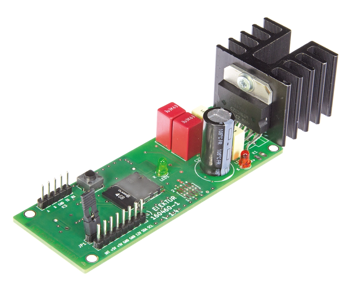
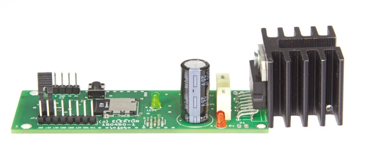
With a smartphone or an MP3 player it’s easy to play audio files, but generally not at room strength or if you can, only in wretched quality. The Card Sound project makes it possible to fill the room with music and have excellent sound reproduction! This lightweight and compact player also stands out for its modest quiescent current consumption and desirable extra features such as I²C and RS-485 control.
Quick Features:
Analogue/digital supply voltages: 3 to 18 VDC / 4.5 to 12 VDC
Analogue/digital current requirements: see Measurements panel
Sinewave output power Pout into 4 or 8 Ohm: 12.5 W or 6.25 W (measured at 10.0 V peak-to-peak)
Output: short-circuit protected max. 2 A
Harmonic distortion: see Measurements panel
Zero-value noise: around 1.4 mW
Data formats: PCM 16, 24, 32-bit for each of 32, 44.1, 48, 96, 128 kHz Stereo
Dimensions (L x W x H): 89 x 33 x 30 mm
Weight without SD card: 26 g
Figures valid with a supply voltage of 5 VDC (digital) and 12 VDC (analogue) for a 1 kHz sinewave signal with 16 bits and 44.1 kHz sampling rate
Article Details:
Original publication: Elektor magazine issue 1/2018 on page 44.
Author: Falko Bilz
Free download expires: Friday 31 January, 2019.
Original article production number: 160460
PCB available: yes, see Products below
Like what you’re seeing? Then go to the article page and download a pdf copy of the full, original article. Downloading is free from Friday 24 January to Friday 31 January 2020.
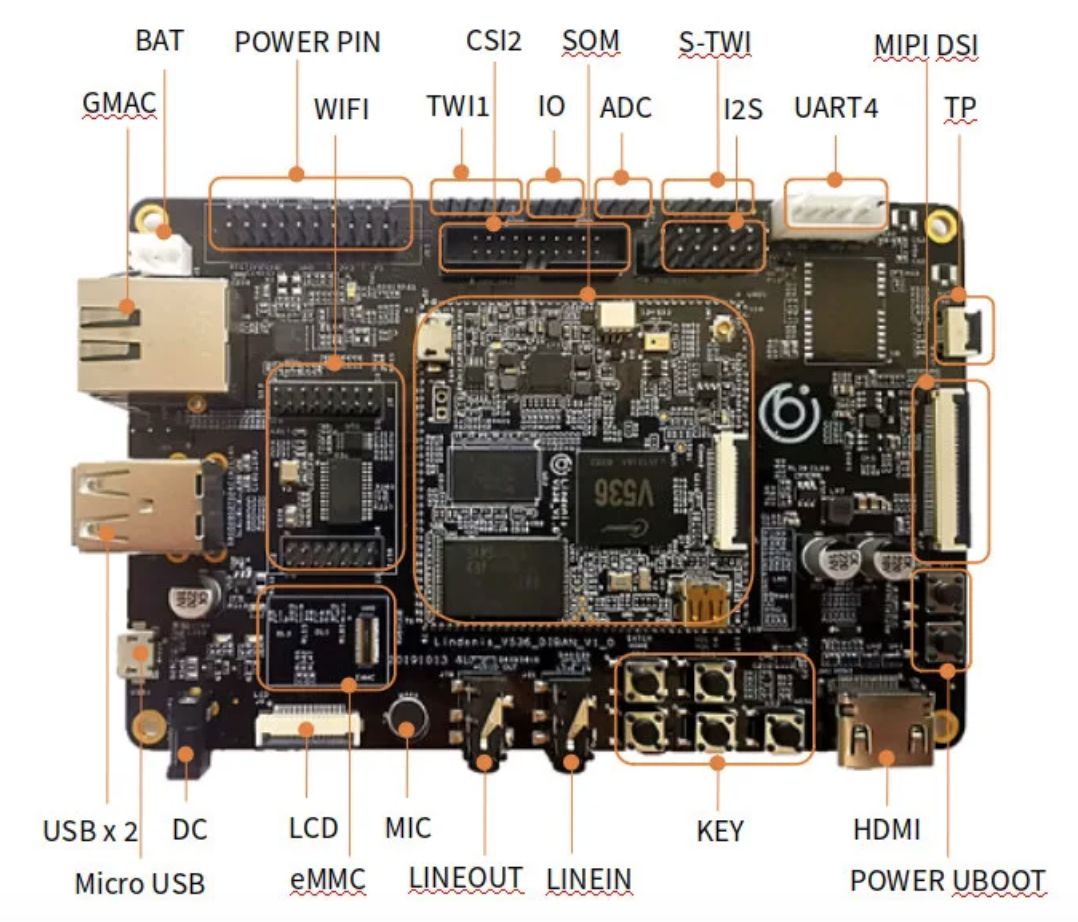
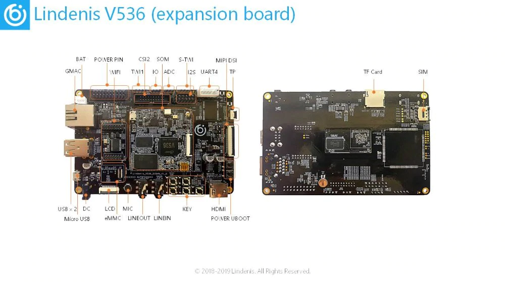
Similar to the earlier Lindenis V5 designed for AI video processing and 4K encoding, Lindenis has released another single-board computer that uses SoM and baseboard design for 4K camera applications called the Lindenis V536.
The Lindenis V536 which runs on a new Allwinner dual Cortex-A7 processor and a single MIPI SCI interface was designed for applications that rely heavily on popular open-source packages such as Live555, V4L2, FFmpeg and custom framework, and libraries. Capable of doing a lot on image signal processing and video encoding/decoding functions, the Lindenis V536 is suitable for sample applications like 4K camera applications, media player applications, and low-latency A/V streaming applications. It supports functions like image mirroring and flipping, color enhancement and adjustment, bad pixel, and lens shading correction, providing ISP tools for the PC, contrast and sharpness enhancement, motion smear and color noise removal, real-time multi-stream encoding capability, eight ROI encoding as well as MJPEG / JPEG baseline encoding.
Hardware features and specifications include:
Expansion board
Dimension: 130 x 85mm
1 DVP connector for camera input
eMMC flash module connector and MicroSD card slot for storage
Analog microphone and 3.5mm line in and out jacks for audio
14-pin I2S header, 3-pin ADC header, 3-pin EINT – GPIO header and 4 –pin TWI header with 1 TWI and S-TWI each
Power supply – 5V/2A micro USB connector, 5V/2A via DC jack, 3.7V battery connector, and 20-pin power supply header
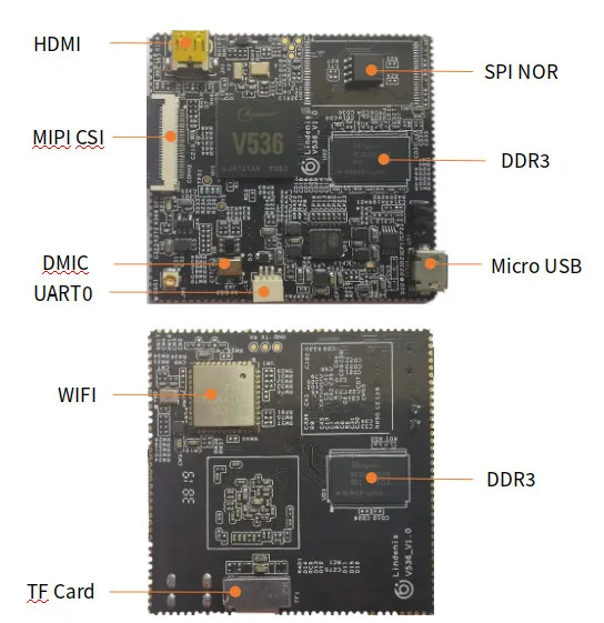
Core Board
50 x 50mm in size
1GB DDR3 for system memory
Allwinner V536 dual-core Cortex –A7 processor @ 1.2 GHz and 4K H.265/H.264 video decoding and encoding @30 fps, 28nm process
SPI NOR flash or SPI NAND flash, bootable MicroSD card for storage
MIPI CSI connector and MIPI HDMI 1.4 port for video input and output
Digital microphone for audio
802.11b/g/n/ac Wi-Fi 5 and Bluetooth 4.2 via AP6255 for connectivity
Baseboard Interface – Castellated holes
Power supply: 5V/2A via micro USB port or castellated holes
The Lindenis V536 also comes with an SDK that includes an OpenWrt with Linux 4.9, Arm GCC based cross-toolchain, U-Boot 2014.07 and an integrated build system. It is sold for a regular price of $52 while the SBC is sold for $94 together with other accessories like the HDMI cable, flash module, camera module, and Bluetooth/Wifi module.
More about the board and the SDK can be found on its wiki page.
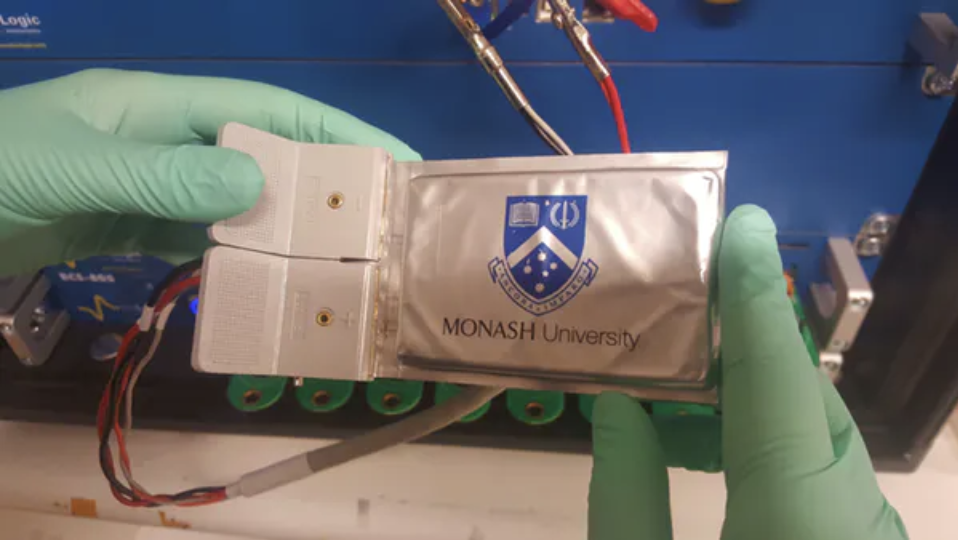
What would you give for a battery, 5x the storage capacity of whatever you’re reading from? Well, the countdown to commercial availability for batteries of this type of capacity has already begun and it would be considerably cheaper than then currently available batteries.
This radical improvement comes from using sulfur cathodes rather than graphite in lithium-ion batteries. Sulfur ranks high on the list of very abundant materials and is relatively cheap to produce unlike rare minerals like cobalt used to produce regular lithium-ion batteries. So why didn’t anyone think of this until now?
Actually, it’s pretty well known that lithium-sulfur batteries can store far more energy than their lithium-ion counterparts, six-times in theory. However, the battery’s performance degrades quite rapidly due to its high storage capacity (That’s six times the stress—pretty understandable), as the sulfur cathode is nearly double its usual size when the battery is fully charged which destroys electron paths in the binder across the electrodes. As a result of this, repeated charging and discharging lead to rapid deterioration of the batteries’ performance.
Solving this problem was the goal of a research team at Monash University led by Mahdokt Shaibani, and their efforts have led to the development of a new technique for processing lithium-sulfur batteries that allows them to undergo hundreds of charge-discharge cycles without breaking down. Attaining a level of stability that is already being considered as a huge breakthrough in battery technology.
The team’s technique involved tweaking the process of making lithium-ion batteries just a little differently so that the binder across the electrodes can accommodate the expansion of the sulfur electrodes. In an article published to explain their work, Mahdokt Shaibani said:
“To make sure our batteries would be easy and cheap to manufacture, we used the same material as a binder but processed it a little differently. The result is a web-like network of binder that holds particles together but also leaves plenty of space for the material to expand. These expansion-tolerant electrodes can efficiently accommodate cycling stresses, allowing the sulfur particles to live up to their full energy storage capacity.”
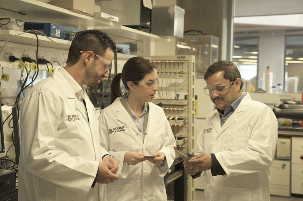
The Research Team (Credit: Monash University)
The approach adopted by the team not only favors high-performance long cycle life but also simplifies manufacturing and reduces associated cost, along with a significant reduction in hazardous waste thanks to the water-based nature of the process.
The research team includes Professor Mainak Majumder (Monash University), and Associate Professor Matthew Hill (CSIRO and Monash University) who is renowned for translating laboratory success to industrial application in record time, which is somewhat our hope for this breakthrough.
The study was published on Science Advances on Saturday, 4 January 2020. More information on the research can be obtained from the publication.