Isabellenhütte introduces new range of 1 – 6mΩ resistors in smallest chip sizes available on the market

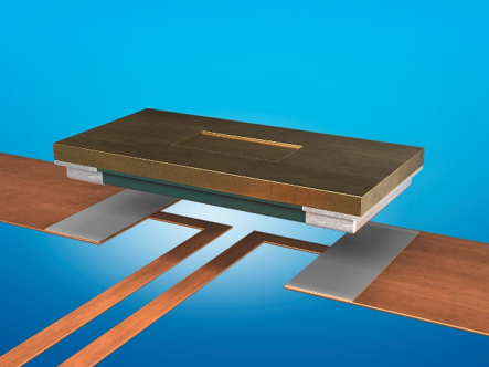
Isabellenhütte has developed a new range of precision resistors in standard sizes with resistances ranging from 1 to 6 mOhm for applications that require small and low-ohmic shunts. In terms of their construction, the components are also less complex than the current ISA-PLAN®resistance families. And yet, they offer the same performance quality: very good long-term stability, a low temperature coefficient, and low thermoelectric voltages.

With the FMx shunt family, Isabellenhütte has now plugged a gap in the standard size range for precision resistances. It has not been possible with the previous product ranges to realize the usual S (2512), P (2010) and K (1206) standard sizes in the resistance range from 5 to 1 mOhm. The impetus for this new development was provided by increasing demand for these resistances as well from a wide range of industries, including the automotive sector (for in-car chargers and assistance systems) and industry (for BLDC drive units), but also from the consumer market (e.g. for white goods).

The development approach

The large cross-sectional areas required for low-ohmic components have been achieved by a change in construction, and the production process has also been significantly simplified. A further milestone for the FMx shunts has been the development of the NOVENTIN® resistance alloy to make it possible to realize these low-ohmic values in defined sizes. Until now, the ISA-PLAN® resistances (SMx, VMx and CMx) have followed a sandwich construction, consisting of a substrate – usually copper – an adhesive and a resistance film made out of the ZERANIN® and MANGANIN® resistance alloys developed in-house by Isabellenhütte. The FM in the title of the new range stands for “Full Metal”, i.e. the components are fashioned in the corresponding thickness out of a full metal plate made of the resistance material in question and directly soldered onto the underside. These variant is very low-ohmic due to the large cross-sectional areas. 1 mOhm is realized with the ZERANIN® alloy, 2 mOhm with MANGANIN®, and, for the first time, NOVENTIN® is being used in ISA-PLAN® products for the resistance range from 3 to 6 mOhm. The new design has given rise to a particularly robust construction which also makes it possible to leave out some work stages and reduce costs. An important point for the automotive industry is this: The components form a soldering point meniscus to guarantee the possibility of automated inspection of the soldering points.

more information: www.isabellenhuette.de

NJR to Provide Samples of High Precision Adjustable Shunt Regulator NJM17431

NJR provides samples of a new adjustable shunt regulator NJM17431 with high precision and wide stable operation region that has been designed by latest process and analog circuit technology for many years.

Because the NJM17431 has 0.8% accurate voltage reference and wide stable operation region for large capacitive load, it can be used for a very wide range of applications. And it can replace Zener diode with the NJM17431.

Since the stable operation region is wide, it will help engineers reduce the design man-hours and the burden of replacement evaluation.

The NJM17431 operates stable in the range of 0.01 μF to 100 μF with the actual usage cathode current region.

Characteristics

  • Reference Voltage Tolerance: 2.5 V±0.8%
  • Adjustable Output Voltage: VREF to 36 V
  • Wide Stable Operation Region
  • Low Temperature Coefficient of Voltage Reference
  • The output voltage can be set with two external resistors
  • Bipolar Technology
  • Package: SOT-23-5

The part will enter mass-production in the second quarter of 2020. More information: www.njr.com

MP23ABS1TR – MEMS Audio Single Ended Microphone

The MP23ABS1 is a compact, low-power microphone built with a capacitive sensing element and an IC interface. The sensing element, capable of detecting acoustic waves, is manufactured using a specialized silicon micromachining process to produce audio sensors. The MP23ABS1 has an acoustic overload point of 130 dBSPL with a typical 64 dB signal-to-noise ratio. The sensitivity of the MP23ABS1 is -38 dBV ±1 dB @ 94 dBSPL, 1 kHz.

Features

  • Single supply voltage operation 1.52 V – 3.6 V
  • Omnidirectional sensitivity
  • High signal-to-noise ratio
  • High acoustic overload point: 130 dBSPL typ.
  • Package compliant with reflow soldering
  • Enhanced RF immunity
  • Ultra-flat frequency response
  • Low latency
  • Ultra-low-power: 150 μA max
  • ECOPACK®, RoHS, and “Green” compliant

Specifications

Be Heard

Dual Forward/Reverse DC Motor Driver with Brake for Robots

This high current forward-reverse DC motor driver is built using STK681-332 IC from ON Semiconductor. The circuit can drive brushed DC Motor with up to 12 A peak current. The circuit requires 3 input signals: Enable for PWM input for speed control, IN1 and IN2 to change the motor direction and to apply the brake while the motor is in running condition. Monitor (Fault) pin is used when either of the outputs short-circuits detector, overcurrent detector, or overheat detector is activated. When the detector is activated, this pin is set low and all outputs are latched off. If the output pin is short-circuited directly to VCC or connected directly to GND, an output short circuit condition is detected and the output is latched in the off state. To restart the operation, turn on 5V supply again. The maximum input frequency is 50 kHz. Both ICs required a large size heat sink to dissipate heat.

Dual Forward/Reverse DC Motor Driver with Brake for Robots – [Link]

Dual Forward/Reverse DC Motor Driver with Brake for Robots

This high current forward-reverse DC motor driver is built using STK681-332 IC from ON Semiconductor. The circuit can drive brushed DC Motor with up to 12 A peak current. The circuit requires 3 input signals: Enable for PWM input for speed control, IN1 and IN2 to change the motor direction and to apply the brake while the motor is in running condition. Monitor (Fault) pin is used when either of the outputs short-circuits detector, overcurrent detector, or overheat detector is activated. When the detector is activated, this pin is set low and all outputs are latched off. If the output pin is short-circuited directly to VCC or connected directly to GND, an output short circuit condition is detected and the output is latched in the off state. To restart the operation, turn on 5V supply again. The maximum input frequency is 50 kHz. Both ICs required a large size heat sink to dissipate heat.

Features:

  • DC Supply Input Up to 48V DC
  • Maximum Peak Current 12Amp
  • External current detection resistor allows overcurrent detection and peak current control in the PWM operation mode.
  • Maximum Operation Frequency 50Khz
  • Allows forward, reverse, and brake operations in accordance with the external input signal.
  • 12A peak startup output current and 12A peak brake output current.
  • On-chip outputs short-circuit detection function.

Schematic

Parts List

Connections

Timing Diagram

Truth Table

Photos

STK681-332 Datasheet

Multi-sensor SpO2 and Heart Rate Monitor (HRM) reference design with Bluetooth® 5

This reference design enables a wearable, optimized saturation of peripheral capillary oxygen (SpO2) and multi-sensor, multi-wavelength optical heart rate monitor (HRM). It uses AFE4420 device, which is a single-chip, bio-sensing front end for photoplethysmography (PPG) measurements. It supports up to four switching light-emitting diodes (LEDs) and up to four photodiodes to enable signal acquisition of up to 16 Phases. The CC2640R2F device (supporting Bluetooth® low energy 4.2 and 5) transfers the measured data to a remote location. This patient-monitoring design uses a single CR3032 battery with a 30-day life cycle. Raw data is available to calculate heart rate, SpO2, and other related parameters. 2 onboard light-emitting diodes (LEDs) identify low-battery detection and a Bluetooth connection.

Features

  • Provides raw data to calculate heart rate, SpO2, and other related parameters
  • Uses single-chip, bio-sensing, front-end AFE4420 device for PPG measurement
    • Supports up to 4 LEDs and 4 photodiodes with ambient subtraction to improve signal-to-noise ratio (SNR)
    • Enables signal acquisition of up to 16 phases and multi-wavelength measurements with the flexible allocation of LEDs and photodiodes in each phase
  • Integrated Arm® Cortex®-M3 and 2.4-GHz RF transceiver (CC2640R2F) supports wireless data transfer through Bluetooth® low energy 4.2 and 5.0
  • Operates from CR3032 (3-V, 500-mA coin cell battery) with a battery life of 30 days using highly efficient DC/DC converters
  • Small form factor helps in easy adaption to wearable applications

Block Diagram

TIDA-010029 Wearable, 16-phase multi-sensor SpO2 and heart rate monitor (HRM) reference design with Bluetooth® 5 block diagram image

more information: www.ti.com

45W USB-PD SMPS Reference Design Delivers 21.5W/in3

The REF_XDPS21071_45W1 from Infineon is a 45W USB-PD type C charger reference design in a small form factor. The reference design has been developed to demonstrate the performance by meeting various regulatory limits as well as allowing for small form factor designs.

It features Infineon’s digital flyback controller XDPS21071, 700V CoolMOS™ P7 Superjunction MOSFET (IPD70R360P7S), OptiMOS™ PD synchronous-rectification MOSFET (BSC0805LS) and small-signal-MOSFET (BSL606SN).

This 45W USB-PD 3.0 type C charger has a universal input voltage range of 90- to 264-Vac. The supported output is 5V/3A, 9V/3A, 12V/3A, 15V/3A and 20V/2.25A. Its peak efficiency is 90%, with a low standby input power of <30mW.

Circuit Overview

The REF_XDPS21071_45W1 circuit is similar to a typical flyback converter design with SR in the secondary high-side. The XDPS21071 is a cycle-by-cycle peak current flyback controller with secondary-side control by means of a MFIO pin. The particular design can achieve close to ZVS with the help of an additional ZVS winding and ZVS circuit driven by the GD1 pin.

Simplified circuit diagram

With the ZVS feature, the switching loss is reduced significantly at high-line so that the switching frequency can be set at around 140kHz. For low-line, the system would run in DCM operation. Besides having high efficiency at full load, the controller can achieve high efficiency at both medium and light load by implementing FRM and ABM. The controller integrates a HV start-up cell. Connected with a resistor, RHV (102kΩ) from the bulk capacitor, it can achieve VCC start-up charging and also the brown-in and brown-out features.

In addition, it has various protection features to protect the system from hazards, such as OCP, Vout OVP, OLP, OTP, latch enable, CS pin short before power-up, etc.

Summary of Features

  • High density with 21.5W/in3 PCBA design
  • High efficiency with adaptive ZVS operation and frequency law for variable output design
  • DCM operation design
  • Small form factor with planar transformer design
  • Brown-out, output short, overload and output overvoltage protection

more information: www.infineon.com

[via]

ON Semiconductor’s SECO-1KW-MCTRL-GEVB is a Compact Intelligent Power Module (IPM) Motor Driver

SECO-1KW-MCTRL-GEVB is a Compact Intelligent Power Module (IPM) Motor Drive

The SECO-1KW-MCTRL-GEVB is a complete reference design for three-phase motor drives, featuring the NFAQ1060L36T intelligent power module in a DIP/6 package. Rated for 230 Vac input and delivering up to 850W. All the necessary system blocks for a motor drive are part of the solution: EMC filtering and rectification stage, interleaved two-channel PFC, auxiliary power supplies, three-phase inverter and measurement and protection. The graphical user interface ensures an easy startup for evaluation purposes running voltage/frequency control. Furthermore, the system can accommodate additional control strategies.

Features

  • 850W Intelligent Power Module (IPM) three-phase motor driver
  • VIN: 230 Vac,rms ± 15% (single-phase)
  • IOUT: Irms 10 ARMS per phase
  • Compatible with three-phase motors: PMSM, BLDC or ACIM
  • DIP/6 IPM NFAQ1060L36T, three-phase/10A with integrated gate drivers
  • Cross-conduction, overcurrent and thermal protection embedded in DIP/6 module
  • Plug-in connector interface for MCU cards (Arduino DUE footprint)
  • Voltage/frequency control strategy implemented
  • NCS2250SN2T3G: Push Pull Output Comparator implemented in Itrip protection system

more information: www.onsemi.cn

ST Releases Compact 32-pin STM8 Nucleo Boards

STMicroelectronics is making design starts using 8-bit STM8 microcontrollers (MCUs) faster, more affordable, and more accessible for creative minds of all types by introducing new development boards in the easy-to-use Nucleo-32 form factor.

The compact boards are controlled and powered conveniently through a USB connection. An ST-LINK debugger/programmer is integrated, which saves using an external debug probe and allows simple drag-and-drop Flash programming. Arduino™ Nano pins simplify functional expansion using off-the-shelf shields and let users connect with open-source hardware communities. The boards are supported by major development toolchains including IAR Embedded Workbench for STM8 and Cosmic CXSTM8.

STM8 MCUs feature a high-performing 8-bit core, generous on-chip memory including up to 128Kbyte of Flash, and state-of-the-art peripherals shared with the STM32 MCU family such as timers, analog peripherals, CAN2.0B, and digital interfaces. The STM8 MCUs are a popular choice for creating smart sensors, actuators, and other products within tight power, space, and cost constraints.

The first available STM8 Nucleo-32 board, the NUCLEO-8S207K8, contains a 32-pin STM8S207K8 MCU, which provides features including 12 high-current outputs and multiple capture-compare channels.

Features of the NUCLEO-8S207K8 STM8 Nucleo-32 board include

  • STM8S207K8T6C microcontroller in LQFP32 32-pin package
  • 4 LEDs:
    • USB communication
    • Power
    • User
    • Default
  • 1 reset push-button
  • Board connectors:
    • ARDUINO® Nano V3 expansion connector
    • Micro-B USB connector for the ST-LINK
    • SWIM interface
  • Flexible power-supply options: ST-LINK USB VBUS or external sources (3.3 V, 5 V, 7 V – 12 V)
  • On-board ST-LINK/V2-1 debugger/programmer with SWIM connector and USB re-enumeration capability: mass storage, Virtual COM port and debug port
  • Comprehensive free software STM8 libraries including a variety of software examples
  • Support of a wide choice of Integrated Development Environments (IDEs) including STMicroelectronics free STVD-STM8 (using Cosmic toolchain), IAR™, Cosmic free IDEA

More information on the STM8 Nucleo-32 board is available on the ST Web site at STMicroelectronics STM8 Nucleo main page.

ONiO.zero microcontroller runs without a battery

It’s becoming quite obvious that traditional batteries are limiting the progress of IoT devices. They are expensive, they contain harmful chemicals and most importantly All-Batteries-Will-Die. Vemund Kval Bakken chief technology officer and co-founder at ONiO say the real problem with the battery approach to IoT comes when you actually consider the battery shelf life as well as the environmental aspects. A battery shelf life between 5 to 10 years means that 99% of the batteries’ capacity was depleted during storage. The shelf life degrades significantly to less than 5 years in temperate regions due to much higher leakage. There are obvious solutions to this problem, you could just use a charger, or, you could use very specific battery topology or chemistry. Both make the devices quite expensive and difficult to export. They hinder the Deploy and Forget vision for IoT devices.

ONiO.zero MCU


His team has created ONiO.zero to address this problem. In their own words,

“ONiO.zero is an ultra-low-power wireless microcontroller that uses energy harvesting technology. It operates solely with energy from its surroundings. No coin-cell, no supercapacitor, no lithium, no battery at all”.

In practice, there are no limitations on the lifetime of the chip. Also, while traditional solutions require about 15 external components and inductors to work. ONiO requires just one. This implies tremendous savings for your Bill of Materials.

ONiO.zero harvests energy from it’s surrounding

The real promises here are fewer components and smaller designs, which is needed in a wide range of solutions, watches, wearables, machine parts – you name it. But more importantly, it means greener and more climate-friendly devices.

Some key features of the ONiO.zero MCU:

The Microcontroller unit

  • RISC-V 16/32-bit architecture (RV32EMC).
  • High code density with compressed instructions.
  • 1.8V 24MHz, 1.0V 6MHz, 0.8V 1MHz. 450-800mV asynchronous operation from ROM/RAM.

Memories 

  • 1KB of mask ROM (stdlib, math and secure boot).
  • 2KB RAM. 8/16/32KB ULP Flash. 100k Writes.
  • Read supported down to 850mV.

Radio

  • Crystal-less BTLE transmitter.
  • Programmable output power (-40 to 0dBm). PA supports operation down to 850mV – 0dBm. IEEE 802.15.4 UWB transmitter. 3.5 to 10GHz.
  • Optional 433MHz MICS radio transmitter for medical devices.

Peripherals 

  • Industry Standard I2C, SPI and UART.
  • Asynchronous AES module for encryption/hash generation.
  • GPIO with asynchronous interrupt/wake up.
  • Programmable current source.
  • Biasing external sensors.

At the time of writing, ONiO.zero is not yet commercially available but you can find more information and monitor its progress via its Official product page.

TOP PCB Companies