PICKitAutoWatch: A new application for both the PICKit2 and PICKit3 Programmers

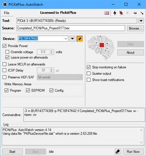
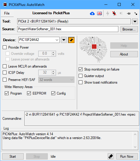
PICKitAutoWatch is a new application and a new approach to programming microcontrollers. PICKitAutoWatch supports both PICkit2 and PICkit3 programmers.  The software is feature rich and easy to use via a simple user interface.

PICKitAutowatch is the best value for money products if you are simply programming your part as it supports the PICkit2 and PICkit3 programmers.

PICKitAutoWatch provides support for the latest generation of Microchip microcontrollers and EEPROMs, and fully supports the  Microchip Programmers-on-Board the Microchip Xpress Boards.

The intent of PICKitAutoWatch is to enable operations with auto-detection and recovery of the program to maintain the programming activity.


PICkitAutoWatch UI

PICKitAutoWatch supports nearly 1000 different types of microcontrollers, EEPROMS and the Microchip Programmers-on-Board the Microchip Xpress Boards..

  • PIC10F, PIC12F, PIC16F, PIC18F, PIC24
  • dsPIC30 and dsPIC33 family
  • A wide range of EEPROMs
  • MCP2502X/5X & HCSxx
  • EEPROM 11LCxx, 24LCxx, 25LCxx and 93LCxx, M25Px and FL127x
  • Microchip Xpress Boards.
  • See here for the full list of supported parts

Core functionality

  • Programs the target part when a new hex file is generated
  • Automatic part detection
  • Recently used parts listed
  • Supports project settings – save and load of project configuration
  • Supports multiple voltages within constraints of physical programmer – noting that some clone programmers do not support voltage control
  • Supports ISCP protocol frequency management
  • Manages Microchip HEF and SAF memory with automatic merger of HEF/SAF memory into target part
  • Support a wide range of Windows operating systems (32bit/64bit): Windows XP ,Windows Vista, Windows 7, Windows Embedded 7, Windows 8, Windows 10
  • New programming protocols to support new classes of Microchips PIC microcontrollers
  • Updated and managed database for Microchip and other EEPROM devices
  • Supports the standard Microchip Microchip PICkit2 and PICkit3 programmer firmware.  PICKitPlus does not require an update to the Microchip PICkit2 and PICkit3 programmer firmware
  • Control power on and off independent of programming state
  • Automatic parts database update
  • Internet connection not required

Internationalization Support

  • Supports local language.

Safe Usage Enhancements

  • Windows toast alerting of programming operations
  • Delays and file retry options
  • Sound notifications
  • Generation of log file with timestamps and automatic deletion

Environments proved to work

  • Windows file structures local hard drive, LAN and WAN shares
  • MPLAB-X IDE
  • MPASMX compiler and linker
  • GPASM compiler and linker
  • MPLAB-X Cloud IDE with remote HEX download to the local file structure
  • There are many, many more

Which parts are supported?

See the PICKitPlus website for the full list of supported parts.

Summary

PICKitAutoWatch is the easiest way to integrate your development tools with the programmer and the microcontroller or EEPROM.

Still to come …..

  • PICKitPlus for Linux
  • PICKitPlus for Pi
  • PICKitPlus Gang Programmer

See the www.pickitplus.co.uk website for more details on PICKitPlus software and hardware products.

Sonar-on-a-chip provides up to 5 metres ToF range

Shipping to strategic customers, the CH-201 MEMS-based ultrasonic Time-of-Flight (ToF) sensor offers an extended sensing range of 5 metres. [via]

This ToF sensor uses a tiny ultrasonic transducer chip that sends a pulse of ultrasound and then listens for echoes returning from targets in the sensor’s field-of-view. TDK’s MEMS ultrasonic technology leverages a proprietary ToF sensor in a 3.5×3.5mm package that combines a MEMS ultrasonic transducer with a power-efficient digital signal processor (DSP) on a custom low-power, mixed-signal CMOS ASIC. The sensor handles a variety of ultrasonic signal-processing functions, enabling customers’ flexible industrial design options for a broad range of use-case scenarios including range-finding, presence/proximity sensing, object detection/avoidance and 3D position-tracking. The devices operates from ultra-low power, supporting always-on sensing in battery powered devices.

TDK – www.tdk.com

NEXCOM NDiS V1000: The 4K Digital Signage Player

Vibrant, 4k resolution multi-displays come to life with NEXCOM’s new NDiS V1000 digital signage player. Powered by AMD’s APU microprocessor, the seamlessly integrated CPU and GPU result in a high performance yet lower-power device perfect for retail environments – and even private use. The value-added and scalable NDiS V1000’s compact design is the result of customer feedback, with just the necessary onboard components (COM, LAN, USB, etc.) and an M.2 expansion slot to meet your everyday needs.

The highest resolution, from the best “APU” for the job

4k resolution is quickly becoming indispensable for quality graphic display and not just a nice option. In building the NDiS V1000 4k signage player, NEXCOM carefully selected the AMD Ryzen™ Embedded V1605 CPU and AMD Radeon™ Vega 8 GPU SoC, supplementing four independent HDMI 2.0 ports, to ensure that quadruple multi-displays will pop with amazing clarity. The integrated SoC also generates less thermal power while achieving better graphic performance than Intel’s, beating their CPU benchmarks with a lower price point. With such outstanding capabilities, it’s no wonder that retail businesses, such as shopping malls, department stores, and convenience stores, keep the NDiS V1000 top of mind. Yet the output quality is so superb and processing so seamless that museums and business war rooms are also in love with the signage player!

We heard you!

We carefully examined customer evaluations of previous digital signage player models in creating the NDiS V1000. First, we heard customers when they said they wanted less noise – hence, the fanless design. Customers also only desired essential components in a smaller size, which you can see in the simple and clean I/O design, with most components relegated to the back of the device. All of these redesigns have the added benefit of reducing power, thus saving you potential costs.

Simple does it

With only the essential components to help you run your business smoothly, the NDiS V1000 is the adaptable and suitable choice for a variety of needs. The onboard COM port is perfect for legacy devices, such as barcode scanners, so that you don’t have to replace equipment to connect to your computers. We also include four USB 3.0 ports for instances where connectivity speed is a priority, making the NDiS V1000 a perfect solution for factory automation and production monitoring and storage. Use the two LAN ports for various tasks, perhaps one for transferring data and displaying information, and the other for private monitoring and security. The M.2 E key expansion slot is customizable to your specific needs but an excellent fit for a Wi-Fi module, which, for example, could help franchisees and stores send data to and receive data from a centralized cloud overnight.

Main Features

  • Onboard AMD V1605B APU processor
  • Graphics processing speed up to 1.1 GHz
  • Dual DDR4 SO-DIMM, up to 32G
  • 4 x HDMI 2.0 for video wall uses
  • 4 x USB 3.0 support
  • Supports M.2 M/B Key, 2280/2242 size storage device
  • M.2 E key slot for optional Wi-Fi module

No pricing or availability information was provided for the NDiS V1000. More information may be found on Nexcom’s announcement and product page.

[via]

Ultra-Low Dropout Linear LED Driver from Diodes Incorporated Extends Lighting Strips

Diodes Incorporated today announced the BCR430UW6 linear LED driver with ultra-low dropout voltage and constant current regulation between 5mA and 100mA. This combination allows more LEDs to be driven from a low supply voltage, making the BCR430UW6 suitable for applications that require multiple LEDs to operate together, such as signage illumination and architectural lighting for commercial and retail installations.

The ultra-low dropout voltage of 115mV and low operating current of just 285μA provides a greater level of system efficiency and scope to drive more LEDs per string reliably. These factors are particularly important in applications where the characteristics of the lighting are essential to the user experience, such as signage and architectural illumination.

The device requires no external power transistors or capacitors, reducing the overall BoM cost and increasing system stability. Long-term reliability is also improved through the robust design, which is tolerant to overvoltage levels resulting from faults in the LEDs or supply transients. Integrated thermal protection limits the output current in the event of high operating temperatures, avoiding operational failure and maximizing the working lifetime of the LEDs.

Features

  • LED Current Tolerance of ±5% at 95mA Output Current
  • Thermal Protection Reduces LED Current at Elevated Temperature
  • Low Typical Saturation Voltage of 115mV at 50mA
  • 5mA to 100mA Adjustable LED Current with an External Resistor
  • 5V to 42V Supply Voltage
  • High Power 1W Dissipation in SOT26
  • No External Capacitors Required for Stable Operation
  • LED Dimming Using PWM
  • Parallel Devices to Increase Regulated Current

With an adjustable output current level between 5mA and 100mA, the BCR430UW6 can provide greater flexibility, allowing a single design to be used to drive various LED configurations. The output is highly stable, held at ±5% across temperature variations and supply voltage fluctuations. This stability delivers a uniform output lighting level under all operating conditions.

Other advanced features include PWM-based dimming, an operating voltage range of 5V to 42V, and support for parallel operation to further increase the regulated output current.

The BCR430UW6 is provided in a SOT26 package. Further information is available at www.diodes.com

650 V half-bridge SOI driver families with integrated bootstrap diodes offers superior robustness

Infineon Technologies AG broadens its EiceDRIVER™ portfolio with the 650 V half-bridge gate drivers based on Infineon’s unique silicon on insulator (SOI) technology. The products provide leading negative transient voltage immunity, monolithic integration of a real bootstrap diode, and superior latch-up immunity for MOSFET and IGBT based inverter applications. These unique features enable more robust and reliable designs at reduced BOM cost. The high output current family 2ED218x is tailored for high frequency applications like induction cooking, air conditioning compressors, SMPS, and UPS. The low output current family 2ED210x is targeting home appliances, power tools, motor control and drives, fans and pumps.

2ED218x is the 2.5 A high current EiceDRIVER family, while 2ED210x is the 0.7 A low current family. They include variants with shutdown functionality and separate logic and power ground. The integrated bootstrap diode offers ultra-fast reverse recovery with a typical 30 Ω on-resistance. A negative VS immunity of -100 V with repetitive 300 ns wide pulses provides superior robustness and reliable operation. Additionally, integrated dead-time with cross-conduction logic and independent under-voltage lockout (UVLO) for high and low side voltage supplies support safe operation. The propagation delay of the gate driver family amounts to 200 ns.

Features

  • Operating voltages (VS node) up to +650V
  • Negative VS transient immunity of 100V
  • Integrated ultra-fast, low resistance bootstrap diode, lower the BOM cost
  • High and low voltage pins separated for maximum creepage and clearance
  • Separate logic and power ground
  • Floating channel designed for bootstrap operation
  • Maximum supply voltage of 25V
  • Independent under voltage lockout (UVLO) for both channels
  • 200ns propagation delay
  • HIN, LIN input logic
  • Logic Operational up to –11V on VS Pin
  • Negative Voltage Tolerance On Inputs of –5V
  • The floating channel can be used to drive an N-channel MOSFET, SiC MOSFET or IGBT in the high side configuration

Typical Application

Availability

2ED218x and 2ED210x are pin-to-pin, electrically and functionally, compatible with earlier generation IR(S)218x and IR(S)210x devices. They are available in industry standard DSO-8 (SOIC8) and DSO-14 (SOIC-14) packages with 2 kV HBM ESD rating (2ED218x only). Both the 2ED218x and 2ED210x product families can be ordered as production samples and in high volume. More information is available at www.infineon.com/SOI

3D Image Sensor REAL3 for Face Authentication announced at CES 2020

Infineon Technologies AG has collaborated with software and 3D Time-of-Flight (ToF) system specialist pmdtechnologies ag to develop reportedly the world’s smallest, most powerful 3D image sensor. Designated the REAL3, the single-chip solution measures just 4.4 x 5.1 mm and is the fifth generation of time-of-flight deep sensors from Infineon. The sensor can be incorporated into even the smallest devices with just a few elements while providing high resolution with low power consumption.

The depth sensor ToF technology enables an accurate 3D image of faces, hand details or objects which is relevant when it must be ensured that the image matches the original. This is already applied in payment transactions using mobile phones or devices that need no bank details, bank cards or cashiers and the payment is carried out instead via facial recognition. This in turn requires reliable and secure image and return transmission of the high-resolution 3D image data.

“With the fifth generation of our REAL3 chip we are once again demonstrating our leading position in the field of 3D sensors,” said Andreas Urschitz, President of the Power Management and Multimarket Division at Infineon, in a statement. “It’s robust, reliable, powerful, energy efficient and at the same time decisively small.”

The 3D sensor also allows the device to be controlled via gestures, so that human-machine interaction is context-based and without touch.

The sensor chip (IRS2877C) provides additional options for ambitious photos with cameras, for example, with enhanced autofocus, bokeh effect for photo and video, and improved resolution in poor lighting conditions. Real-time full-3D mapping also allows authentic augmented reality experiences to be presented.

The chip was developed in Graz, Dresden and Siegen and combines the expertise of Infineon’s and pmdtechnologies’ German and Austrian locations. Production will begin in mid 2020. In addition, Infineon Technologies offers an optimized illumination driver (IRS9100C) that further improves performance, size and cost as a complete solution.

The sensor is the basis of pmdtechnologies latest 3D Time-of-Flight camera module. The module provides a VGA resolution depth data output and incorporates a newly designed 5µm pmd pixel core. The imager’s VGA resolution enables applications to produce more detailed 3D data. Uses include enhanced photography, 3D reconstruction of faces and objects, augmented reality, photorealistic relighting, and gesture control and measurement.

[via]

Meet the Arduino Portenta!

CES 2020 has been full of the usual intrigue and amazing display of technological advancements across different industries. As usual, it has featured the release/launch of several new products by different companies and one of such announcements we know will interest the community, is the launch of the Arduino Portenta Family of Boards, with the first member of the family; The Portenta H7 board.

The Portenta H7

The Portenta Family was created to fill the need for industry-grade boards and the first member of the family; the Portenta H7, shows they mean business as it was announced alongside a companion board; called the Portenta Carrier Board, which will leave you with an impression of this being baby steps towards Arduino getting into the SBCs and Embedded Gateways space.

The Portenta H7 is built around the STMicro STM32H747XI which implements a dual-core comprising of Arm Cortex-M7 (running at 480MHz ) and a Cortex-M4(running at 240MHz) on-chip. The dual-core nature enables applications that allow users to simultaneously run high-level code along with real-time tasks. It was consciously designed for industrial applications, with specific features that make it suitable for such an environment, like support for operating temperatures between -40° and 85°C.

Back View showing 2×80 IO Pins

Some of the features and specifications of the Portenta H7 include:

  •  STM32H747XI Microcontroller with ARM Cortex-M7  and Cortex-M4
  • 2MB SDRAM
  • 16MB QSPI NOR Flash
  • MXP SE0502 onboard Security
  • Bluetooth 5.1
  • 2.4GHz WiFi 802.11b/g/n
  • On-board 10/100M PHY
  • MIPI DSI with an 8-bit camera interface via an 80-pin connector
  • Single USB 2.0 Type-C port for power, programming, and DisplayPort (MIPI DSI)
  • Arduino MKR headers with UART1, 6x Analog input pins, GPIO, PWM, SPI, I2C, Reset, 5V, 3.3V, and GND
  • 2x 80 pin high-density connectors which can be accessed via the Portenta Carrier Board to provide access to additional ports like; UART (4), CAN Bus(1), USB2.0(2), I2C(2), SPI(2), ADC(8 16-bits), DAC(2 12-bits), GPIO(6), I2S, DMIC, and SAI.
  • 22 timers and watchdogs
  • Supports up to 5V via USB-C port or VIN pin
  • Supports Power to board via a 3.7V Single-Cell LiPo Battery with an Integrated Charger
  • Temperature Range – -40 °C to +85 °C (excl. Wireless module) / -10 °C to +55 °C (incl. Wireless module)

Some of the specs provided above can be customized to suit the user’s needs. For instance, memory could be increased to 64 MByte of SDRAM, and 128 MByte of QSPI Flash, an external UFL antenna connector could be added to the board, and you can choose between crypto-chips from Microchip® or NXP.

Showing an understanding of how much things has changed around embedded systems development, the Portenta H7, asides support for Codes written with the Arduino IDE, supports MicroPython and JavaScript code out of the box, making the board more useful to a broader category of developers including those not so familiar with C. Still on Programming, the Portenta H7 also supports the Arm Mbed OS IoT operating system, whose enterprise-grade features will be useful in any industrial application for which the board is deployed.

The Portenta Carrier Board

The Portenta H7 is currently being promoted alongside the Arduino Pro IDE and the ARM Pelion IoT platform, as an all-in-One suite for IoT Solutions. It is already available for Pre-Order at $99.99 with delivery by the end of February. More information on the board can be found on Arduino’s Website.

The Portenta Carrier Board appears to still be in development and as such, most of the details may still change, but based on pictures and information available online, it helps transform the Portenta into an eNUC computer and exposes all of the H7 physical interfaces. More information on the Carrier board can be found here.

SAMD21G18A Development Board

An Open Source SAMD21 Development Board by sirmylesavery @ hackaday.io

This project started after my first introduction to PCB design at my 2019 summer internship. At that internship, I designed a board that used a SAMD21 to control a GPS and LoRa module. This was my first introduction to the SAMD21 MCU and I immediately was interested in its capabilities. As a side project to work, I started to design a development board centered around this module.

SAMD21G18A Development Board – [Link]

18V, 2A, Single-Phase, BLDC Motor Driver with Integrated Hall Sensor

The MP6650 is a single-phase, brushless, DC motor driver with integrated power MOSFETs and a Hall-effect sensor. The device drives single-phase brushless DC fan motors with up to 2A of output current. The IC has a 3.3V to 18V input voltage range and input line reverse-voltage protection (RVP) to save the external diode on the supply line.

The device controls the rotational speed through the PWM signal on the PWM pin. It has a rotational speed detection feature and rotor lock fault indication on the FG/RD pin with an open-drain output. The output speed vs. the input duty curve can be configured easily for flexible use. To reduce audible fan driver noise and power loss, the MP6650 features a soft on/off phase transition and an automatic phase-lock function of the motor winding BEMF and current.

Full protection features include input over-voltage protection (OVP), under-voltage lockout (UVLO), rotor deadlock (RD) protection, thermal shutdown, and input reverse protection.

The MP6650 requires a minimal number of external components to save solution cost. It is available in TSOT23-6-L, TSOT23-6-R, TSOT23-6-SL, and TSOT23-6-RSL packages.

Summary of Features & Benefits

  • Embedded Hall Sensor with High Sensitivity
  • Wide 3.3V to 18V Operating Input Range
  • Up to 2A Configurable Current Limit
  • Integrated Power MOSFETs: Total 740mΩ (HS-FET and LS-FET)
  • Configurable Speed Curve
  • Built-In Adjustable Speed Curve Corner Setting
  • Automatic Phase-Lock Detection of Winding BEMF and Current Zero-Crossing
  • Soft On/Off Phase Transition
  • Rotational Speed Indicator (FG) Signal
  • 2kHz to 100kHz PWM Input Frequency Range
  • Fixed 26kHz Output Switching Frequency
  • Input Line Reverse Voltage Protection (RVP)
  • Rotor Deadlock (RD) Protection
  • Thermal Protection and Automatic Recovery
  • Built-In Input OVP, UVLO, and Automatic Recovery
  • Available in TSOT23-6-L, TSOT23-6-R, TSOT23-6-SL, and TSOT23-6-RSL Packages

more information: Monolithic Power Systems Inc.

Meet the ArticKoala! The FPGA Development Board Based on Lattice CrossLink-NX

Barely a week after Lattice semiconductor announced the launch of the CrossLink-NX family of FPGA, Greg Davill, in his amazing way of posting the entire development process in a twitter thread, has announced the launch of a development board based on the Lattice Crosslink-NX 72QFN.

The new board which is called the ArcticKoala was created using some of the sources from recent FPGA tools like the iCEBreaker ICE40-UP5K board. The board comprises of a Lattice Semiconductor LIFCL-40 CrossLink FPGA with a Winbond 25Q128 128Mbit Flash memory (for configuration bitstreams). In terms of interfaces, the board comes with 3x Pmod extension headers, 1x MIPI extension header, and a FTDI FT2232 USB-Serial converter to allow users to connect to the board over USB.

The CrossLink-NX family, on which the new development board is based, was designed using the new Lattice Nexus platform, which combines a 28 nm FD-SOI manufacturing process with a new, Lattice-designed, FPGA fabric architecture optimized for low power operation in a small form factor.

According to Gordon Hands, Director of Product Marketing at Lattice Semiconductor, asides from being super low power (up to 75% compared with similar class devices) and coming with better performance than most FPGAs in its class, the CrossLink-NX is supported by a robust library of design software, IP blocks and application reference designs which makes it quick and easy for developers to integrate it into new or existing designs.

Some of the features CrossLink-NX which the ArcticKoala will be breaking out to users include:

  • A Low power FPGA Development Board
  • Highly reliable FPGA with SER up to 100 times lower than other FPGAs in its class.
  • 2.5 Gbps Hardened MIPI D-PHY
  • 5 Gbps PCIe
  • 1.5 Gbps programmable IO
  • 1066 Mbps DDR3.
  • Support for LVDS, subLVDS, OpenLDI (OLDI), SGMII, and FPGA fabric for signal aggregation, duplication, and splitting.
  • High Memory to Logic Ratio (170bits of memory for every logic cell)
  • Instant-on Performance thanks to Ultra-Fast IO configuration (3ms) and total device configuration of 15ms.

Asides from the satirical nature of the name, to create a full-blown board based on an FPGA chip that was released 1 week earlier, confirms the brilliance, impressive talent, and work ethics that the ecosystem has come to respect Davil for.

The board, as usual with Davill, is open source and you can find all the source files on the project’s Github page. More information on the project is available on his tweet about the board.

TOP PCB Companies