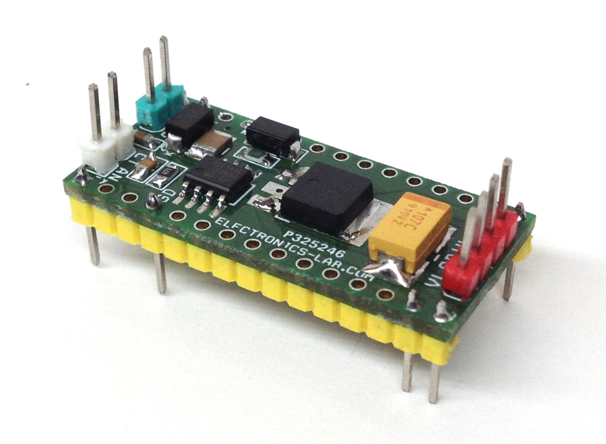
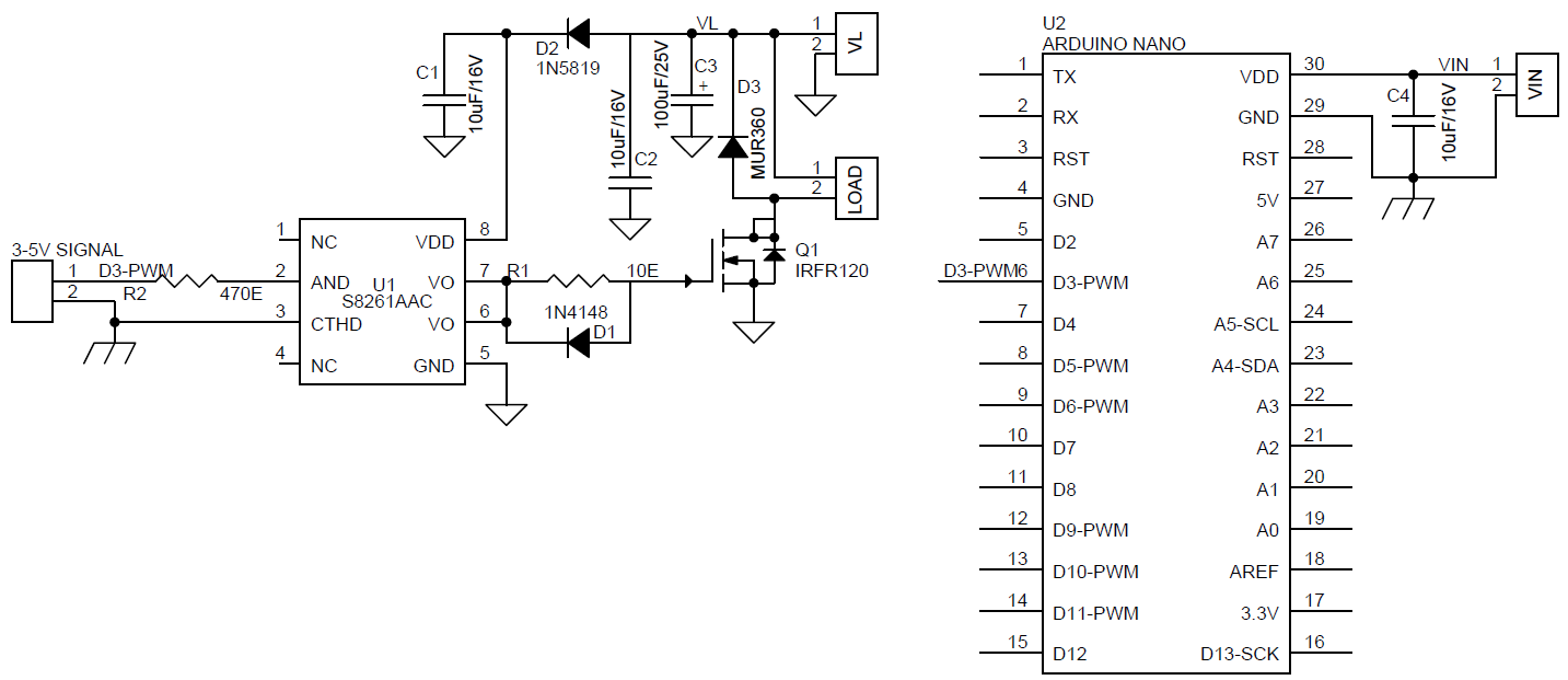
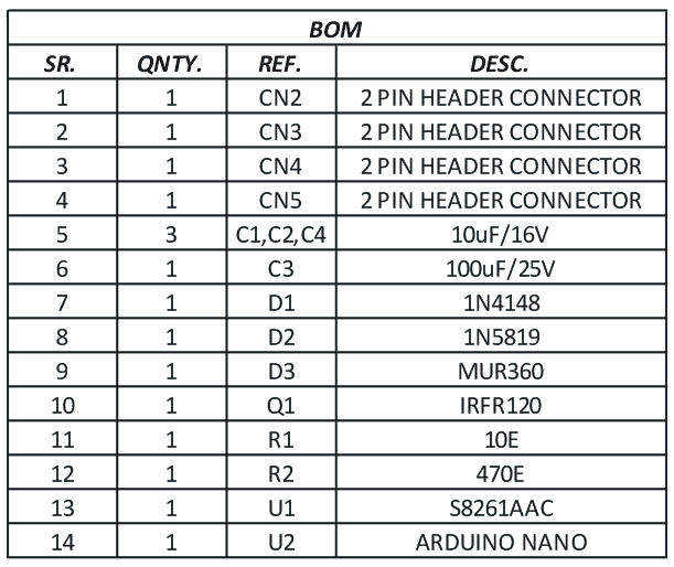
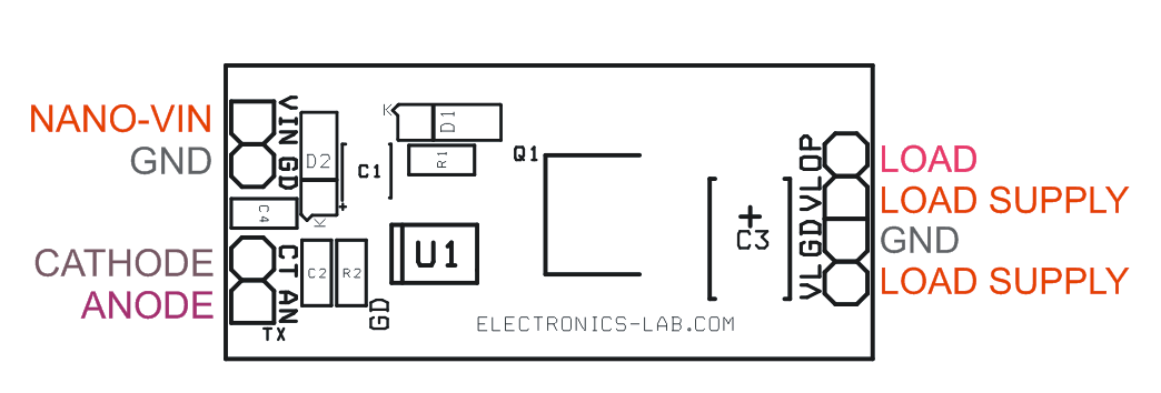
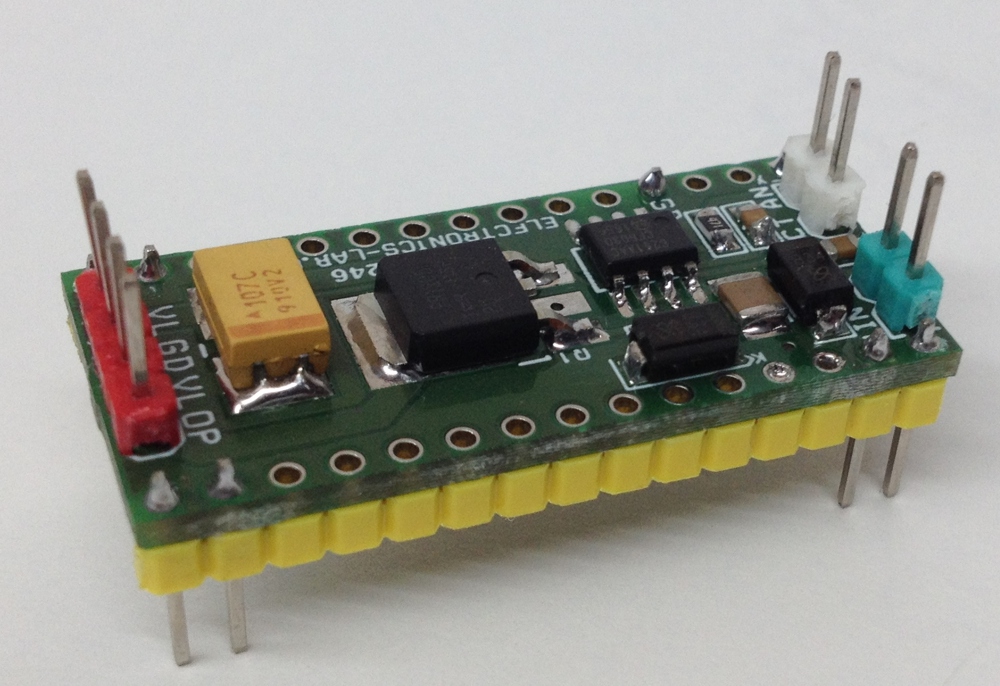
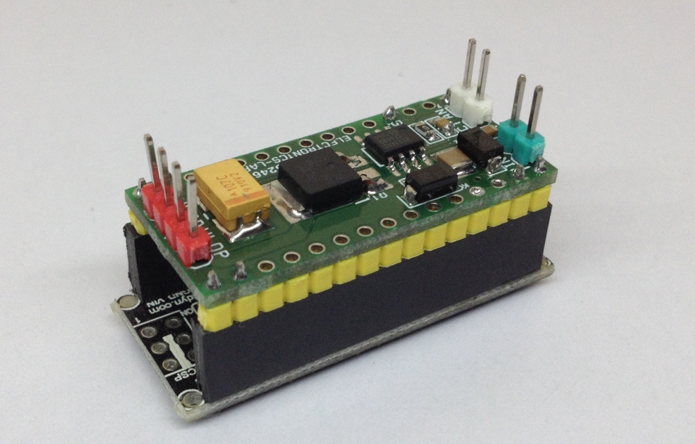
This is an Isolated gate driver-based N channel Mosfet Arduino Nano shield based on Si8261ACC, which can be used in various applications like DC Motor driver, solenoid driver, led driver, bulb driver and heater driver, with 3A fast switching diode provided across the output for an inductive load which protects the circuit from back EMF. Arduino Nano can be used to generate on/off signal or PWM for speed control. The board can also be used as a standalone driver by feeding 3-5V directly to the LED of the Si8261ACC gate driver. MOSFET can handle up to load 3A and DC supply at 12-24V DC. PWM Pin D3 of Arduino connected to gate driver IC.
Isolated Gate MOSFET Driver Based DC Motor and Solenoid Driver Arduino Nano Shiled – [Link]
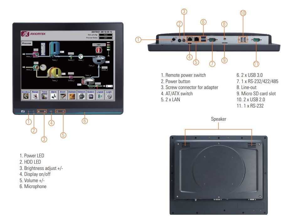
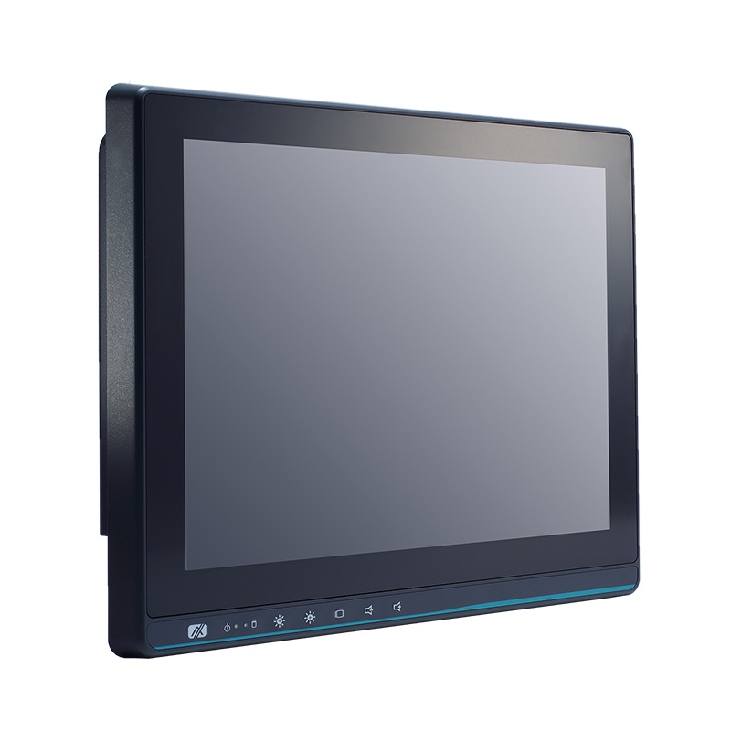
Axiomtek – a world-renowned leader relentlessly devoted in the research, development and manufacture of series of innovative and reliable industrial computer products of high efficiency – is pleased to introduce the GOT115-319, a 15-inch fanless touch panel computer with a thickness of only 50 mm for used in space-constrained environments. It is powered by the Intel® Celeron® processor N3350 or Intel® Pentium® processor N4200 with the Intel® GFX controller onboard. The GOT115-319 has a 15-inch XGA TFT LCD display with a projected capacitive multi-touch or resistive touch optional touchscreen, 300 nits of brightness and LED backlight. It is a cost-effective solution to achieve a high degree of stability and adaptability for use in multimedia kiosks or as a human machine interface (HMI) for smart manufacturing and rugged retail fields.
“Axiomtek’s 15” XGA GOT115-319 has 1024 x 768 resolutions. It has five programmable OSD function keys on the front panel for users to easily adjust LCD on/off, brightness and volume. Moreover, this compact touch panel computer offers easy access to storage and RAM,” said Frank Chang, a product manager of Product PM Division at Axiomtek. “The robust industrial touch panel PC GOT115-319 has an ultra-slim housing for use in space-constrained environments. It can operate reliably in harsh environments with its wide operating temperature of 0°C to +50°C and vibration endurance for up to 2G.”
The GOT115-319 features rich I/O connectivity. It is equipped with two GbE LAN ports, two USB 2.0 ports, two USB 3.0 ports, one RS-232 port and one RS-232/422/485 port with RI/5V/12V which is selectable by BIOS and one Line-out. Other features include one power button, one remote power switch and one screw-type connector for power. In addition, there is an easily accessible external switch for AT/ATX mode selection and built-in speakers and microphone for multimedia applications. The GOT115-319 supports one full-size PCI Express Mini Card slot and one M.2 Key E slot for RFID and wireless network module installation. The ultra-slim panel computer is equipped with one 204-pin DDR3L-1600 SO-DIMM with up to 8GB of memory capacity. It also offers one 2.5″ SATA HDD/SSD, one mSATA and one MicroSD card for storage. To meet diverse installation requirements, it supports panel mount, wall mount, VESA arm and desktop stand.
Advanced Features:
15″ XGA TFT LCD display with LED backlight
Fanless design with Intel® Celeron® processor N3350 or Intel® Pentium® processor N4200
2 GbE LAN, 4 USB and 2 COM (1 x RS-232/422/485)
IP65-rated plastic front bezel
Supports RFID and wireless module (optional)
External AT/ATX mode selection switch
Easy access storage & RAM design
Supports panel mount, wall mount, VESA arm and desktop stand
RS-232/422/485 with RI/5V/12V selectable by BIOS
Programmable OSD function key
Axiomtek’s GOT115-319 is now available for purchase. For more product information or customization services, please visit our global website at www.axiomtek.com or contact one of our sales representatives at info@axiomtek.com.tw.
This is an Isolated gate driver-based N channel Mosfet Arduino Nano shield based on Si8261ACC, which can be used in various applications like DC Motor driver, solenoid driver, led driver, bulb driver and heater driver, with 3A fast switching diode provided across the output for an inductive load which protects the circuit from back EMF. Arduino Nano can be used to generate on/off signal or PWM for speed control. The board can also be used as a standalone driver by feeding 3-5V directly to the LED of the Si8261ACC gate driver. MOSFET can handle up to load 3A and DC supply at 12-24V DC. PWM Pin D3 of Arduino connected to gate driver IC.
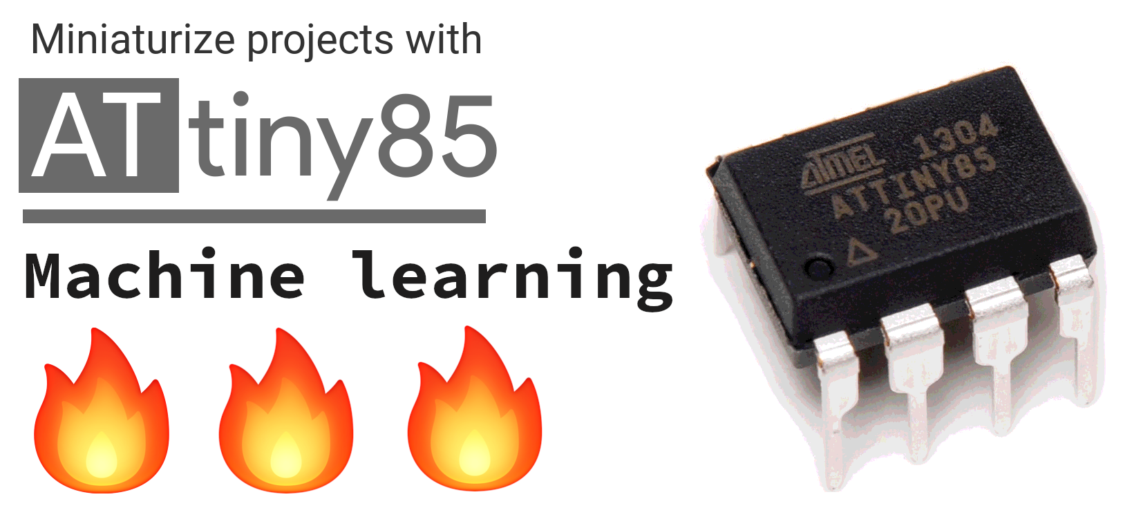
When I first run a Machine learning project on my Arduino Nano (old generation), it already felt a big achievement. I mean, that board has only 32 Kb of program space and 2 Kb of RAM and you can buy a chinese clone for around 2.50 $.
It already opened the path to a embedded machine learning at a new scale, given the huge amount of microcontrollers ready to become “intelligent”.
But it was not enough for me: after all, the MicroML generator exports plain C that should run on any embedded system, not only on Arduino boards.
So I setup to test if I could go even smaller and run it on the #1 of tiny chips: the Attiny85.
AAEON’s UP project has launched an edge computing enabled kit called the UPX Edge. The system which was developed to power industrial automation, robotics, AI, and IoT applications, is built around the Intel 8th Gen Whiskey Lake-U based UP Xtreme board and comes preloaded with an Ubuntu 18.04 image based on Linux kernel 5.0
It was initially available on Kickstarter as the “UP Xtreme Pro” or “UP Xtreme AI Pro” (if u selected the option of a UP AI Core XM2280 M.2 module) with a price tag of $150 is now available at $499 with various processor options, including the UP AI Core module which will set you back a further $139 on the Core i7-8665UE and i5-8365UE SKUs. Asides the price difference, compared to the prototype advertised on Kickstarter, the new UPX Edge system also comes with all the UP Xtreme’s real-world coastline ports exposed and offers a wider -20 to 70°C operating temperature range compared to the originally listed -20 to 60°C, which is maintained even when the AI Core Module is added to it.
Unlike the UPX SBC, the UPX Edge chassis version brings forth the UP Xtreme’s RS232/422/485 headers as 2x DB9 COM ports, and there’s also a jack-style RS232 serial port and a USB port which the SBC product page listed as a USB 3.0 ports but the UPX Edge refers to them as a USB 3.2 Gen 1 port. This must, however, be a typo since there is no specific reference to the USB ports being upgraded.
Asides the various ports mentioned above, the UPX Edge also extends the 40-pin and STM32-related GPIO as Phoenix connectors on either side of the system with an audio jack, a 4x antenna connectors, and optional VESA and DIN-rail mounting also provided.
The system has a consumption average of 26W and is designed to be powered by a 12-60V DC power supply with a lockable connector and power button.
The UP Xtreme Edge Compute Enabling Kit (UPX Edge) is available for pre-order on it’s UP shopping page starting at $499, with shipments due in January. The re-launched UP Xtreme SBC, on the other hand, is available starting at $299. More information on both products can be found on Aeon’s announcement for the launch of both products.
Lattice Semiconductor has introduced a new low power FPGA platform that has been designed for a wide range of applications. by Ally Winning @ eenewseurope.com
The Lattice Nexus platform provides system-level solutions that combine design software and pre-engineered soft IP blocks with evaluation boards, kits and reference designs. The platform has new architectural features that optimise system performance at low power. Its optimised DSP blocks and higher on-chip memory capacity allow applications such as AI inferencing algorithms, to run twice as fast at half the power of previous Lattice FPGAs.
The Lattice Nexus platform is based on Samsung’s high-volume 28 nm fully-depleted silicon-on-insulator (FD-SOI) process technology, which has 50% lower transistor leakage compared to bulk CMOS.
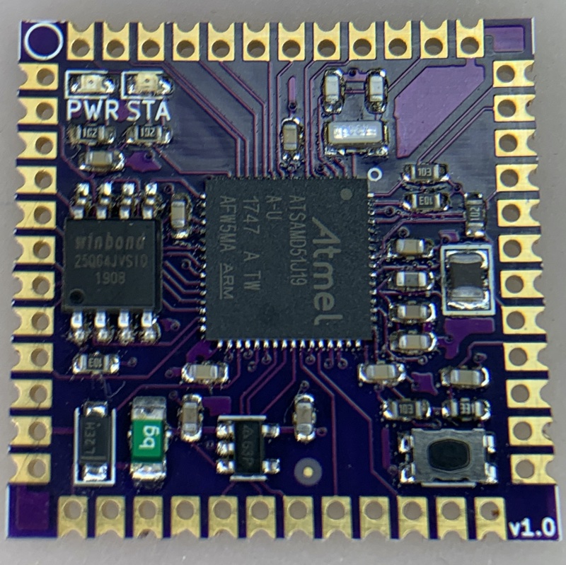
As you would expect from a stack backed by giants like Adafruit, CircuitPython is overthrowing Micropython and fast becoming one of the most popular stacks for embedded development amongst makers. As a result of this popularity, quite a number of CircuitPython optimized boards are springing up and one of the latest ones is CircuitBrains which is a brainchild (notice the pun?) of Kevin Neubauer.
According to Kevin, the new board which run an ATSAMD51J19A Microcontroller (32-bit ARM Cortex M4) at 120 MHZ, with 192kB of SRAM and 512KB of Flash, was born out of his desire to modularize the core of CircuitPython boards (MCU, clock, power, decoupling, and flash) and package it in a way similar to the ESP-12 modules so they could “just be soldered on” to a daughterboard that contains peripheral components needed to make the board fully functional.
With this, Kevin was hoping to overcome the limited choices makers have around small form-factors for Circuit Python-based boards. According to kelvin; “when it comes to finishing up a CircuitPython project, I felt limited in choice for a small form-factor, streamlined board. I always ended up creating my own boards. The overhead in doing this was huge though. You have to make sure your design has proper power, decoupling, and clock. Then you source all of the parts. After that you layout the PCB and have it fabricated. When the PCB and parts arrive, you have to deal with finicky small-pitch surface mount assembly. Finally, you need to download the sources for the UF2 bootloader and CircuitPython and define your board, compile, and flash. This makes what should be a small project pretty time consuming and tedious!”.
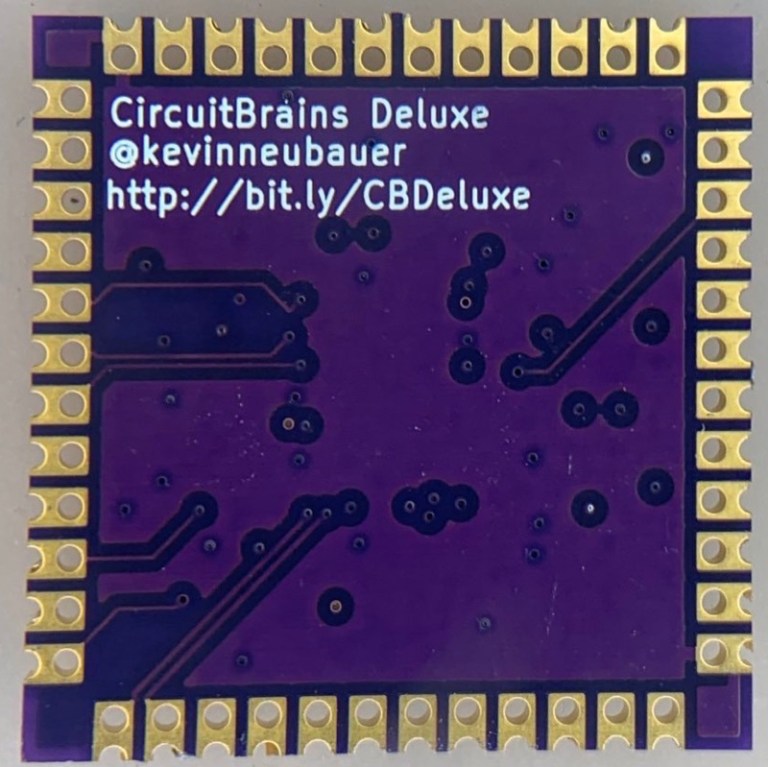
CircuitBrain Deluxe Back View
His idea was a board with a reusable design that could be pulled off the shelf and dropped into a project, without significantly changing the size of the project.
Some of the specifications kelvin penned down for the boards are provided below;
Dimensions: 29 x 29 x 3.5 millimeters / 1.15 x 1.15 x 0.15 inches
Atmel ATSAMD51J19A Microcontroller (32-bit ARM Cortex M4)
120 MHz
192 KB SRAM
512 KB Flash
8 MB SPI Flash
Onboard 3.3V LDO Regulator
Power and Status LEDs
Breakouts for SPI and I2C
Breakouts for 14 Analog and 19 Digital Inputs/Outputs
While the boards are currently in the prototyping/testing stage, Kelvin has already provided the schematics and PCB files for the board on the project’s Github Repo.
Work is still ongoing and you can get more info about the project, or follow its progress via the project’s page on Kelvin’s Blog.
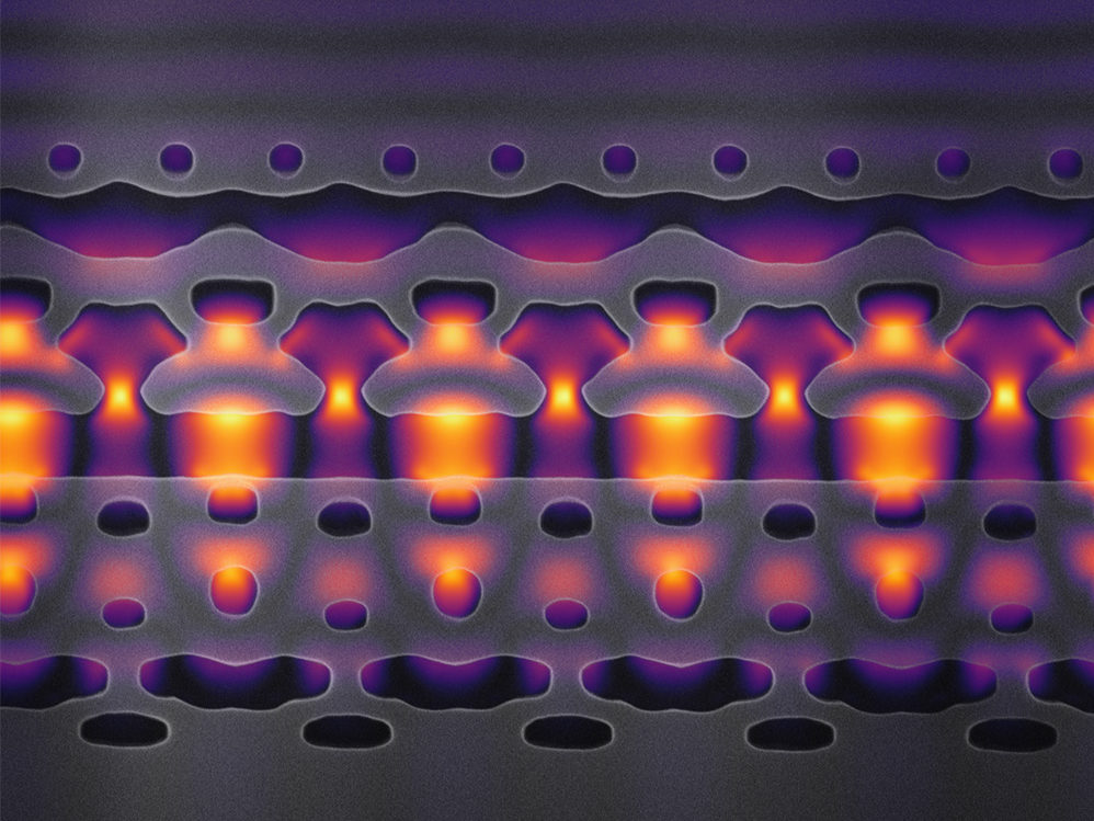
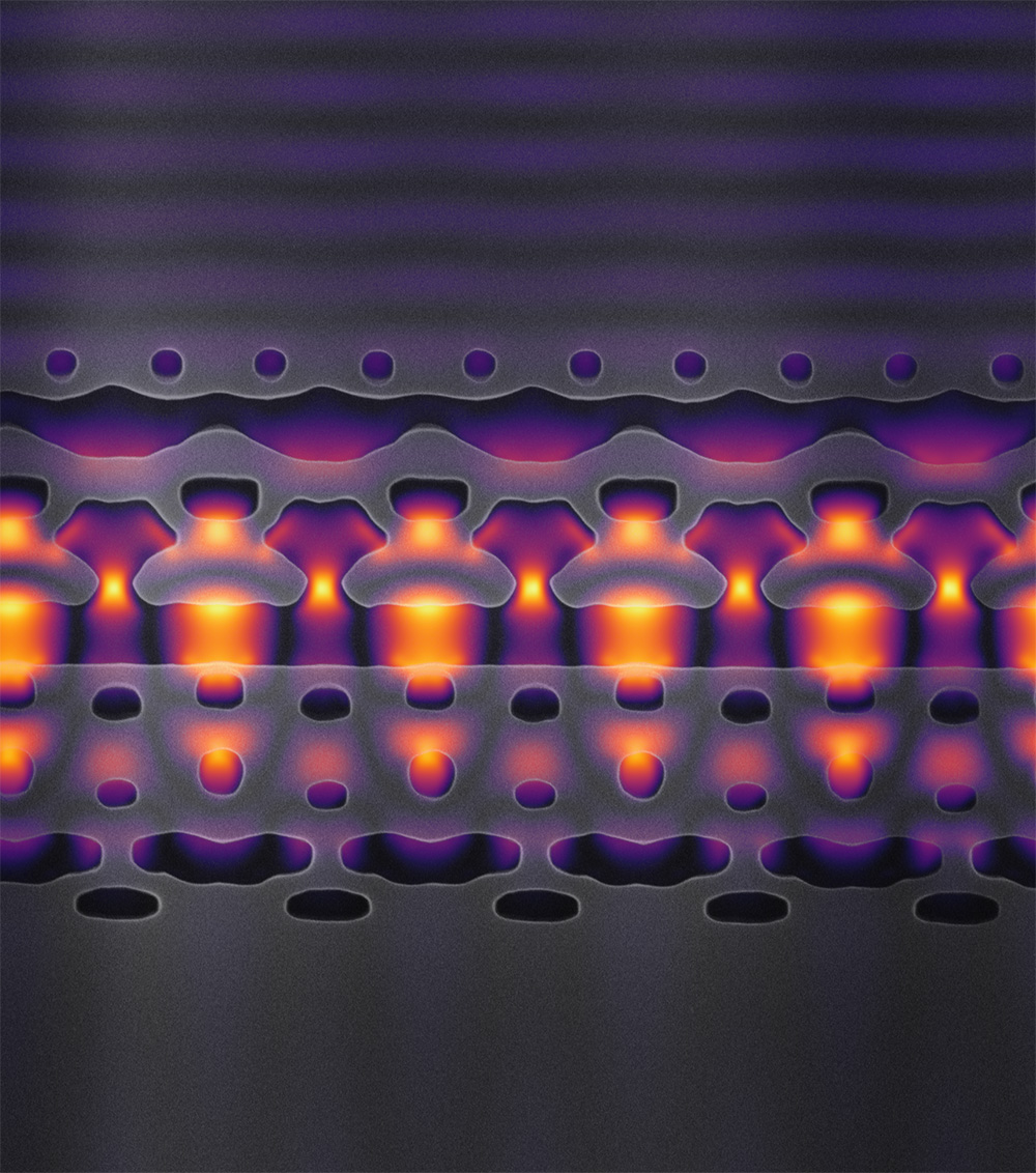
Researchers at Stanford University have demonstrated the acceleration of electrons through what they describe as an “On-chip integrated laser-driven particle accelerator”, detailed in a recent paper published in the Science journal. by Tom Abate
On a hillside above Stanford University, the SLAC National Accelerator Laboratory operates a scientific instrument nearly 2 miles long. In this giant accelerator, a stream of electrons flows through a vacuum pipe, as bursts of microwave radiation nudge the particles ever-faster forward until their velocity approaches the speed of light, creating a powerful beam that scientists from around the world use to probe the atomic and molecular structures of inorganic and biological materials.
This image, magnified 25,000 times, shows a section of an accelerator-on-a-chip. The gray structures focus infrared laser light (shown in yellow and purple) on electrons flowing through the center channel. By packing 1,000 channels onto an inch-sized chip, Stanford researchers hope to accelerate electrons to 94 percent of the speed of light. (Image credit: Courtesy Neil Sapra)
Now, for the first time, scientists at Stanford and SLAC have created a silicon chip that can accelerate electrons – albeit at a fraction of the velocity of that massive instrument – using an infrared laser to deliver, in less than a hair’s width, the sort of energy boost that takes microwaves many feet.
Writing in the Jan. 3 issue of Science, a team led by electrical engineer Jelena Vuckovic explained how they carved a nanoscale channel out of silicon, sealed it in a vacuum and sent electrons through this cavity while pulses of infrared light – to which silicon is as transparent as glass is to visible light – were transmitted by the channel walls to speed the electrons along.
The accelerator-on-a-chip demonstrated in Science is just a prototype, but Vuckovic said its design and fabrication techniques can be scaled up to deliver particle beams accelerated enough to perform cutting-edge experiments in chemistry, materials science and biological discovery that don’t require the power of a massive accelerator.
“The largest accelerators are like powerful telescopes. There are only a few in the world and scientists must come to places like SLAC to use them,” Vuckovic said. “We want to miniaturize accelerator technology in a way that makes it a more accessible research tool.”
Team members liken their approach to the way that computing evolved from the mainframe to the smaller but still useful PC. Accelerator-on-a-chip technology could also lead to new cancer radiation therapies, said physicist Robert Byer, a co-author of the Science paper. Again, it’s a matter of size. Today, medical X-ray machines fill a room and deliver a beam of radiation that’s tough to focus on tumors, requiring patients to wear lead shields to minimize collateral damage.
“In this paper we begin to show how it might be possible to deliver electron beam radiation directly to a tumor, leaving healthy tissue unaffected,” said Byer, who leads the Accelerator on a Chip International Program, or ACHIP, a broader effort of which this current research is a part.
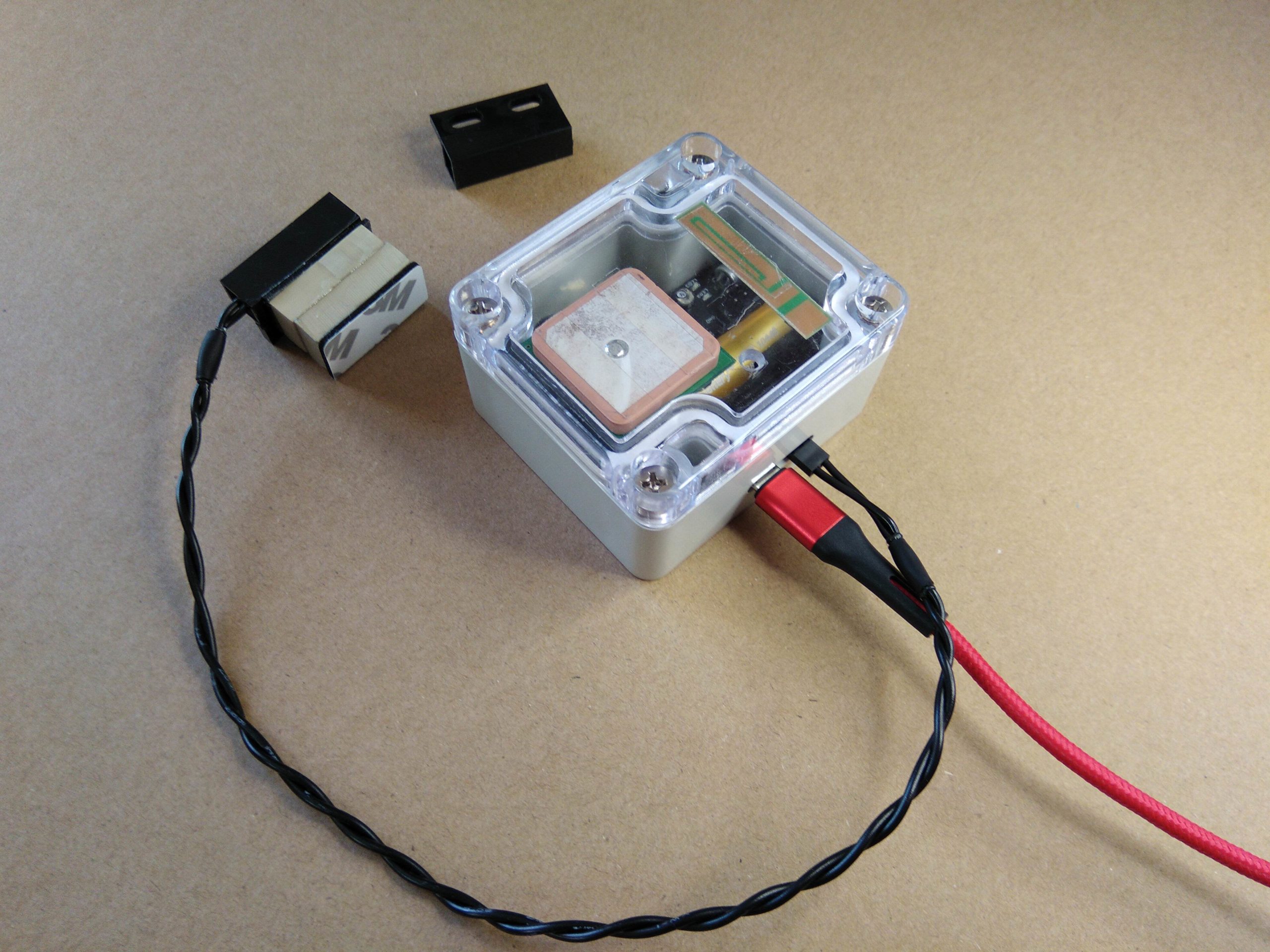
Zak Kemble published another great project. This time it’s a Remote Mail Notifier with GPS functionality. He writes:
At the moment I’m living in a block of flats and my mailbox is in a central lobby area. I’m often receiving small surprise packets from China and never know when the postman has been, usually between 8 and 12, sometimes even twice a day! I also don’t have any road facing windows that I can look out of for the bright red Royal Mail van.
So, I wanted to make something that can notify me of when the postman comes by and pops something into my mailbox. The previous place I lived at had the mailboxes at the far end of a gated car park, not great when it’s cold and wet!
I can’t have any cables going from the mailbox to my flat of course, so a wireless solution is needed. The first choice would have been to use WiFi, but the mailboxes are too far to get a signal to my back to my flat. I could probably use some kind of 433MHz radio module with a receiver in my flat, but I had recently come across A9G GPRS/GPS modules from A.I. Thinker that can have custom firmware loaded onto them. They only cost around £4 each, and it would also mean I don’t have to deal with annoying AT command parsing like with the popular SIM800. In the end I decided to go with the A9G and add secondary functions of being a listening bug and GPS tracker since it also has a built-in GPS receiver!
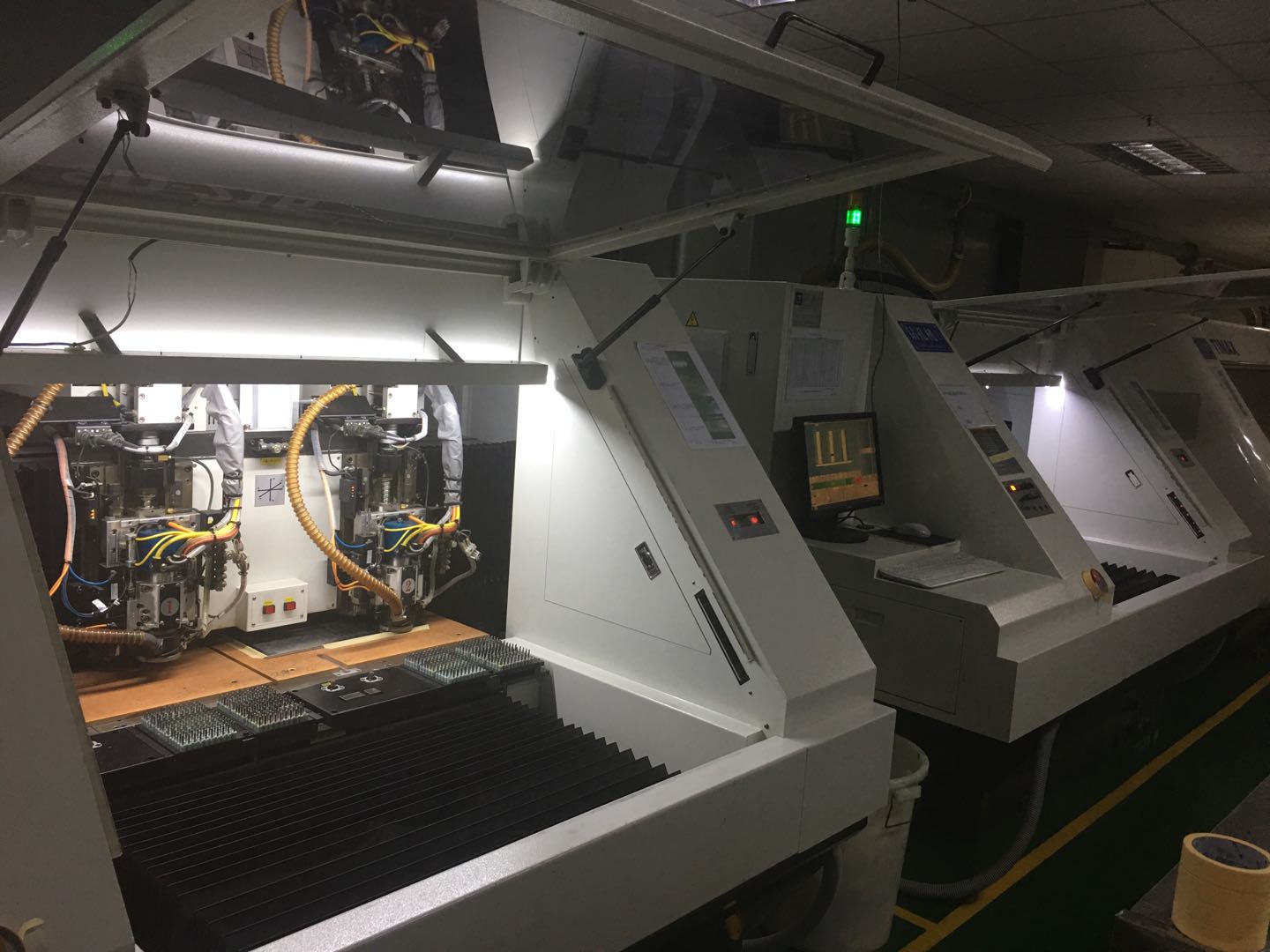
Printed Circuit boards are an important part of the development of any electronic product. They provide easy, neat, and repeatable ways of connecting components together. Thus, ensuring quality from their design to production is so critical that, failure at any point in the process could lead to a lot of money going to waste and delay in the project timeline, as such, the existence of several EDA software ensures the reliable design, the focus should then be on ensuring a manufacturer that is worth his weight in Gold, is selected for the manufacturing of the designs. One such manufacturer with experience and interesting capabilities is NextPCB and for today’s review, we will examine their processes, rates, and why you should probably choose (or not choose) them as PCB manufacturers for your next PCB project.
NextPCB is reputed as one of the most popular PCB manufacturers in China. Situated at the heart of Shenzhen, NextPCB has been in the PCB manufacturing and assembly industry for over 15 years, providing some of the most innovative printed circuit boards, with assembly technologies of the highest quality standards, the fastest delivery turnaround (as fast as 24 hours), lowest manufacturer direct prices, and support via dedicated customer service professionals.
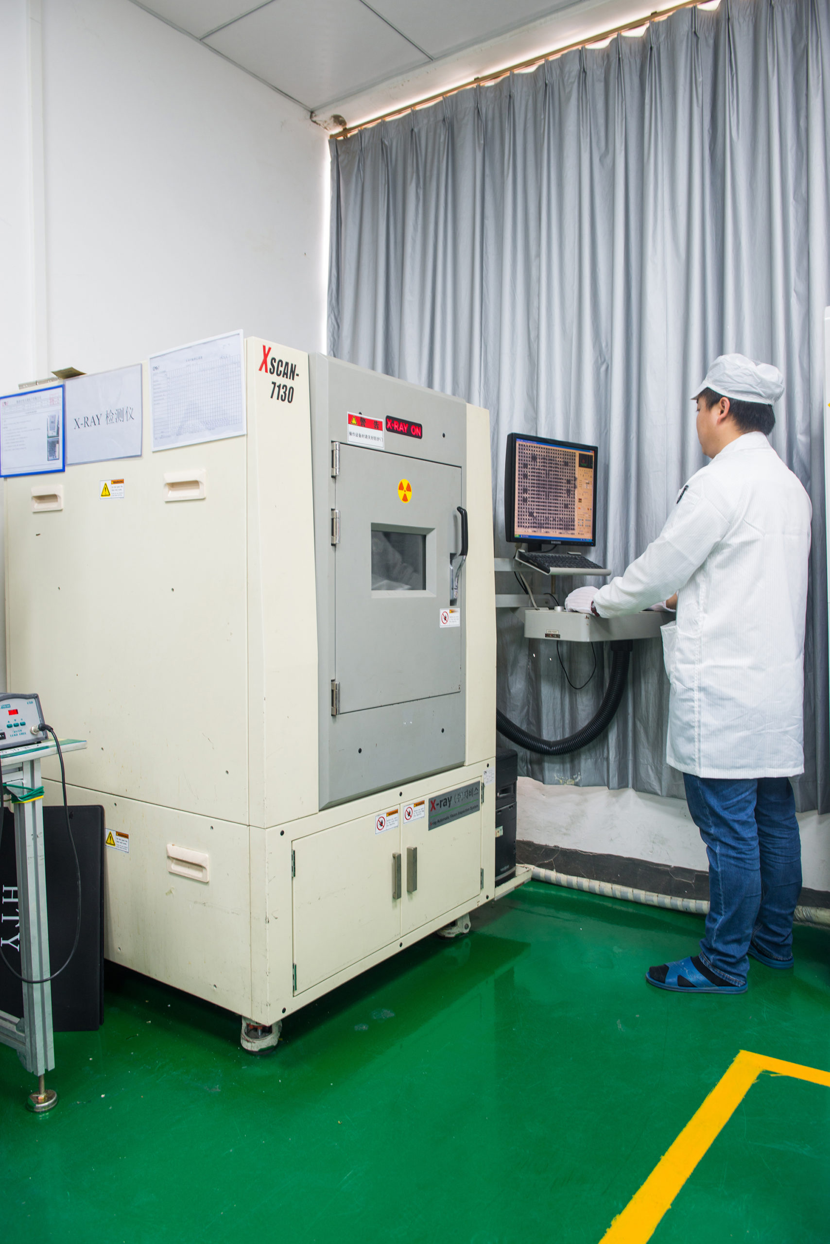
Using some of the latest machines and equipment, NextPCB provides two major services; PCB Manufacturing and PCB Assembly.
X-ray BGA Checking at NextPCB
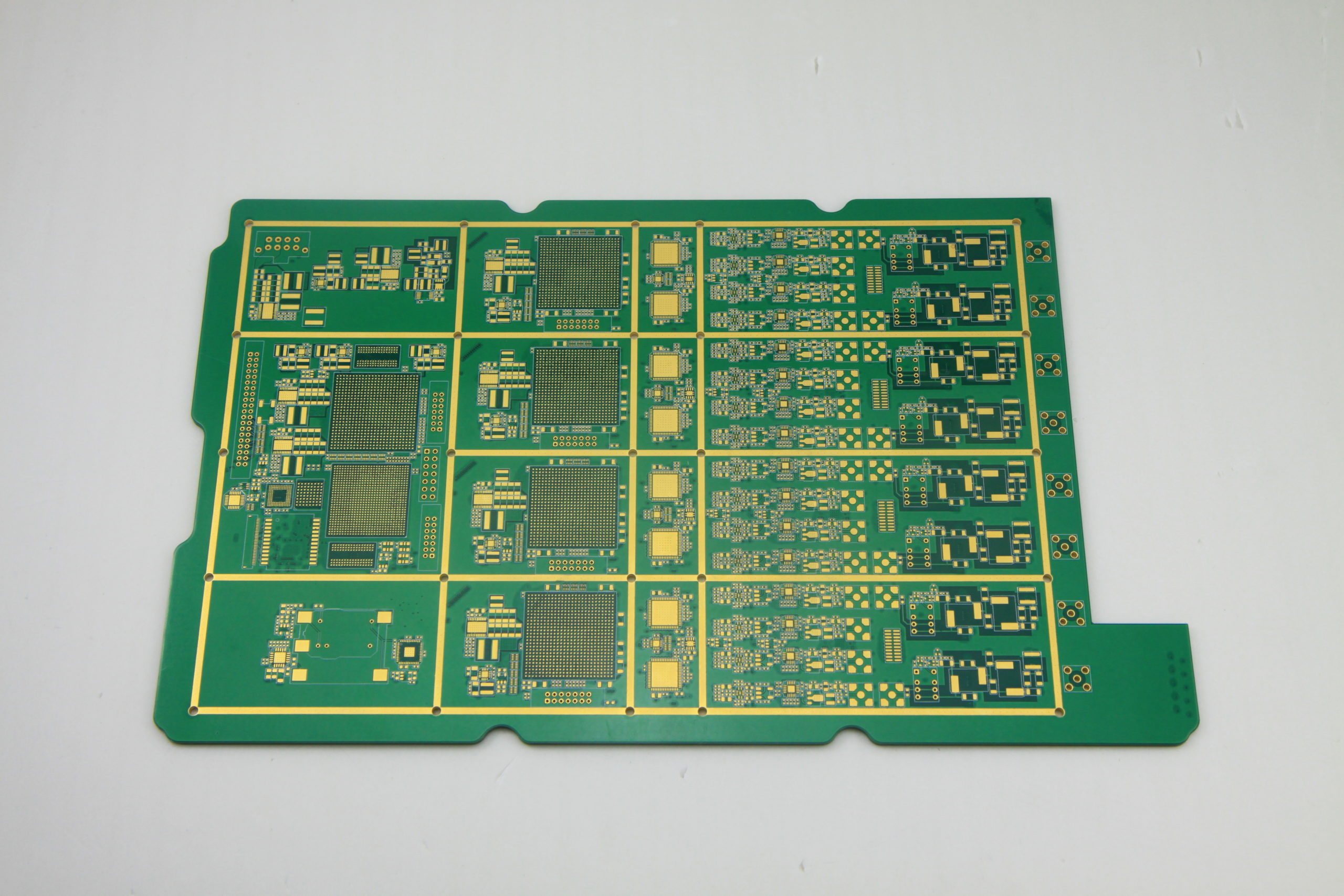
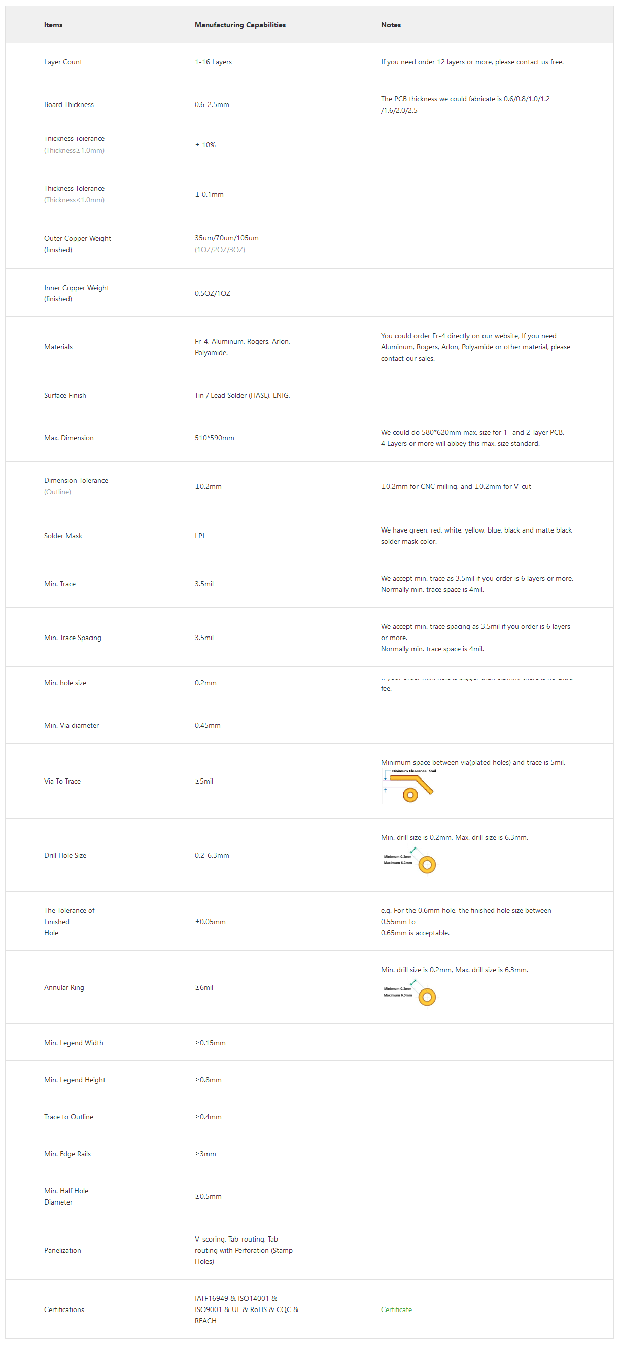
Their PCB manufacturing services cover both PCB prototyping and Mass production with lead time as fast as 24hours and costs as low as 0$. They are capable of manufacturing up to 16 layers of PCB with a thickness of up to 2.5mm. All their PCBs are UL and ROHS certified which reduces the number of certifications the product companies need to go through.
A summary of the Key capabilities of NextPCB as regards printed circuit board manufacturing is provided in the table below. They created the table to help customers determine if the capabilities of the equipment being used by NextPCB match the requirements of their design, and to also serve as a tool to help NextPCB’s regular customers design their PCBs to match the capacity of the company.
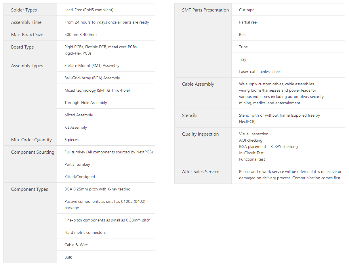
For PCB Assembly, NextPCB provides a turnkey experience with services like;
Components/parts Sourcing
PCB Fabrication
Pick and Place Machine based board population
SMT & Through-hole assembly with wave soldering
100% E-test and functional testing support
Worldwide free delivery with up to 30% off on the freight
A summary of some of the capabilities of NextPCB along the lines of PCB Assembly is provided in the table below;
For capabilities not listed in the table above, NextPCB works with the customer to ensure they are delivered.
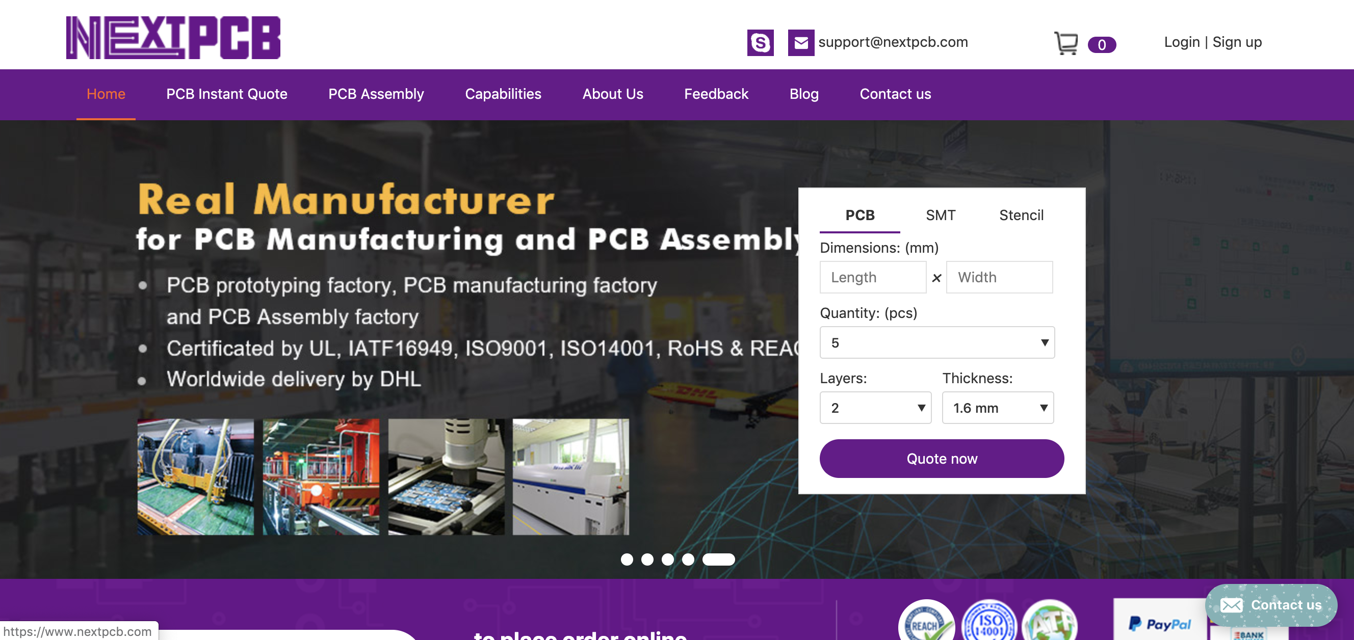
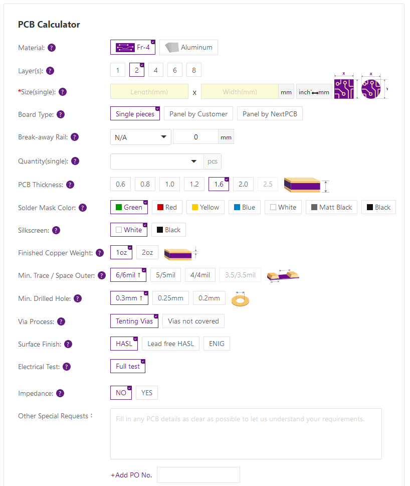
NextPCB Quote form
To make access to these services easy, NextPCBhas an online and instant PCB quote generator to which users can upload their Gerber files, and instantly get an evaluation of the design with a quote for its production. This makes it easy for developers to place orders for their boards from the comfort of their computers, and for situations that involve building a relationship with the company, NextPCB has a dedicated line through which customers can reach the company via their customer service professionals.
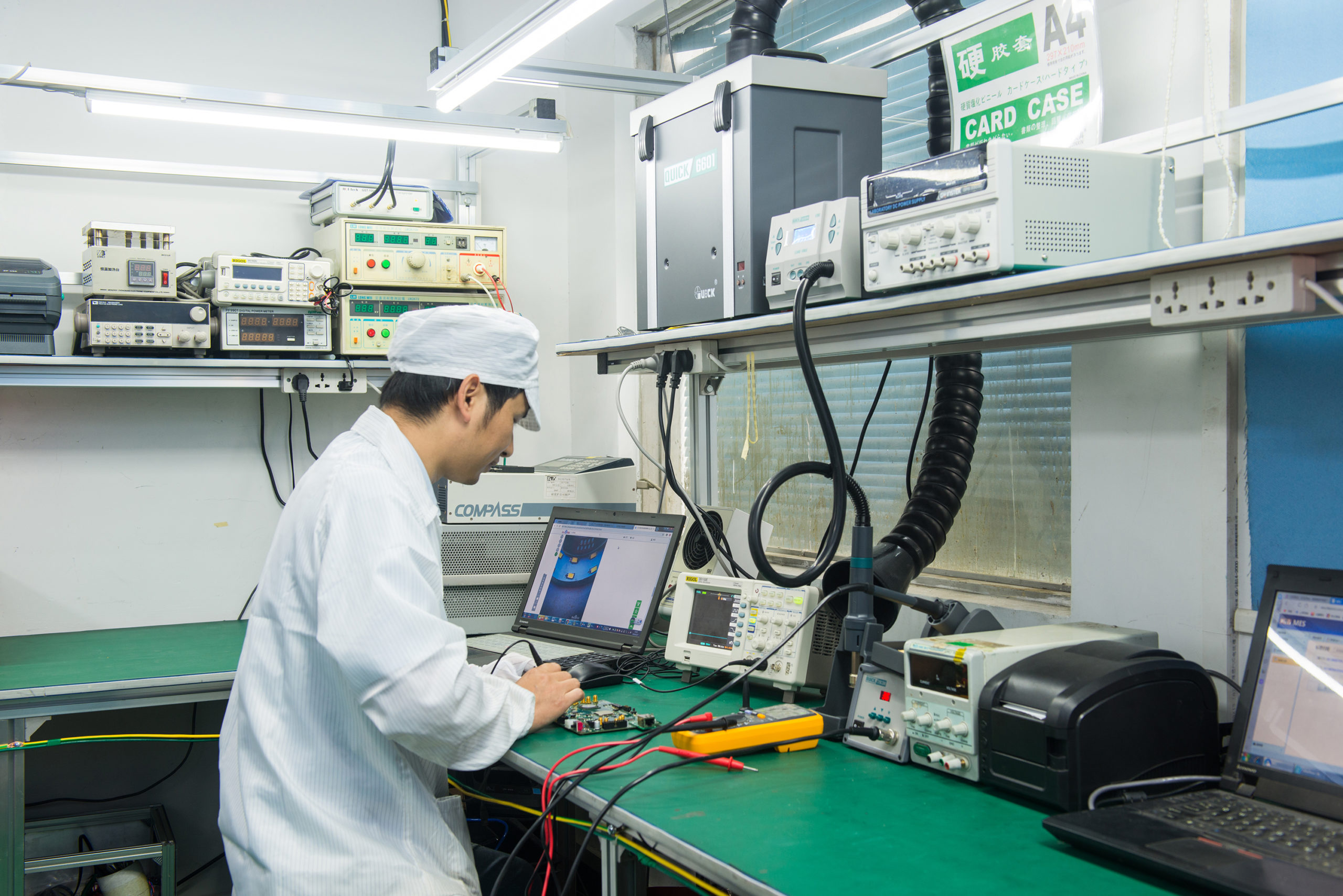
Functional Repair
NextPCB works to provide customers with reliable and flexible services, and one of the ways they do that is by providing customers with flexible payment and delivery options. NextPCB allows payment through channels like PayPal, Western Union, and ordinary bank transfer, while shipping and fulfillment are done via international logistics companies like DHL, FedEx, and the Singapore Post amongst others.
With an understanding of the big role the community plays, NextPCB is a big supporter of the open-source EDA community, supporting different community programs, and making donations to different community projects, including the widely popular KiCad for which NextPCB is regarded as one of the Main Sponsors.
NextPCB Drilling
Overall, compared with a number of PCB companies on the internet, the fact that NextPCBactually owns their factory (Not a Broker) and has been in the business for over 15 years means it will definitely be better to have them as partners for your projects, especially when for projects that require some level of experience in its manufacturing. Also, the parts sourcing services they provide help take a lot of burden off product companies as they will definitely have a wider reach and be able to help you get components that may be difficult to come by on the open market.