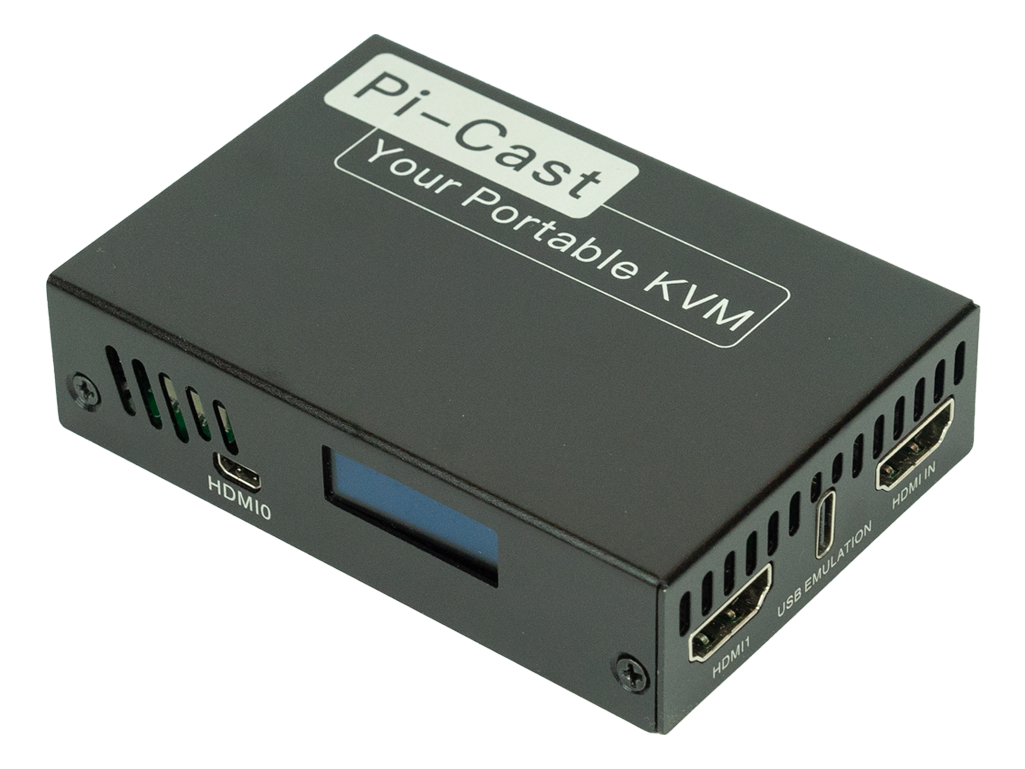
Powered by PYKVM, Pi-Cast KVM is a Raspberry Pi CM4-based KVM (Keyboard, Video, Mouse) solution that enables users to control and manage multiple devices remotely regardless of operating systems.
The device can also control connected devices remotely, through the web browser interface the only requirement is that the HDMI and USB should be connected to the KVM. It also has low-level device access, meaning you can configure the BIOS and UEFI settings even if there is no operating system, you can also power on/off and diagnose the target device only through web browser access.
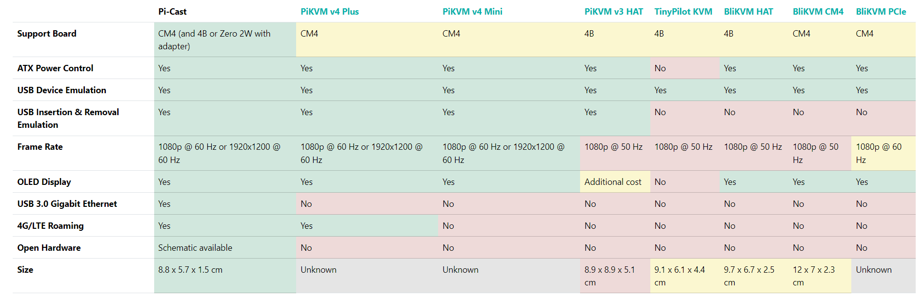
Pi-Cast offers five different versions, including a base model. The upgraded versions come with one of three expansion modules: the Ethernet/ATX/Console HAT, the USB 3.0 & M.2 B-key module, or the dual-ATX multiport switch. These enhanced versions are housed in a custom enclosure that includes the Pi-Cast KVM board. Furthermore, two additional models combine USB 3.0 & M.2 B-key functionality with the Ethernet/ATX/Console and dual-ATX variants.
The Pi-Cast KVM base model is equipped with the following specifications:
Support Board: Compatible with CM4 (and 4B or Zero 2W with an adapter).
Supported Resolution: Up to 1920×1080 resolution at 60Hz.
Video Input: 1x HDMI input utilizing the MIPI CSI-2 interface on the Raspberry Pi CM4.
Video Output: Dual HDMI outputs.
Storage: Includes an SD card slot (for CM4 Lite).
Networking: USB 3.0 Gigabit Ethernet for high-speed connectivity.
USB Ports: USB 2.0 Type-C serves as both client and host, along with a USB Device Emulation Port for keyboards, mice, and mass storage.
LED Indicators: Features indicators for CM4 activity, CM4 power, and Ethernet activity.
Miscellaneous Features: 40-pin GPIO header, real-time clock, boot button, OLED display, DIP Config Switch, 5V PWM fan connector, and an external antenna mount on the enclosure.
Power Supply: Utilizes USB Type-C for efficient power delivery.
Dimensions: Compact size measuring 86 x 56 x 15 mm.
Weight: To be determined (TBD).
The developers of this KVM made the project completely open-sourced, so the hardware and the software will be available on their GitHub repository. But when writing this article, only the hardware schematic is available in a PDF format.
The base model of the Pi-Cast KVM is priced at $199 with free worldwide shipping. The device will come preassembled with an RPI-CM4 module fan, enclosure, and every other necessary accessory. If you are interested in this project you can find more details about the device on the Crowd Supply page.
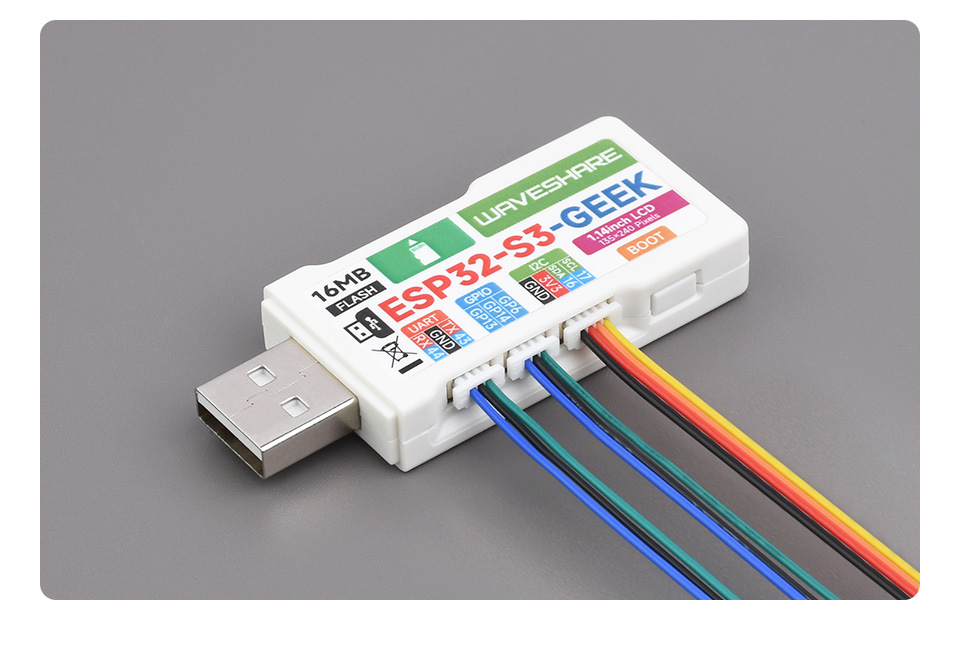
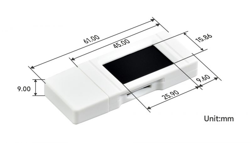
The Waveshare introduces ESP32-S3 GEEK, a small and versatile device designed for developers and hobbyists. It looks like a USB Flash drive and has a tiny 1.14-inch LCD for interaction.
Inside, it has a powerful ESP32-S3R2 chip with a 32-bit LX7 dual-core processor at 240 MHz. It comes with 512KB SRAM (for temporary storage), 384KB ROM (for permanent storage), 2MB PSRAM (for additional memory), and 16MB Flash memory (for storing programs and data).
This product stands out because it comes with a 1.14-inch IPS LCD, showing images in 240×135 pixels with 65,000 colors. It also supports both 2.4GHz Wi-Fi and Bluetooth Low Energy, making it suitable for a variety of IoT (Internet of Things) applications.
The board has several interfaces, including a USB-A port, UART port, GPIO header, and I2C port, which make it easy to connect and communicate with other devices. Moreover, it has a MicroSD card slot for adding extra storage space.
The ESP32-S3-GEEK is a development board created by Waveshare, and designed for tech enthusiasts. It features a USB-A port, a 1.14-inch LCD screen, a TF card slot, and various other peripherals. This board supports 2.4GHz WiFi and Bluetooth Low Energy 5, and it comes with integrated 16MB Flash memory and 2MB PSRAM. It also provides an I2C port, UART port, and GPIO header, offering flexibility for your projects.
ESP32-GEEK-DIMENSIONS
Key Features:
Powered by the ESP32-S3R2 chip with a 32-bit LX7 dual-core processor running at 240 MHz.
Includes 512KB SRAM, 384KB ROM, 2MB on-chip PSRAM, and onboard 16MB Flash memory.
Features a built-in 1.14-inch IPS LCD display with a resolution of 240×135 pixels and 65,000 colors.
Supports 2.4GHz WiFi and Bluetooth Low Energy wireless communication.
WiFi supports different modes, including Infrastructure BSS in Station, SoftAP, and Station + SoftAP.
WiFi operates in 1T1R mode with a data rate of up to 150 Mbps.
Bluetooth supports a high-power mode (20dBm).
Internal co-existence mechanism enables Wi-Fi and Bluetooth to share the same antenna.
Includes onboard 3PIN UART port, 3PIN GPIO header, and 4PIN I2C port for easy interfacing.
Comes with a plastic case and cables for added convenience.
Provides online open-source demos and resources, making it easier for learning and development.
ESP32-S3 GEEK is available on the product page for an affordable price of $12.99. You can get more information about the product on their wiki page
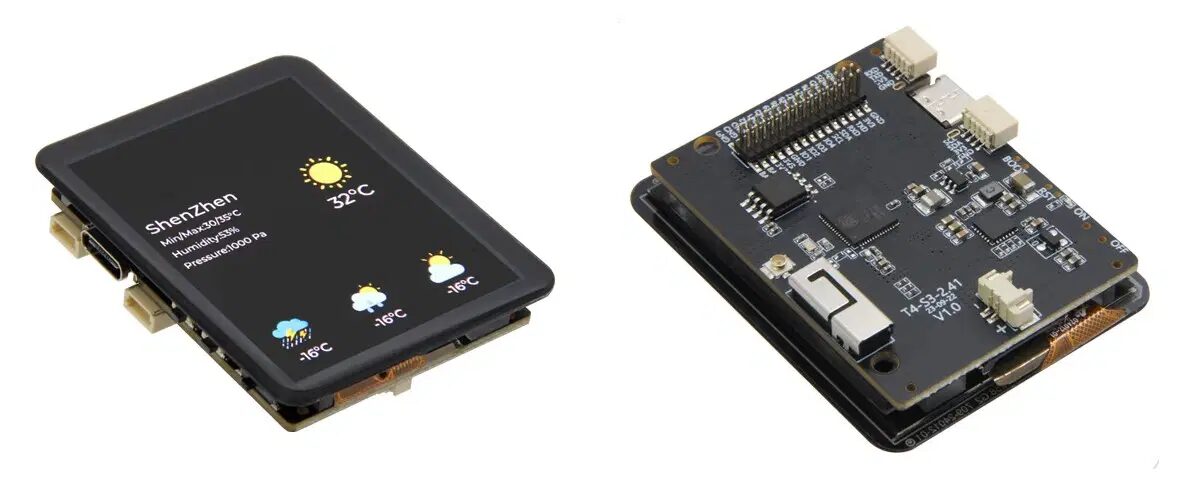
LILYGO, a specialist in embedded electronics, has recently introduced a compact development board featuring a touch-screen centered on the Espressif ESP32-S3. This new offering is called the LILYGO T4 S3 and comes with a 2.41″ full-color AMOLED display.
The recently launched development board is centered on Espressif’s ESP32-S3 system-on-chip. This means it incorporates a dual-core 32-bit Tensilica Xtensa LX7 microcontroller that operates at speeds of up to 240MHz, featuring vector instructions for enhanced performance in on-device machine learning and artificial intelligence (ML and AI) tasks. The board also includes 8MB of off-chip pseudo-static RAM (PSRAM).
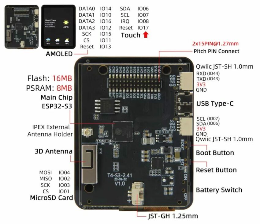
T4-S3-pinout-diagram
Additionally, the board offers 16MB of flash storage, with the option for microSD expansion. It features a 3D antenna and an IPEX connector designed for an external antenna. This single antenna serves the onboard Wi-Fi 4 and Bluetooth 5.0 Low-Energy (BLE) radios. Furthermore, the board is equipped with a USB Type-C port, serving dual power supply and programming purposes.
The standout feature of the board’s design is its prominent full-color display on the front. Utilizing active-matrix organic light-emitting diode (AMOLED) technology, the display boasts a resolution of 600×450 and a brightness of 800cd/m². Notably, it is fully touch-sensitive and communicates with the host microcontroller through a quad-SPI bus.
In terms of connectivity, the device includes two Qwiic ports for external hardware, a 30-pin 1.27mm-pitch header that exposes general-purpose input/output (GPIO) and power pins, and a JST-GH connector for an optional battery. Officially, the board supports development in PlatformIO, the Arduino IDE, and MicroPython. Unofficially, it should be compatible with any software running on the Espressif ESP32-S3, as long as suitable driver libraries for the display are available.
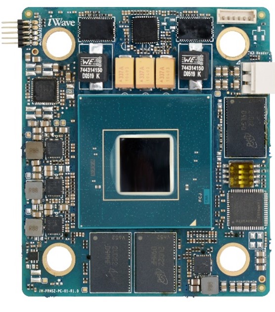
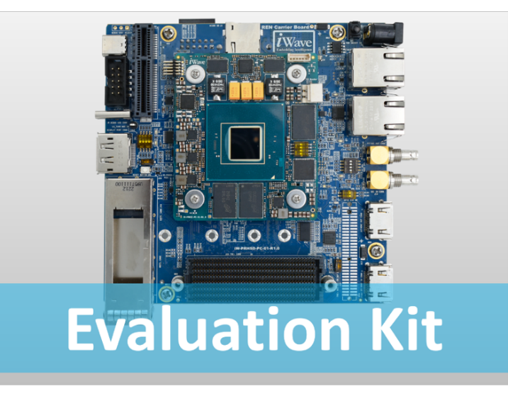
iWave is excited to announce the launch of the iW-RainboW-G58M System on Module (SoM), powered by the Intel Agilex® 5 FPGA Series that extends the innovations of the Intel Agilex® FPGA portfolio to midrange FPGA applications. The Agilex® 5 SoM is built in a compact form factor of 60mm x 70 mm and is compatible with the Intel Agilex® 5 FPGA and SoC E-Series family and B32A package in two device variants:
Group A: A5E 065A/052A/043A/028A/013A SoC FPGA
Group B: A5E 065B/052B/043B/028B/013B/008B SoC FPGA
The Agilex® 5 System on Module is an ideal building block for equipment used in wireless communications, video/broadcast, and industrial test and measurement sectors. The SoM supports 24 transceivers up to 28 Gbps, a PCIe Gen 4 connectivity interface, and a 2.5 Gigabit Ethernet PHY transceiver. iWave is now shipping early samples of the Agilex® 5 System on Module and evaluation kit, which comes with complete user documentation, software drivers, and a board support package.
Intel Agilex® 5 FPGAs and SoCs enhanced the industry’s first AI tensor block from Intel’s previous AI-optimized FPGA for general purpose, mid-range FPGAs in Intel Agilex® 5 FPGAs, making them an ideal choice for edge AI applications. The Agilex® 5 FPGA features an asymmetric applications processor system consisting of dual Arm Cortex-A76 cores and dual Cortex-A55 cores that optimize the performance and power efficiency of their workloads.
Highlights of iW-RainboW-G58M:
Agilex® 5 E- Series family with B32A Package
Dual-core 64-bit Arm Cortex-A76 up to 1.8 GHz
Dual-core 64-bit Arm Cortex-A55 up to 1.5 GHz
Up to 656K Logic cells
32Bit 4GB LPDDR4 for HPS
Dual 32Bit 4GB LPDDR4 for FPGA
32GB eMMC (Expandable)
1Gb QSPI Configuration flash
Up to 2.5G Ethernet
24 x transceivers up to 28Gbps
FPGA HSIO (Up to 48LVDS/96SE)
FPGA HVIO (Up to 100)
Compact Form Factor: 60mm x 70mm
Industrial-grade support
“Exciting to see the launch of the Intel Agilex® 5 FPGA, which extends the innovations of the Intel Agilex® FPGA portfolio to midrange FPGA applications, delivering high-efficiency AI and DSP functionality.” said Immanuel Rathinam, Vice President – System on Modules at iWave. “The Intel Agilex® 5 FPGA powered System on Module provides an optimal balance in performance and power for advanced image processing, 5G wired/wireless, and edge AI applications while accelerating customers’ time to market with reduced complexity and risk.”
“We are thrilled to see one of our long-term partners, iWave, become early adopters of the Intel Agilex 5 E-Series FPGA devices,” said Deepali Trehan, Vice President, DCAI General Manager, Marketing, Product and Programs Group. “With 1.6x better total performance per watt on the Agilex 5 E-Series compared to competing 16nm-based FPGAs, iWave iW-Rainbow-G58M System-on-Module (SoM) and carrier board provides rich features and flexibility to help our mutual customers develop their end solutions quickly and attain business success.”
iWave provides their customers with an evaluation kit with the latest software packages to expedite their evaluation and time to market.
The evaluation kit supports the following connectors and interfaces:
5G Ethernet RJ45 MagJack
Gigabit Ethernet RJ45 MagJack
PCIe Gen4 x4
20-Pin PS Header: UART, SPI, GPIOs
0 + USB2.0 through Type-C
DP (2 lane)
FMC+, PMOD & QSFP+ Connector
HDMI OUT/IN & SDI IN/OUT
Type-C USB connector for USB and JTAG
JTAG Connector
Click here for more details on the System on Module and Evaluation Kit.
iWave maintains a product longevity program that ensures the System on Modules are available for long periods of time (10+ years). iWave offers customers extensive technical support during the evaluation and product development phase, alongside ODM Design services such as carrier card design, thermal simulation, and ODM as a business model.
iWave is an embedded systems engineering and solutions company, designing solutions for the Industrial, Medical, Automotive, and Avionics vertical markets. Building on a core competency of embedded expertise since 1999, iWave boasts of an extensive portfolio of high-performance FPGA and SoC FPGA System on Modules and embedded computing platforms enabling customers in their product development journey. Learn more about iWave at www.iwavesystems.com.
The R-2R Digital-to-Analogue Converter is a type of data converter that transforms a digital binary number into an analog output signal that is proportionate to the value of the digital number using two precision resistors.
The binary-weighted digital-to-analog converter, in contrast to the R-2R DAC, produces an analog output voltage that is the weighted sum of the separate inputs. Because of this, the ladder network of this design necessitates a wide variety of precision resistors, rendering it both costly and unfeasible for most DACs that require lower resolution levels.
Given that the binary-weighted DAC is built upon a summing amplifier topology-based closed-loop inverting operational amplifier, this kind of data converter design would be suitable for a D/A converter with a few bits of resolution. However, building an R-2R digital-to-analog converter with an R-2R resistive ladder network is a far easier method that only needs two precise resistances.
There are just two resistive values used in the R-2R resistive ladder network. No matter how many bits are used to create the ladder network, the first resistor has the base value “R,” and the second resistor has twice the value of the first resistor, or “2R.”
For instance, because the base resistor “R” is not particularly important, we may just use a conventional 1kΩ resistor for it, and a 2kΩ resistor for “2R” (or multiples of it). As a result, 2R’s resistive value will always be twice that of the base resistor, R. In other words, 2R = 2*R. This indicates that, in comparison to the prior weighted resistor DAC, it is considerably simpler for us to maintain the necessary precision of the resistors along the ladder network. However, what exactly is an “R-2R resistive ladder network”?
R-2R Resistive Ladder Network
The “ladder” descriptor derives, as its name suggests, from the resistors employed in the network being arranged in a ladder-like fashion. A straightforward method of transforming digital voltage signals into an equivalent analog output is to use an R-2R resistive ladder network.
The ladder network receives input voltages at different places along its length; the more input points, the higher the R-2R ladder’s resolution. The output signal obtained from all these input voltage points is obtained from the ladder’s end and utilized to power an operational amplifier’s inverting input.
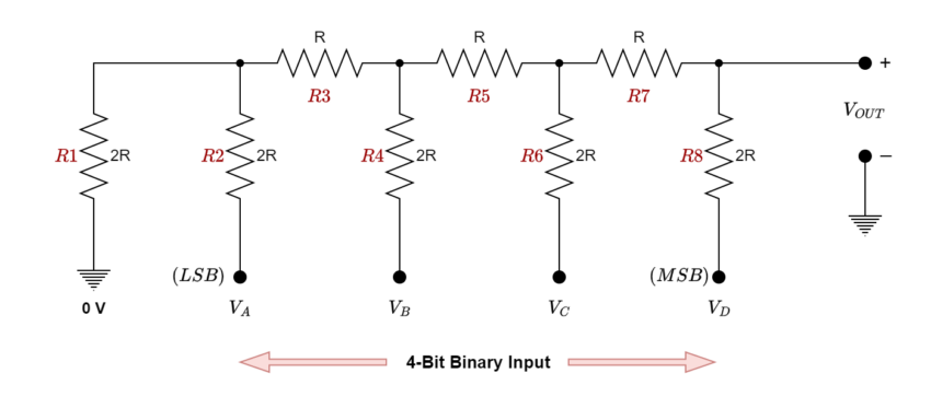
The output voltage of an R-2R resistive ladder network, thus, is solely dependent on the interaction between the input voltages. It is essentially just lengthy strings of parallel and series-linked resistors functioning as interconnected voltage dividers along their length. Examine the following simple 4-bit R-2R ladder network (4-bits due to its four input locations).
4-bit R-2R Resistive Ladder Network
Figure 1: 4-bit R-2R Resistive Ladder Network
Although this 4-bit resistive ladder circuit may appear complex, it just involves connecting resistors in series and parallel configurations and applying basic circuit rules to determine the output’s proportionate value by working backward to the input source. Assume that all the binary inputs VA=VB=VC=VD=0V i.e., grounded. Therefore, 0000 is the binary code that corresponds to these four inputs.
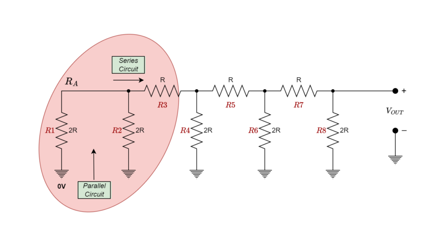
By starting from the left side and applying the concise formula for two parallel and series resistors, we can get the ladder network’s equivalent resistance as follows:
Figure 2: Calculating equivalent Resistive of Ladder Network
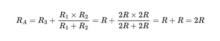
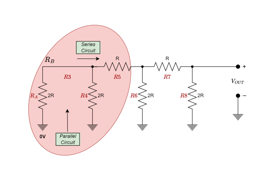
Resistors R1 and R2 are in “parallel” with each other but in “series” with resistor R3. The equivalent resistance of these three resistors may then be found; for ease of use, we’ll refer to it as RA.
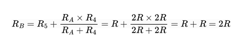
In such case, “2R =RA are equal. It is now clear that the equivalent resistance, denoted as “RA,” is parallel to R4 and in series with R5.
Figure 3: Calculating equivalent Resistive of Ladder Network
Once more, we may determine this combination’s equivalent resistance and refer to it as RB.
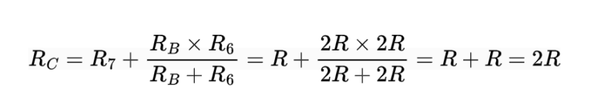
So, the equivalent resistance RC will be;
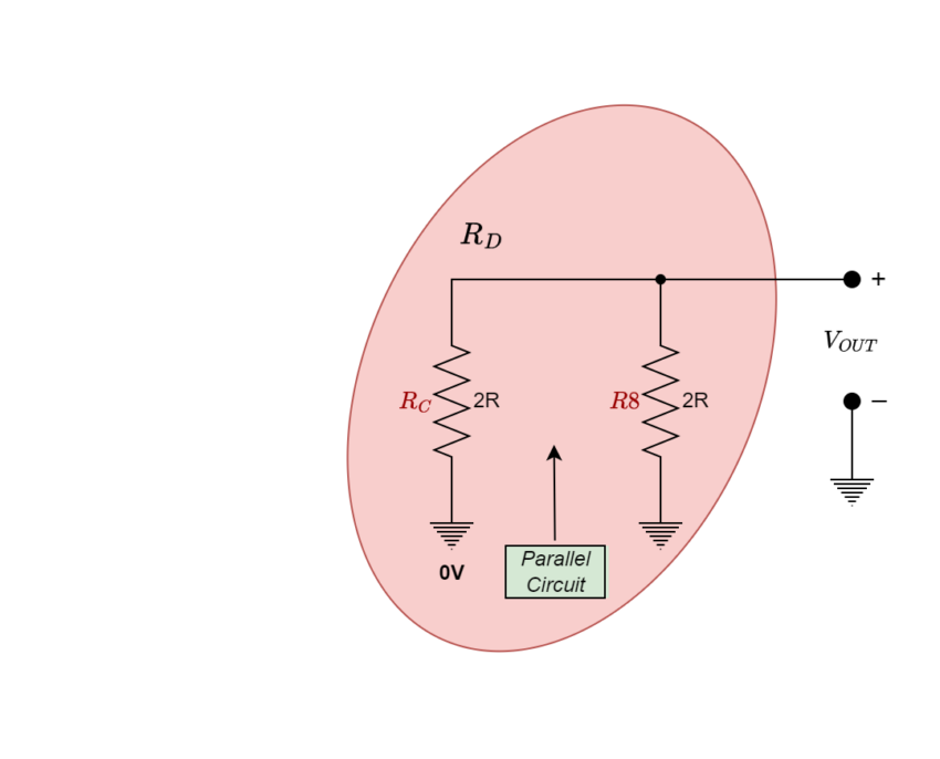
Once more, the resistor combination RC is equal to “2R,” which, as shown, is in parallel with R8.
Figure 4: Calculating equivalent Resistive of Ladder Network
As we’ve already seen, the outcome of two parallel resistors with identical values is ½, thus 2R in parallel with 2R equals an equivalent resistance of R. Therefore, when a binary code of “0000” is applied to its four inputs, the entire 4-bit R-2R resistive ladder network, which is made up of individual resistors coupled together in parallel and series combinations, has an equivalent resistance (REq) of “R.”
Consequently, our fundamental 4-bit R-2R digital-to-analog converter circuit would resemble this when applied with a binary code of “0000” as an input:
R-2R DAC Circuit with Four Zero (LOW) Inputs
Figure 5: R-2R DAC Circuit with Four Zero (LOW) Inputs
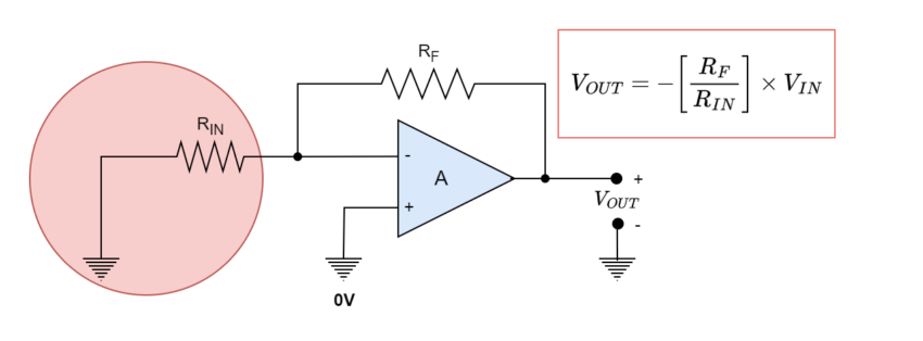
The formula for an inverting operational amplifier’s output voltage VOUT is given as (RF/RIN)*VIN. With RIN connected to ground (0V), there is no voltage value for input (VIN = 0), thus if we set RF equal to RIN (RF = RIN = 1), the output voltage would be (1/1)*0 = 0 volts. Thus, an analog output of 0 volts is produced by a 4-bit digital input of 0000 for a 4-bit R-2R DAC with four grounded inputs (LOW). As a result, the output voltage will be “zero” volts.
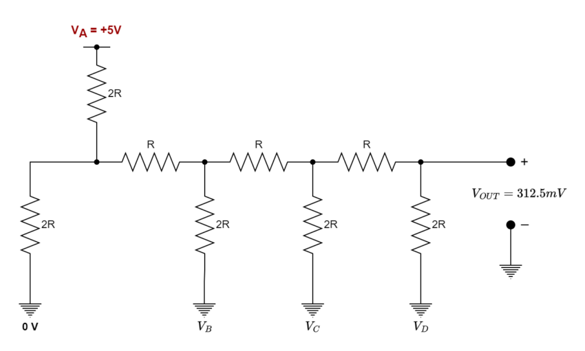
Now we will see, connecting input bit VA HIGH to +5 volts, how the output voltage of the op-amp is comparable to the resistive value of the R-2R ladder network.
R-2R DAC with Input VA
Figure 6: R-2R DAC with Input VA
As shown in the figure, VA input is HIGH and grounded at logic level “1,” whereas all other inputs are grounded at logic level “0.” Since the R-2R ladder network is a linear circuit, we can determine Thevenin’s equivalent resistance using the same parallel and series resistance computations as previously to determine the expected output voltage. Consequently, 312.5 milli-volts (312.5 mV) is determined as the output voltage or VOUT.
With a 4-bit R-2R resistive ladder network, this 312.5 mV voltage shift is categorized as the Least Significant Bit (LSB) as it is one-sixteenth the value of the +5V input voltage (5/0.3125 = 16). As the least important bit, input VA will therefore establish the “resolution” of our straightforward 4-bit digital-to-analog converter as the smallest voltage shift in the analog output is equivalent to a single-step change in the digital inputs. Therefore, 312.5mV (1/16th) for a +5V input will be the value for our 4-bit DAC.
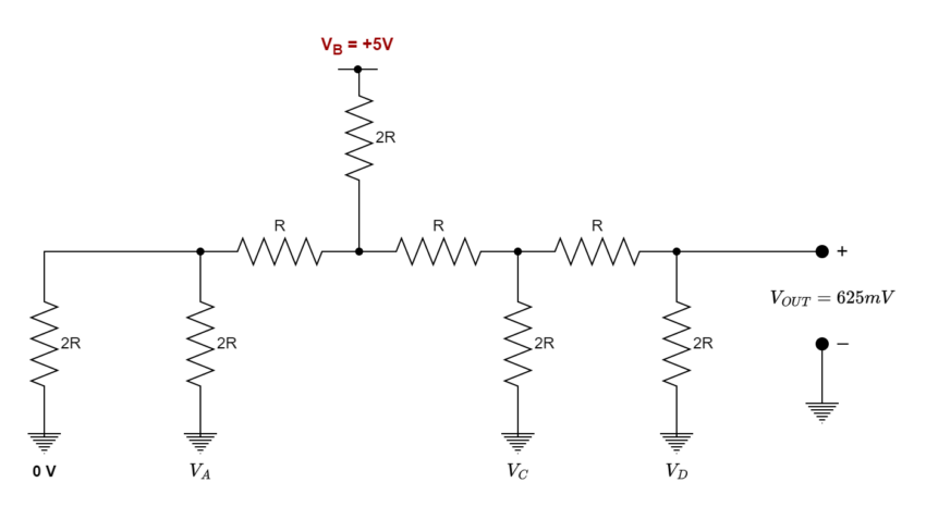
As we connect the input bit VB HIGH to +5 volts, let’s examine what happens to the output voltage.
R-2R DAC with Input VB
Figure 7: R-2R DAC with Input VB
The output voltage, VOUT, is determined to be 625mV, or one-eighth (1/8th) of the value of the +5V input voltage (5/0.625 = 8) with input VB HIGH and logic level “1” and all other inputs grounded at logic level “0.” Additionally, we observe that the output voltage doubles when only the input bit VA is applied. This is to be expected because the input bit is the second bit and has twice the weighting of the first bit.
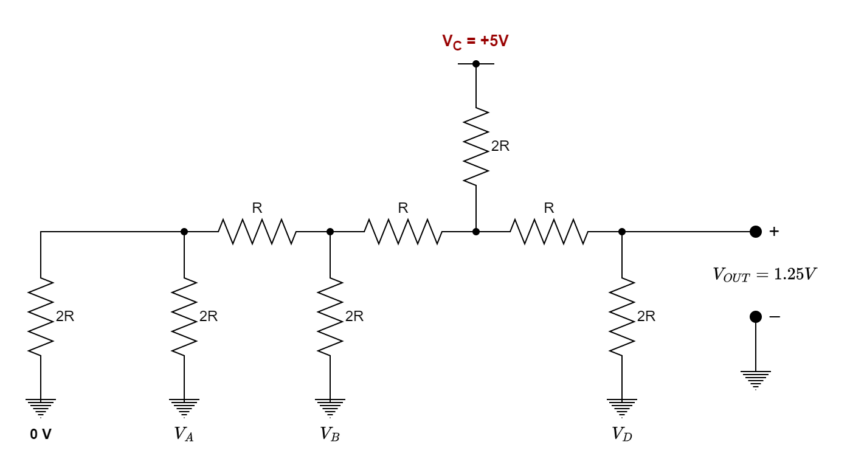
Let’s now examine the effects of connecting input bit VC HIGH to +5 volts on the output voltage.
R-2R DAC with Input VC
Figure 8: R-2R DAC with Input VC
One-quarter (1/4) of the value of the +5V input voltage (5/1.25 = 4) is the output voltage or 1.25 volts when input VC is HIGH, logic level “1” is used, while the remaining input bits are at logic level “0.” Once more, we can observe that this voltage is four times the value of bit VA and double the output of input bit VB. This is because the weighting of input VC, which is the third bit, is double that of the second bit and four times that of the first bit.
Lastly, let’s see what happens to the output voltage when input VD is HIGH, i.e., connected to +5 volts.
R-2R DAC with Input VD
Figure 9: R-2R DAC with Input VD
The output voltage, VOUT, is determined to be 2.5 volts when input VD is HIGH, logic level “1” is used, and all other inputs are at logic level “0.” This is one-half (1/2) of the +5V input voltage (5/2.5 = 2). Once more, we can see that because this voltage is the fourth bit and is therefore categorized as the Most Significant Bit (MSB), it is twice the output of input bit VC, four times the value of bit VB, and eight times the value of input bit VA.
Then, we can observe that, given that input VA controls the DAC’s resolution because it represents the LSB, input VB is double to VA, input VC is four times greater than VA, and input VD is eight times greater than VA, we can use the following equation to determine the relationship between the analog output voltage of our 4-bit digital-to-analog converter.
Digital-to-Analogue Output Voltage Equation
Where the 16 (24) potential combinations of inputs to the 4-bit R-2R ladder network of the DAC are represented by the denominator number of 16.
Since each input bit’s weighting is always based on the least significant bit (LSB), we may extend this equation further to get a generalized R-2R DAC equation for any number of digital inputs for an R-2R D/A converter. This gives us a generalized equation of:
Where “n” is the number of digital inputs in the DAC’s R-2R resistive ladder network, which results in the resolution VLSB = VIN/2n.
Thus, it is evident that input bit VA when HIGH will result in the least amount of output voltage change, while input bit VD when HIGH will result in the most amount of output voltage change. Therefore, the predicted output voltage is determined by adding together the effects of each HIGH-connected input bit.
Since each input will have a step increase equal to the LSB, the ladder network should ideally result in a linear relationship between the input voltages and the analog output. To this end, we can create a table of expected output voltage values for all 16 possible combinations of the four inputs, with +5V denoting a logic “1” condition as demonstrated.
4-bit R-2R D/A Converter Voltage Output
Figure 10: 4-bit R-2R D/A Converter Voltage Output
The full-scale analog output voltage for a binary code of 1111, as you may have noted, is always smaller by the equivalent of one LSB bit (312.5mV in our case), and it never reaches the same value as the digital input voltage (+5V).
On the other hand, the analog output voltage approaches full-scale when all input bits are HIGH. Similarly, when all the input bits are LOW, VOUT approaches 0 volts.
R-2R Digital-to-Analogue Converter
Since we know the characteristics and operations of the R-2R resistive ladder network, we can use it to create an R-2R digital-to-analog converter. We can construct a straightforward R-2R digital-to-analog converter like the following by utilizing our 4-bit R-2R resistive ladder network and attaching it to an inverting operational amplifier circuit:
Figure 11: R-2R Digital-to-Analogue Converter
A combinational or sequential logic circuit, a data register, a counter, or even just switches can be utilized to create the digital logic circuit that powers the D/A converter. The application will determine how an R-2R D/A converter of “n” bits should be connected. Digital-to-analog converters are included in all-in-one boards like the Arduino and Raspberry Pi, which makes programming and interface considerably simpler. Numerous well-known DACs are available, including the 8-bit DAC0808.
R-2R D/A Converter Example:
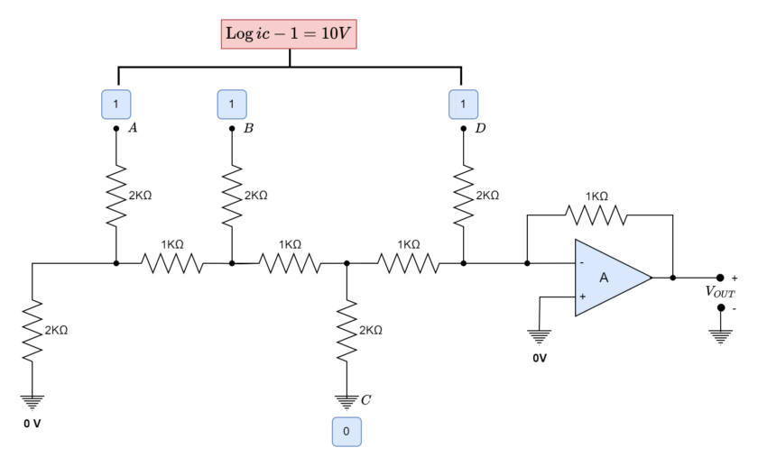
A 4-bit R-2R digital-to-analog converter is built to use the output from a digital logic circuit to regulate the speed of a small DC motor. Analyze the analog output voltage from the DAC when the input code is the hexadecimal number “B” if the logic circuit utilizes 10-volt CMOS devices.
The number eleven in decimal notation is equivalent to the hexadecimal character “B.” The binary code “1011” in binary is equivalent to the decimal number eleven. That is, 10112 = B16. Thus, bit D = 1, bit C = 0, bit B = 1, and bit A = 1 are the input bits for our 4-bit binary integer, 10112.
Assuming the feedback resistor (RF) to be equal to “R,” the circuit for our R-2R D/A converter will be as follows:
Figure 12: A R-2R D/A Example Converter
The R-2R network will receive an input voltage of 10 volts since the digital logic circuit employs 10-volt CMOS chips. Since this 4-bit ladder DAC also has 24 possible input permutations, the output voltage for a binary code of 10112 is determined using the equation above:
Hence, when the input code is 10112, the analog output voltage that is utilized to regulate the DC motor is computed as follows: -6.875 volts. Keep in mind that the operational amplifier’s inverted input is the reason the output voltage is negative.
The least significant bit (LSB), which is specified as follows, will have a resolution of equal to:
In this 4-bit R-2R digital-to-analog converter example, the smallest step change in the analog output voltage, or VOUT, is 0.625 volts for a 1-bit LSB change in the digital input. That is, rather than changing in a straight linear fashion, the output voltage varies in stages or increments of 0.625 volts.
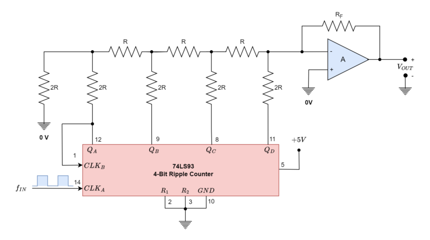
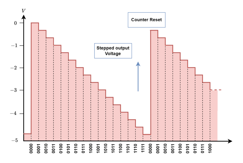
4-bit Binary Counting R-2R DAC
By now, perhaps, we should be able to construct an R-2R ladder DAC using just two resistor values: one is the base value “R,” and the other is twice that amount, or “2R.” With four input data lines, A, B, C, and D, we have created a 4-bit R-2R DAC in our straightforward example above. This gives us sixteen (24) distinct input possibilities, ranging from “0000” to “1111”.
There are several methods to create the binary code for these four digital input lines, including solid-state switches, microcontrollers, and digital circuits. Nevertheless, using a 4-bit binary counter like the 74LS93 is an intriguing alternative.
With the application of a single external clock signal, the 4-bit J-K ripple counter 74LS93 may be made to count from 00002 to 11112 (MOD-16) and reset back to zero (0000). Asynchronous and sometimes referred to as a “ripple” counter, the 74LS93 generates a 4-bit binary output because of internal J-K bistables responding to a clock or timing input.
The counters’ output lines divide the external clock’s frequency (or period) by a factor of 2, 4, 8, and 16 as the clock pulse ripples through the four J-K flip-flops to produce the necessary 4-bit output count sequence, which runs from 00002 to 11112.
Figure 13: 4-bit Binary Counting R-2R DAC
Observe that the external CLKB input needs to be linked to the QA (pin-12) output to count upward from 0000 to 1111, and that input CLKA (pin-14) needs to receive the input timing pulses.
This straightforward 4-bit asynchronous up counter uses the same counting sequence seen in the top table, which is based on the 74LS93 binary ripple counter. A clock pulse applied to the QA, QB, QC, and QD outputs causes a one-step change.
The operational amplifier’s input recognizes this step shift and, to the binary code at the R-2R ladder inputs, produces a negative voltage (inverting op-amp). Every step’s output voltage value will line up with the values shown in the above table.
The maximum negative output voltage of the digital-to-analog converter will be produced by the ripple counter counting in succession with the four outputs providing an output sequence of binary values up to the 15th clock pulse, at which point the outputs are set to 11112 (decimal 15).
The op-amp’s output is reset to zero volts on the sixteenth pulse, which also resets the counter’s output sequence and counts back to 0000. When the subsequent clock pulse is applied, a fresh counting cycle from zero to VOUT(max) is initiated.
The following time diagram displays the output sequence for this straightforward 4-bit binary asynchronous counting R-2R D/A converter.
4-bit R-2R DAC Timing Diagram
Figure 14: 4-bit R-2R DAC Timing Diagram
Therefore, it is evident that when the ripple counter counts from 00002 to 11112, respectively, the operational amplifier’s output voltage swings from zero volts to its maximum negative value. This straightforward circuit might be used to continuously change the speed of a DC motor from slow to fast and back again at a rate defined by the clock period, or it could be used to adjust the brightness of a light connected to the output of the op-amp.
This time, the R-2R DAC and ripple counter are set up for 4-bit operation. However, by utilizing widely accessible binary ripple counters, like the CMOS-4024 7-bit (÷128), CMOS-4040 12-bit (÷4096), or the larger CMOS-4060 14-bit (÷16,384) counter, and by including additional input resistors in the R-2R ladder network, like those offered by Bourne’s, the resolution (LSB) of the circuit can be significantly reduced, resulting in a smoother output signal from the R-2R digital-to-analog converter.
Conclusion
An R-2R Digital-to-Analogue Converter uses two precision resistors to transform a digital binary number into an analog output signal that is proportionate to the value of the digital number.
The mentioned generalized equation may be used to determine the output voltage of an R-2R digital-to-analog converter with any number of digital inputs; VO= (VA+2VB+4VC+8VD+16VE+32+VF…)/2n
The full-scale analog output voltage with a binary code of 1111 never reaches the same value as the digital input voltage and is always smaller by the equivalent of one LSB bit. Similarly, when all the input bits are LOW, the resulting lower resolution of LSB causes VOUT to approach 0 volts.
To make an R-2R digital-to-analog converter, an op-amp coupled with a 4-bit R-2R ladder network can be utilized. The output of a digital logic circuit is used to control a tiny DC motor’s speed.
Using a 4-bit binary counter with an op-amp, like the 74LS93 ripple counter, is an interesting alternative. It causes the operational amplifier’s output voltage to swing from zero volts to its maximum negative value when the ripple counter counts from 00002 to 11112, respectively.
The speed of a DC motor may be continually adjusted using 4-bit binary counter circuits, going from slow to fast and back again at a pace determined by the clock period. It may also be used to control the brightness of a light that is connected to the op-amp’s output.
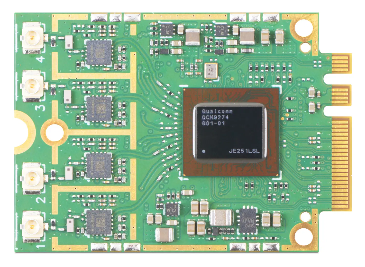
8devices has just announced a new WiFi 7 module with M.2 A+E-Key, the module is built on top of the QCN9274/QCN6274 chipsets and can achieve up to 11Gbps transfer rate in MIMIO or Split configurations. The device uses the FirmUX-embedded Linux OS as the interface.
The Noni modules can communicate on multiple frequencies simultaneously using Multi-Link Operation (MLO) and adaptive puncture interference to ensure performance in different environments. The QCN9274-based variants have additional features like Provisioned Multi-Link, Dense deployment, and Location and RF sensing.
Key Features and Specifications of Noni 56M2:
Models:
Noni 56M2-4×4-B
Noni 56M2-4×4
Noni 56M2-4×4-I
Chipset:
QCN-6274
QCN-9274
Form Factor:
M.2 A+E key
Frequency:
5.1 – 7.125 GHz
4.9 – 7.125 GHz
MiMo:
MU 4×4 or 2×2 + 2×2
Bandwidth:
20 – 320 MHz
Modulation:
4096 (4K) QAM
Multiplexing:
16 user DL/UL OFDMA
37 user DL/UL OFDMA
Data Rate:
11 Gbps+
Number of Clients:
256 (Noni 56M2-4×4-B)
512 (Noni 56M2-4×4)
Multi-Link Operation (MLO):
Yes
Interference Puncturing:
Static (Noni 56M2-4×4-B)
Static and Dynamic (Noni 56M2-4×4-I)
Advanced Software Features:
No (unless obtaining licensed binary packages from Qualcomm)
Provisioned Multi-Link, Dense Deployment, Location and RF Sensing
Temperature Range:
0°C to +85°C (Noni 56M2-4×4-B)
-40°C to +85°C (Noni 56M2-4×4-I)
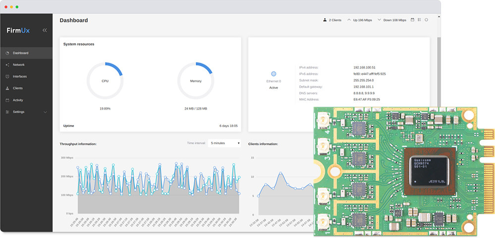
Noni modules use FirmUX Linux with open or Qualcomm drivers. It has WPA3 security, a user-friendly dashboard, Wireguard VPN, and boasts a 34% improvement over past boards with OpenWrt.
FirmUx Basic offers free AP, router, and bridge functions, but the ‘Standard’ and ‘Premium’ versions add features like a responsive UI, dual boot, mesh networking, and UI rebranding. FirmUX source code is open, and downloadable for premium customers. The company sells the Noni WiFi 7 module for $74 to $85 on its online store, you can check out its product page for more details.
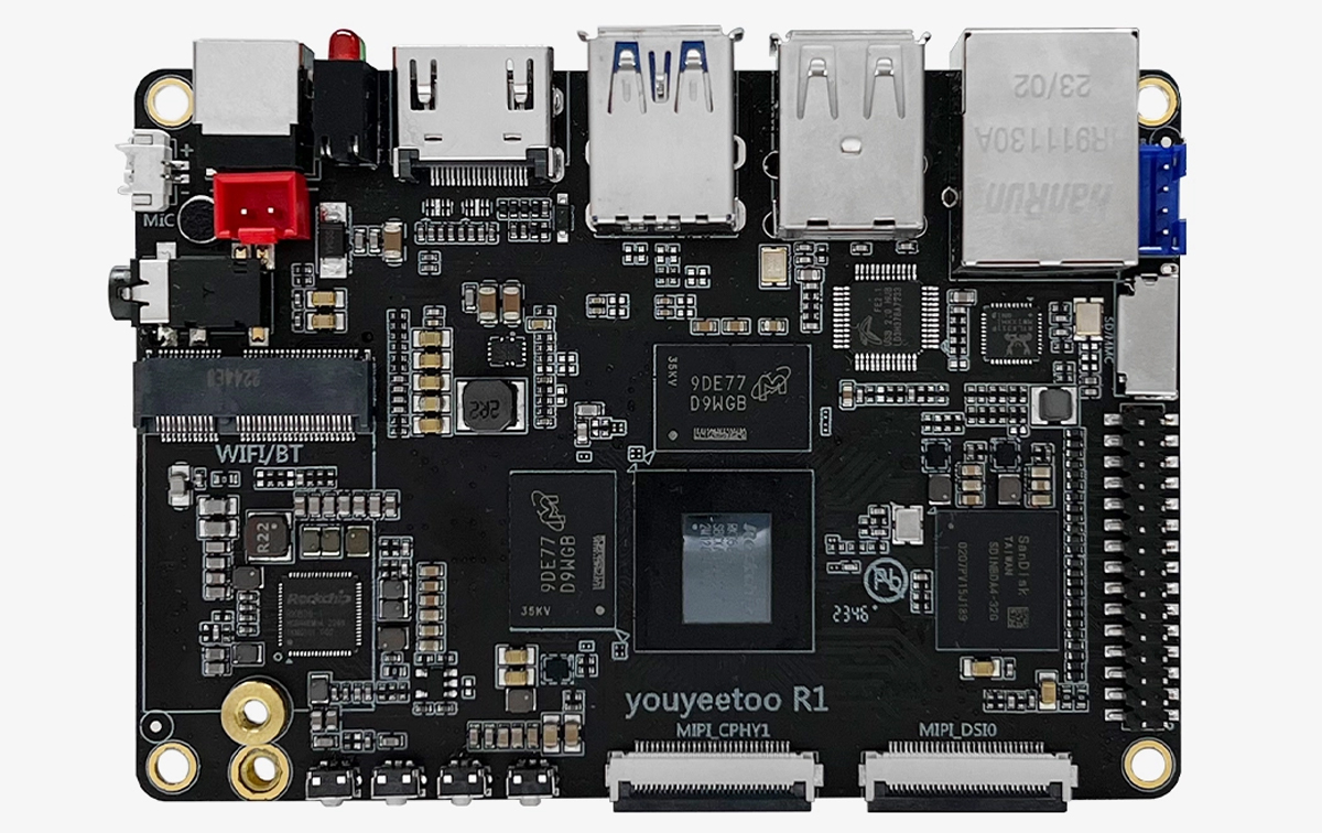
Youteetoo has just released the Youteetoo Cyboboard R1 or in short Youyeetoo R1, it is a Rockchip RK3588S-based SBC in a 100×69.3mm form factor. The board is tiny but packs a boatload of features including two M.2 ports, WiFi and Bluetooth connector, NFC, four display interfaces, dual MIPI CSI interfaces, and many other features.
Additionally, the board includes up to 32GB RAM, 256GB eMMC, gigabit Ethernet, five USB ports, a built-in microphone, various audio I/O, a 30-pin expansion header, and more.
In terms of software, the board supports Android 13, Debian 11, Ubuntu 22.04, and Buildroot, all on Linux 5.10. But at the time of writing this post, the wiki page is still in progress.
One unique feature of this board is that it has built-in NFC module. But I am not sure how useful the NFC might be, because you can always buy an NFC module that will cost you a few dollars.
The SBC doesn’t have a heat sink, but the company later released a heatsink that can be found in the Aliexpress store with 3M thermals.
Youyeetoo R1 specifications:
SoC: Rockchip RK3588S
CPU: Octa-core with 4x Cortex-A76 cores @ up to 2.2-2.4 GHz, 4x Cortex-A55 cores @ up to 1.8 GHz
Video Output: HDMI 2.1 up to 8Kp60, MIPI DSI, USB Type-C with DP1.4
Video Input: 2x MIPI CSI, optional HDMI input
Audio: 3.5mm jack, HDMI, on-board microphone
Networking: Gigabit Ethernet, M.2 WiFi 5/6 & Bluetooth 5.0/5.2, NFC
USB: 1x USB 3.0, 2x USB 2.0, 1x USB 3.1 OTG Type-C
Expansion: M.2 sockets for SSD/LTE, GPIO header, Debug UART
Misc: Power/Recovery/Reset/Boot buttons, user LEDs, RTC battery connector, fan connector
Power Supply: 12V/3A via DC jack or 2-pin socket
Dimensions: 100 x 69.3 mm
Youyeetoo’s R1 SBC is priced at $109 for the (4GB/32GB) version on Aliexpress, but you can buy it from their official store for $99. At the time of writing this article, I only found the 4/32 is available for purchase, but the other top configurations like the 8GB/64GB, with 16GB/128GB and 32GB/256GB models are not currently for sale.
65W CPU support, purpose-built power input architecture, and unparalleled expansion make the EPIC-RPS9 the industrial solution for 2024
AAEON, a global leader in embedded computing, has released the EPIC-RPS9, the latest addition to its 4″ EPIC Board portfolio, and the smallest SBC to support up to 65W socket-type CPU from the 13th Generation Intel® Core™ Processor platform.
The board is compatible with i3, i5, i7, and i9 CPUs from both the 12th Generation and 13th Generation Intel® Core™ lines, ranging from 35W ~ 65W, which offer up to 24 cores and 32 threads of performance alongside a number of the newest Intel® technologies. While all three of the EPIC-RPS9’s SKUs are 12th/13th Gen Intel® Core™ CPU agnostic, they are differentiated by their chipsets, with models equipped with Intel® R680E, Q670E, or H610E chipsets available.
The board offers up to 64GB of high-speed DDR5 memory via two dual-channel SODIMM slots, with the Intel® R680E SKU supporting ECC. This speed will certainly come in useful given the EPIC-RPS9’s high-speed interfaces, which include a total of four LAN ports, three of which run at 2.5GbE. Enhancing this is real-time performance via Intel® Time Coordinated Computing on the board’s Intel® R680E SKU, making it particularly suited to running applications that rely on time-sensitive task execution.
For internal connectors, AAEON’s intention to direct this towards the industrial sphere is clear, with the board armed with two COM connectors for RS-232/422/485, an 8-bit GPIO, and SMBus. I2C function is also available when running Windows® 10, rather than Ubuntu, and can be changed by BOM.
The EPIC-RPS9 is equipped with a 6-pin DC power connector to provide adequate power budget when it is paired with a 65W CPU, an addition that AAEON have said is to match the potential maximum peak requirement for optimum CPU performance.
Storage comes in the form of a 2.5” HDD for SATA 6Gb/s, as well as an M.2 2280 M-Key (PCIe 4.0 [x4]) for NVMe, along with the choice of using its PCIe 4.0 [x8] slot for additional SSD storage with RAID support. The EPIC-RPS9’s PCIe 4.0 [x8] slot is incredibly versatile, given the board’s extremely high processing capacity, facilitating the integration of AI accelerator modules or graphic capture cards. Meanwhile, Wi-Fi and 4G/5G expansion are available via the EPIC-RPS9’s M.2 3052 B-Key and M.2 2230 E-Key, while there is also an FPC connector (PCIe 3.0 [x2]) for further expansion available.
The EPIC-RPS9 is tailored more towards industrial use, rather than markets such as digital signage or kiosk applications. However, it nonetheless has a well-rounded selection of display interfaces, including HDMI 2.0 and eDP 1.4, both offering 4K at 60Hz, alongside VGA for 1920 x 1080 display resolution.
For more information about the EPIC-RPS9, please visit our product page or contact an AAEON representative directly.
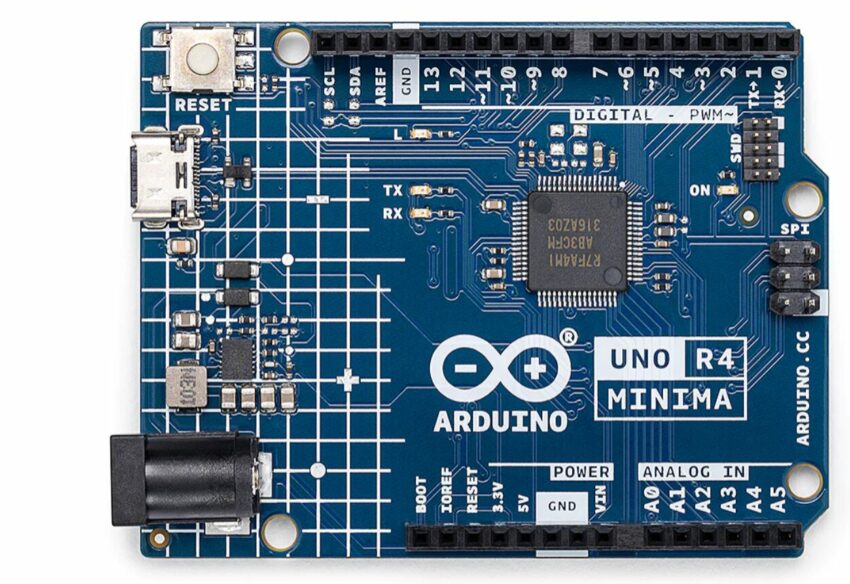
Arduino has collaborated with Renesas and Espressif to unveil the latest addition to its UNO family—the UNO R4. This new iteration boasts a remarkable 3x performance enhancement over the UNO R3 and is available in standard and Wi-Fi versions.
The UNO R4 is offered in two variants: UNO R4 Wi-Fi and UNO R4 Minima. It is equipped with the Renesas RA4M1 32-bit microcontroller, utilizing the Arm Cortex-M4 core to deliver a substantial increase in processing power, memory capacity, and overall functionality. In the Wi-Fi version, an Espressif S3 Wi-Fi module is integrated, opening up new possibilities for creative endeavors among makers, educators, and hobbyists.
Maintaining the beloved features of its predecessor, the UNO R4 prioritizes compatibility with the same form factor, shield compatibility, and 5V operating voltage. Additionally, software compatibility is a key focus, ensuring that most existing libraries and examples seamlessly function on the new board.
In essence, the UNO R4 represents a significant advancement in performance and functionality while preserving the familiarity and versatility that users appreciate in the UNO R3.
The UNO R4 Wi-Fi variant stands out by including Wi-Fi and Bluetooth Low Energy (BLE) connectivity, catering to users who seek versatile wireless capabilities. On the other hand, the UNO R4 Minima is designed as a budget-friendly option, providing the new microcontroller without additional features. Furthermore, Arduino IDE now supports other Renesas microcontrollers, like the RL78/G22 and G23, broadening the range of compatible devices.
Massimo Banzi, co-founder and chairman of Arduino, announced the UNO R4 during Arduino Day 2023. He believes the UNO R4 is a new chapter in the UNO story and the perfect way to move forward, leveraging the latest available technology. He said,
“While maintaining the UNO R3 in our product lineup, we collaborated closely with our partners Renesas and Espressif to create the most compatible and powerful maker board on the market. I’m eager to see the incredible projects the community will develop, particularly with the UNO R4 Wi-Fi. Imagine the possibilities for STEM educators and makers by utilizing existing shields and accessories and leveraging Wi-Fi to connect to the Arduino Cloud or other platforms.”
Renesas’ SVP, Chris Allexandre, said, “
We are honored to collaborate with Arduino on their iconic UNO product line. Despite the challenges of this intricate project with a rich legacy, our 5V 32-bit Arm Cortex M4-based microcontrollers facilitated a smooth upgrade path, offering enhanced performance and resources to unlock endless potential for makers worldwide. As both a technology company and an investor, we take immense pleasure in supporting Arduino’s mission to empower innovation by making advanced technology accessible and user-friendly for all.”
The Arduino UNO R4 introduces several notable improvements, featuring the Renesas RA4M1 microcontroller with an Arm Cortex-M4 core running at 48MHz. This enhancement results in a remarkable 3x performance increase compared to its predecessor, the UNO R3. To accommodate more complex projects, the SRAM has been upgraded from 2kB to 32kB, and flash memory has been expanded from 32kB to 256kB.
Recognizing the importance of software compatibility, extensive efforts have been made to ensure backward compatibility with existing code examples and tutorials for the UNO R4. Popular Arduino libraries are being optimized, aiming for seamless functionality in most cases. However, some libraries previously optimized for the AVR architecture in the UNO R3 may require porting to the new Renesas architecture. To support this transition, Arduino provides a public list of such libraries, along with links to alternative options. In a bid to encourage library developers to adapt their low-level code to the Renesas architecture, an early adopter program has been initiated, and interested developers can find more information on the dedicated website.
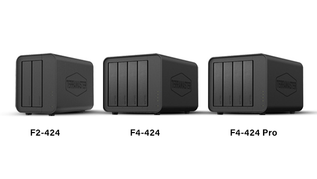
TerraMaster, a professional brand focused on providing innovative storage products for homes and businesses, recently introduced the 424 series, a new upgrade of 423 series. The brand-new 424 series adopts the Intel 12th Generation CPU Alder Lake N95, 8GB DDR5 memory, two 2.5GB network ports, two M.2 NVMe sockets, and adds a USB Type-C host interface and a USB Type A interface, achieving a 40% improvement in overall performance compared to the previous generation.
It’s worth mentioning that a more powerful version, the 424 Pro, has also been launched, equipped with an Intel Core i3 CPU and up to 32GB DDR5 memory, catering to the needs of individuals and business users who demand higher performance. The 424 series will come with the new generation TOS 5.1 operating system and can be smoothly upgraded to the TerraMaster TOS 6 operating system in the future.
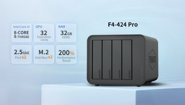
F4-424 Pro Key Features
Peak Performance 4-Bay NAS
Core i3 8-core 8-thread CPU at 3.8GHz (turbo), integrated UHD GPU at 1.25GHz, 32GB DDR5 4800MHz memory (non-ECC, non-upgradable), dual 2.5G Ethernet ports, and dual M.2 NVMe slots for SSD caching. An ideal peak performance NAS storage solution for small and medium-sized business users.
Faster Application Response
Equipped with a robust CPU and DDR5 memory, achieves a remarkable 150% performance boost over its predecessor. Experience 100% faster application load times, a 45% increase in file and photo retrieval speed, a 55% improvement in database response speed, and a outstanding 65% faster PHP response for web pages. Elevate your workflow efficiency with seamless high-load performance.
Higher Transmission Speed
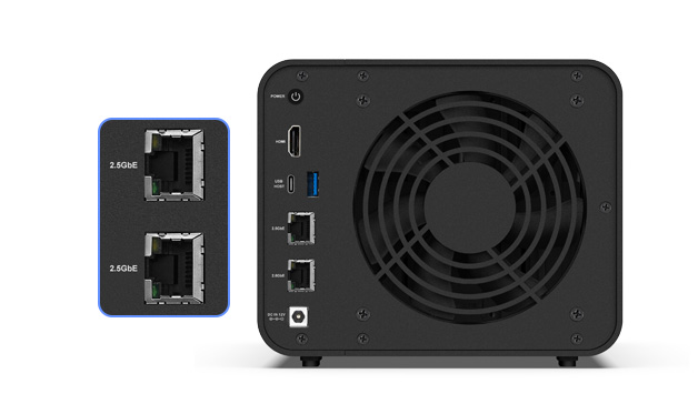
Features dual 2.5 GbE interfaces and can achieve a linear data transmission speed of 283 MB/s (tested with NAS dedicated HDDs 18TB x 4, RAID 0), Link Aggregation offers a network bandwidth up to 5 Gb, ideal for multi-user and high-concurrent file access. Featuring dual USB 3.2 Gen2 10Gbps interfaces, data transfer between your NAS and external devices is made swift.
Latest TOS System and Virtualized Applications
TNAS runs on TOS 5 and the coming TOS 6 system which integrates all-round professional storage management functions including network management, permission management, storage management, and resource monitoring via user-friendly, intuitive, and flat web interfaces.
The F4-424 Pro satisfies virtualized application needs and provides additional functionality within one device with the use of professional virtualized apps, including VirtualBox and Docker, and by cooperating with Docker-compose and Portainer. This lowers the cost of corporate investment in IT.
Rich Backup Solutions
Centralized Backup, Duple Backup, Snapshot, CloudSync, TFM Backup, and more enhance the security of your data with multiple backup applications. And the F4-424 Pro supports various RAID types, including RAID 0/1/5/6/10/JBOD/Single, and TRAID.
Easy M.2 SSD Installation
To facilitate the installation of M.2 SSDs, TerraMaster has specially designed a side sliding cover for the F4-424 Pro chassis, which is simply pushed aside to install M.2 SSDs. TerraMaster also provides hand-tightened screws, making it easy to install an SSD within 5 seconds.
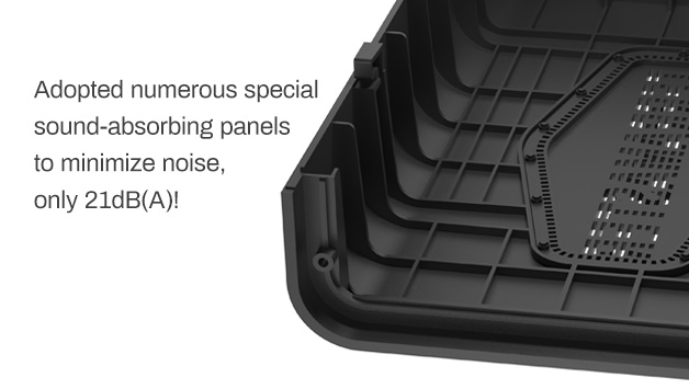
Less Noise
The F4-424 Pro adopts TerraMaster new structure which besides incorporating additional shock-absorbing measures, TerraMaster’s engineers have designed numerous special sound-absorbing panels in the new structure to minimize noise which is 50% lower than the previous generations, with a noise level in standby mode of only 21dB(A)!
In addition to the F4-424 Pro, the 424 series includes another 2 models: F2-424 (2-bay) and F4-424 (4-bay), catering to the demands of home users, SOHO, and small businesses for high-performance NAS.
The F4-424 Pro and F4-424 are already available in United States and select European markets, and will be generally available in other markets soon.