minUno development Board

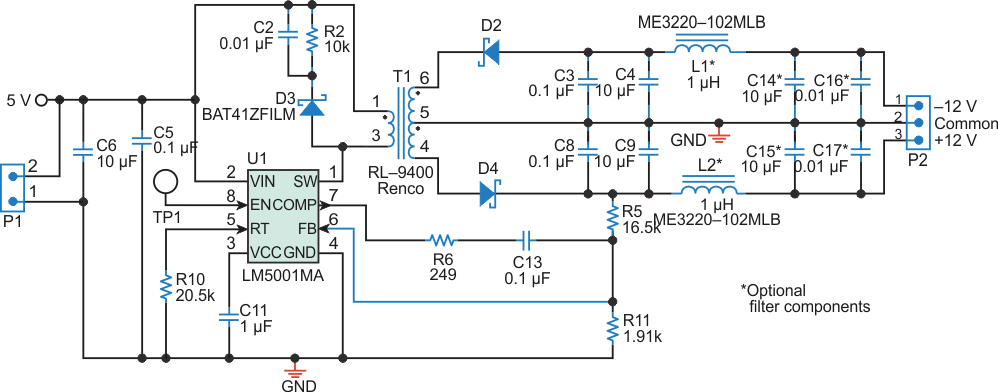
The Arduino Uno is unarguably one of the greatest development boards ever made and its impact as one of the boards that rekindled the fire of the electronics maker movement cannot be disputed. It came with enough power for users to build amazing projects, but it also was extremely easy to use making it a superb platform for learning electronics. However, there was one “shortcoming” users couldn’t ignore; the size of the Uno. While this was not a problem for professionals and semi-professionals who could easily migrate their project to an ATmega328p chip after prototyping with the Uno, it was a problem for beginners who would like to use the entire board in their project.  Several projects have made attempts at modifying the size, from projects like “barebone Arduino” to several “Arduino on Breadboard” projects but none of this projects has however been able to put together all the features of the Uno on a small form factor like Mellbell recently did with the minUno development Board. 

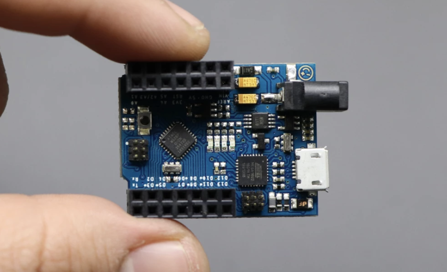
The miniUno is an exact replica of the Arduino Uno only that it is a quarter the size of the Uno, measuring only 1.35″ x 1.05″ compared to the 2.7″ x 2.1″ dimensions of the Arduino Uno. True to Mellbell’s claims about the board retaining the strength of the Arduino Uno, the miniUno is based on the Atmega328p (same microcontroller on the Arduino Uno), sports 14 digital I/O pins (6 of which can be used as PWM outputs), 6 analog input, a micro USB port, a power jack, and ready to go plug and play compatibility with the Arduino IDE.

The board was a follow up development to the Pico (“smallest Arduino Board”) which was launched by Mellbell a while back and retains the Popular MicroUSB ports (definitely one of the contributors to the reduced sized) which in conjunction with the pre-flashed bootloader on the board, allows seamless connection to the Arduino IDE, straight out of the box.

Some of the highlight features of the miniUno are listed below:

  • Size: 1.35″ x 1.05″
  • Weight: 5.5 grams
  • Digital I/O pins: 14 (of which 6 provide PWM output)
  • PWM Digital I/O Pins: 6
  • Analog Input Pins: 6
  • DC Current per I/O Pin: 20mA
  • DC Current for 3.3V Pin: 50mA
  • Microcontroller: ATmega328P
  • Operating Voltage: 5V
  • Input Voltage (recommended): 7-12V
  • Input Voltage (limit): 6-20V
  • Flash Memory: 32 KB (ATmega328P) of which 0.5 KB used by bootloader
  • SRAM: 2 KB (ATmega328P)
  • EEPROM: 1 KB (ATmega328P)
  • Clock Speed: 16 MHz
  • LED_BUILTIN: Yes (PIN 13)
The MiniUno

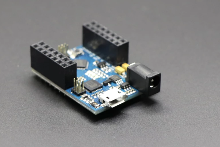
Standard pin headers were used on the miniUno making it easy to use with breadboards. The board’s performance has been likened to that of the Arduino Uno with the only thing missing being the huge size of the Uno

The MiniUno is currently available for sale on Mellbell’s website for $21 with a discount of up to $4 when you buy 20 of the boards. More information about the boards is available on the product page.

Perform Power Analysis Side-Channel Attacks with the ChipWhisperer-Nano

If you have ever considered the option of using encryption in your design, then you should be able to perform a side-channel attack as well as understand the consequences of such an attack on your product. While oscilloscopes and differential probes can be helpful in traditional power analysis attacks especially at the initial stage, these tools can be a bit of overkill for most analyses and also very expensive.

The ChipWhisperer series aims at nothing short of causing a fundamental change in the entire embedded security industry. A combination of documentation, training, open-source software and hardware makes it easy to master hardware security problems.

Whisperer Nano

The new ChipWhisperer-Nano from NewAE technology is a small form factor tool that contains a capture device as well as an STM32- based target both for side-channel attacks and for learning. Designed primarily for power analysis demonstrations and training programs, this latest release in the ChipWhisperer series is an ultra-low-cost platform for voltage fault injection and side-channel analysis.

Some of the features of the Chip Whisperer Nano include:

  • STM32F030 target for loading example code and a programmer built into the CWNANO.
  • Crowbar based VCC glitching with about 10nS resolution on the width of the glitch and glitch offset from the trigger with up to 200nS jitter.
  • ADC for sampling up to 20MS/s with either an internal clock (both synchronous and asynchronous) or an external clock (synchronous to the device).
  • ADC hardware trigger that uses rising-edge input and samples for user-configurable length.

The ChipWhisperer NANO’s capture hardware has a dedicated 8-bit ADC chip interfaced with a microcontroller which helps to sample the power rail and provide information back to the software. It then provides frequency and timing analysis of the power signal while the target runs its algorithms.

Example of Chipwhisperer Analyzer Software

Although the ChipWhisperer Nano lacks some other glitching features when compared with the other larger and more expensive tools in the SCA tool portfolio like the Pro and Lite, the ChipWhisperer Nano is an excellent learning tool with an estimated BOM cost of about $20 for a single unit.

The nature of the ChipWhisperer, being open source also makes it possible to engage the research community at large and at the same time, provides low-cost reference hardware. The Jupyter-based documentation provides examples like analysis for password bypass and AES attacks using different techniques.

To download the open-source software and various hardware options including the PDF schematic of the CWNANO, you can visit the ChipWhisperer GitHub repo or check ChipWhisperer-Nano website for information specific to the product.

New Surface-Mount Fully Integrated Current Sensors

The ACS772/3 family expands to include through-hole and surface-mount CB package options with enhanced working isolation voltage

Allegro MicroSystems, a global leader in power and sensing solutions for motion control and energy efficient systems, today announced significant ease-of-use enhancements to its popular high current fully integrated ACS772/3 current sensor “CB” package family.

These industry-leading, automotive grade high voltage isolation current sensors already provide economical and precise solutions for both AC and DC current sensing up to 400A. Building on that leadership and deep customer-understanding, Allegro’s new surface-mount leadform option for the CB package is the answer to many customer challenges by providing a flexible solution for space constrained applications.

“This is a classic, ‘You asked – we listened.’  innovation with purpose moment for us,” explains Shaun Milano, Business Unit Director for Current Sensors. “Our customers want flexibility, and we’re excited to provide these innovative, robust solutions in this new surface-mount option to complement our highly popular through-hole version. High current PCB designs improve power density and efficiency and this surface-mount option allows customers to realize these advantages with a simpler manufacturing process.”

The ACS772/3 family of current sensor ICs has an enhanced feature set that helps engineers simplify their bill of materials and improve efficiency in the toughest of applications:

  • Small form footprint over competing solutions
  • Very fast 2.5uS response time that enables overcurrent fault detection – ideal for safety-critical applications
  • Enhanced working isolation voltages up to 1300V+ for basic DC voltage, and 650V+ for reinforced isolation DC voltage – No need for opto-isolators or other costly isolation techniques.
  • High accuracy of +/-2.1% over the lifetime of the IC

These features make the ACS772/3 family ideal for a range of applications from industrial robotics to electric vehicles.

“Many of our customers, especially in green energy applications, are looking for higher working voltages which can provide efficiency improvements and cost reductions in their systems,” said Milano. “In solar applications for instance, raising the system voltage allows for longer strings, which eliminates significant wiring and connector combiner boxes.  It also allows for longer panel strings with higher rated output inverters, which reduces losses and improves efficiency.  These improvements are a win-win for our customers.”

For more details on the ACS772/3 family, including the new surface-mount option, and to learn more from Allegro’s current sensor team:

WIN SOURCE – A good place to buy cost-effective components online

There are thousands of different electronic component distributors  and suppliers around the world, who sell similar parts with a range of different prices. However, In the course of my internet search, i stumbled upon WIN SOURCE, a Hong Kong-based electronic component distributor of commonly-used components and obsolete parts since 1999. They boast of over hundreds of thousands of different electronic parts, with a pocket friendly price, especially if you are purchasing in bulk or individually.

They distribute and manufacture over 100 popular brands, over 500,000 SKUs stock. 365-day with 24 hours shipment is a bright spot. They also passed several authoritative quality certifications, including AS9120, ISO9001, ISO14001 at the same time.

Win-Source Electronics various Certifications

It is not only popular for their excellent services, certifications and website, they are also popular for the quality of their components as. Customer reviews shows that they have been satisfied with Win Source for its quality components and fast delivery. Any part you purchase has a one year warranty in case of anything is defective or wrong with them, coupled with their 24 hours delivery service, that making it one of the reasons why I would also recommend the company to all electronic enthusiast.

In order to purchase any component through their website, you have to create an account. It is a very simple process, they just need a few details. Creating an account enables you to receive personalized newsletters, and update you on everything which is going on.

WIN SOURCE’s website is very detailed and easy to navigate, with the catalog displaying the whole shop’s inventory, part-by-part, and also displaying the individual SKU, Ladder price and detailed description, etc.

It is worth mentioning that when I browsed the specification list, I found several special parameters, Fake Threat In the Open Market and Supply and Demand Status. This will be a valuable parameter for engineers in purchasing and purchasing. You can also check the ECAD Module and alternative parts recommendations.

They went a step further by operating a customer service email and a live chat service on their website, which is very convenient service for buyers. One aspect that is very user-friendly is that WIN SOURCE provides users with free electronic component campaign, which is really exciting for engineers who have difficulty selecting models or companies that produce sample tests.

They have various manufacturers under one site, so if for example I’m looking for integrated circuit products, when i search for it, it brings up various companies selling integrated circuits product page. This makes it easy for me to pick from a variety of products.

Another noteworthy service rendered by the company is their Return Policy which is reasonable, and also an Environmental, Anti-Counterfeit and Privacy Policy, to reassure you that they a trusted website to use. WIN SOURCE makes sure they maintain a high standard between them and their customers. Their payment methods include: VISA, Mastercard, American Express and PayPal, which are all secure and simple mediums for payment.

Search results on Integrated Circuits on Win-Source Electronics site

One interesting part of Win Source’s website, is the news section of it, there you can find the latest updates and news about what’s going on in the world of electronic components. News about the latest brands, updates about components and much more can be found on the news page on the website. They provide updates on the page regularly, so you can endeavor to visit the site every week.

In summary, I highly recommend Win Source Electronics products and services to all who are interested in purchasing products from them. They are a genuine and experienced company, they are capable of catering to the need of everyone, either those who are newbies in electronics, or people who are experienced in the electronics industry. You have a massive selection to choose from, this makes Win Source your go to for electronics. You can send an email to their support team, they are very friendly, and ready to answer all your questions, and provide you with the necessary information which you need. Visit Win Source Electronics’ website for more details and user experience.

MPPT charge controller reference design for 12- and 24-V solar panels

This reference design is a Maximum Power Point Tracking (MPPT) solar charge controller for 12-V and 24-V solar panels. This compact reference design targets small and medium power solar charger solutions and is capable of operating with 15- to 60-V solar panel modules, 12- or 24-V batteries and providing upwards of 20 A output current. The design uses a two-phase interleaved buck converter to step down the panel voltage to the battery voltage. The buck converter and its connected gate drivers are controlled by a microcontroller unit (MCU), which calculates the maximum power point using the perturb and observe method. The solar MPPT charge controller is created with real-world considerations, including reverse battery protection, software programmable alarms and indications, and surge and ESD protection.

Features

  • 96% efficiency in 12-V systems and 97% efficiency in 24-V systems
  • Wide input voltage range: 15 V to 60 V
  • High rated output current: 20A
  • Battery reverse polarity, over-charge and over-discharge protections
  • System over-temperature and ambient light detection capabilities
  • Small board form factor: 130 mm x 82 mm x 38 mm
TIDA-010042 MPPT charge controller reference design for 12- and 24-V solar panels block diagram image

more information: http://www.ti.com/tool/TIDA-010042

LaserPecker Pro – The Most Advanced Portable Engraver

LaserPecker Pro-The Most Advanced Portable Engraver. Compact, Safe & Easy-to-use ​Laser Engraver

LaserPecker recently announced a Pro version of their LaserPecker portable, affordable, compact laser engraver. Launched earlier this week on Kickstarter, the Laspecker Pro surpassed its modest funding goal of $10,000 in just 14 minutes and is currently approaching $200,000 with over three weeks left to go in the campaign. LaserPecker states their engraver can burn images, words, and patterns on nearly every material — food, metal, plastic, leather, and more.

According to the company,

“LaserPecker Pro is upgraded with an auto-adjusting support stand that sets up and focuses in seconds. All you have to do is put the engraving target on the spot. The built-in sensors of the stand will measure the distance between the laser generator and the target and automatically adjust the height to make sure the focal point is the correct distance from the surface of the object.”

LaserPecker upgraded the laser on the Pro version from a 450nm blue laser with 0.3mm light spot to a 450nm blue-violet laser with 0.15mm beam, which the company claims has over a 10,000-hour working lifespan. The Pro is a plug-and-play engraver ready to go outside the box and can use multiple power sources, including wall outlets, battery packs, and via USB Type-C cable.

Intro Video

As mentioned earlier, the LaserPecker Pro laser engraver is available now on Kickstarter with pledges starting at $269, which includes the engraver, safety goggles, materials package, magnetic protective shield, USB cable, and tripod stand. At the $369 level, you get the same goodies box, only it comes with the auto-focus support stand as well.

via www.hackster.io

simpleFE – A simple mixed signal front-end

simpleFE is a low cost, fully open-source, mixed-signal front-end. Designed primarily to carry out analog-to-digital and digital-to-analog conversion, simpleFE includes plenty of IO and allows you to create your own signal processing system more quickly, more easily, and more cost-effectively.

Features & Specifications

  • ADC: 8-bit, two channels, up to 7.5 Msps (I and Q)
  • DAC: 10-bit, two channels up to 7.5 Msps (I or Q) or 5 Msps (I and Q)
  • USB: High speed interface (USB 2.0)
  • GPIO: 16 pins
  • DAC Output: 10-bit, four pins
  • SPI: One interface
  • I²C: One interface
  • Antenna Connectors:
    • Two U.fl analog output (50 Ohm output impedance)
    • Two U.fl analog input (high impedance)

Components

  • USB: EZ-USB FX2LP (CY7c68013A)
  • FPGA: ICE40HX1K
  • Front-end: MAX5863
  • Software: GNURadio, gr-simplefe, libsimplefe C library

The project will launch soon on www.crowdsupply.com

DepthAI – An embedded platform for combining Depth and AI, built around Myriad X

DepthAI is a platform built around the Myriad X to combine depth perception, object detection (neural inference), and object tracking that gives you this power in a simple, easy-to-use Python API. It’s a one-stop shop for folks who want to combine and harness the power of AI, depth, and tracking. It does this by using the Myriad X in the way it was intended to be used – directly attached to cameras over MIPI – thereby unlocking power and capabilities that are otherwise inaccessible.

Real-time Object Localization

Object Detection is a marvel of Artificial Intelligence/Machine Learning. It allows a machine to know what an object is and where it is represented in an image (in ‘pixel space’).

Back in 2016, such a system was not very accurate and could only run at (rougly) one frame every six seconds. Fast forward to 2019, and you can run at real-time on an embedded platform – which is tremendous progress! But, what good does knowing where an object is in an image in pixels do for something trying to interact with the physical world?

That’s where object localization comes in. Object localization is the capability to know what an object is and where it is in the physical world. So, its x, y, z (cartesian) coordinates in meters.

This is what DepthAI allows. At 25 FPS.

The project is live on www.crowdsupply.com and has 28 days left.

High Power LED flashing beacon uses a switching regulator

This flasher/beacon circuit can be employed as a distress signal on highways, a direction pointer for parking lots, hospitals, and hotels, etc. The circuit uses a power LED, and provides more light than a typical incandescent lamp flasher. Use of a 6 V or 12 V SLA lantern battery makes the circuit portable.

The heart of the circuit is an MC34063 monolithic switching regulator subsystem, originally intended for use in DC-DC converters (Figure 1). This device contains a voltage reference, comparator, controlled duty cycle oscillator with an active peak current limit circuit, driver, and a high current output switch, all in an 8-pin DIP.

Figure 1. Functional Diagram of the MC34063.

The circuit briefly flashes a 1 W power LED from a 6 V to 12 V DC supply – at about 5% duty-cycle (Figure 2). Current limiting to the LED is accomplished by monitoring the voltage drop across R1, a 1 W sense resistor placed between VCC and the output switch, pin 1.

Figure 2. The Schematic Diagram of a Flashing Beacon.

The maximum current capability of a 1 W white LED is about 350 mA. At the beginning of a cycle, C1 starts to charge, and LED current rises rapidly, along with the drop across R1 which is monitored by the Ipk sense pin, IC1-7.

When this voltage becomes greater than 330 mV with respect to pin 6 (i.e., 330 mA), the current limit block in the IC provides additional current to charge the timing capacitor C1. This causes it to rapidly reach the upper oscillator threshold, at which point the output switch turns off and C1 discharges. Flashing rate can be altered by changing the value of C1. 100 µF gives approximately 4 Hz.

Since the LED flashes on very briefly, thermal issues are minimal and a star MCPCB is sufficient to cool the LED.

Create +/-12V Split Rail From A 5V Bias

With digital semiconductor technology driving system power supplies to lower voltages for higher performance and lower system power, sensitive analog sensor circuits face a growing problem. Much of the inherent noise created in the early stages of an analog sensor signal path is independent of the amplifier bias voltage, so using a higher bias voltage yields better accuracy and performance than a lower bias. With supply voltages dropping, then, designers must tolerate the loss of accuracy (SNR) due to the lower available voltage or derive a higher voltage bias from the available system supply.

In addition to the voltage, designers need to consider the ground. In many cases the sensor circuit must have bias voltages both above and below signal ground. That signal ground can be either a true system ground or a virtual ground created at the midpoint of a single-rail power supply. Using a true system ground requires “split-rail” biasing (±V), but yields improved performance as a result of reduced leakage currents and reduced variations in a virtual ground, both of which affect measurement accuracy.

Figure 1. A switch-mode regulator IC and transformer can create ±12-V bias voltages from a system’s 5-V rail
to help improve the performance and signal-to-noise ratio of analog sensor front ends.

To obtain the best performance from the analog front end, then, designers need a method of creating a higher voltage split-rail bias from a lower-voltage single-rail supply. One way to create this split-rail voltage is to use a switch-mode regulator IC in concert with a small transformer. This forms a flyback design that uses less than one square inch of board space.

The circuit of Figure 1 boosts a nominal 5-V single-rail supply (4.5 to 5.5 V) to a low-noise, ±12-V bias and can be adapted to develop other voltages such as ±15 V. The design uses a Texas Instruments LM5001 (U1) switch-mode regulator that integrates a pulse-width modulation (PWM) generator, a switching transistor, a voltage reference, and an error amplifier that controls the PWM duty cycle based on a comparison between the reference and the feedback signal on pin 6.

The regulator switches current through the primary of center-tapped transformer T1, and the PWM duty cycle determines the output voltage at the secondary. Diode D3 and its attached components serve as a snubber to minimize transient noise and ringing on the transformer input when the regulator’s internal switch opens. Diodes D2 and D4 serve as half-wave rectifiers for the transformer’s output.

Figure 2. C biasing dominates losses in the split-rail bias circuit at lower currents,
but conversion efficiencies greater than 80% are attainable.

Resistor R10 sets the PWM’s nominal switching frequency to 600 kHz, which represents a compromise between conversion efficiency and noise (both switching noise and ripple) on the bias voltage outputs and transformer size. With this frequency, conversion efficiency (Fig. 2) can be greater than 80% depending on load. Both noise and conversion efficiency decrease with increasing switching frequency, so designers can choose to increase efficiency at the expense of noise by adjusting the value of R10. Decreasing the switching frequency often results in the need to increase the size of the transformer, adding to this tradeoff decision.

Capacitors C3, C4, C8, and C9 serve as the principal output filters, but designers can further reduce switching noise by incorporating the optional low-pass post filters L1/C14 and L2/C15 shown on the positive and negative outputs. The filters have a cutoff frequency of about 90 kHz, resulting in less than 10-mV peak-to-peak transient noise and under 2-mV switching ripple measured from dc to 600 MHz. Designers can reduce this noise even further by changing C4 and C9 to 47 µF. Symmetrical layout of the design’s differential power section can help reduce differential noise.

This type of flyback design, which uses only one regulator monitoring the positive output, provides common-mode rejection of some noise components and only uses a single IC. Cross regulation is typically not as tight with one regulator as would be possible when using a separate regulator for the negative output. But since most sensor signal path circuits draw symmetrical current on each rail, cross regulation usually isn’t an issue.

In any case, measurements show good cross regulation with this circuit. Either output maintains regulation to less than 3% when delivering 35 mA while the other output load varies between 10 mA and 50 mA. The design’s measured output tolerance is within 5 mV across both outputs when delivering from 5 to 40 mA from both outputs differentially.


TOP PCB Companies