New Broadband Hybrid Silicon-InGaAs Photodetectors

Marktech Optoelectronics, Inc. (Marktech), a privately-held, VOSB-certified, leading designer and manufacturer of standard and custom optoelectronics components and assemblies, including ultraviolet (UV), visible (VIS), near-infrared (NIR), and short-wave infrared (SWIR) emitters, detectors, InP epiwafers and other materials, today announced the global market introduction of its Models MT03-041 (TO-5) and MT03-047 (SMD), two new broadband hybrid Silicon-InGaAs photodetectors.

The industry-exclusive design of the Models MT03-041 and MT03-047 ensures versatile, accurate, reliable broadband detection over spectral ranges from UV-to-VIS-to-SWIR, with 250 nm (UV) to 1750 nm (SWIR) enhanced sensitivity. This wide dynamic range includes 365 nm blue-green enhanced Silicon-based and 1300 nm InGaAs-based detection, respectively; ultra-low-noise measurement performance; and high shunt resistance. The detectors are seamlessly integrated within a single, compact thru-hole or SMD package. They are also both REACH and RoHS compliant.

Small-to-medium-sized quantities of standard Models MT03-041 (TO-5) and MT03-047 (SMD) are typically available with 24-hour shipment from stock via Marktech global distribution partner, Digi-Key Electronics. Optional accessories for Models MT03-041 (TO-5) and MT03-047 (SMD), also available from Marktech, include UV-to-IR-to-SWIR range emitters. Each emitter may be mechanically and spectrally matched, then combined with the photodetector as a single, compact package. Custom designs may be produced in as few as 6-8 weeks from customer prototype approvals. Please consult Marktech’s Latham, New York global corporate headquarters and R&D center for assistance.

Typical applications for Marktech broadband hybrid Silicon-InGaAs photodetectors include medical, industrial, high-speed communications, security and spectroscopy. For more information about Models MT03-041 (TO-5) and MT03-047 (SMD), or other products and services available from Marktech, visit www.marktechopto.com.

1.14″ 240×135 Color TFT Display + MicroSD Card Breakout – ST7789

Say hello to the 1.14″ 240×135 Color TFT Display w/ MicroSD Card Breakout. It’s the size of your thumbnail, with glorious 240×135 high res pixel colour. This very very small display is only 1.14″ diagonal, packed with RGB pixels, for making very small high-density displays.

It’s so small only 1.14″ diagonal but has a high density of 260 PPI, 240×135 pixel display with full-angle viewing. It looks a lot like the 0.96″ 160×80 display but has 2.5x as many pixels. We’ve seen displays of this calibre used in smartwatches and small electronic devices but they’ve always been MIPI interface. Finally, here is one that is SPI and has a friendly display driver, so it works with any and all microcontrollers or microcomputers!

This lovely little display breakout is the best way to add a small, colourful and very bright display to any project. Since the display uses 4-wire SPI to communicate and has its own pixel-addressable frame buffer, it can be used with every kind of microcontroller. Even a very small one with low memory and few pins available! The 1.14″ display has 240×135 16-bit full-colour pixels and is an IPS display, so the colour looks great up to 80 degrees off-axis in any direction. The TFT driver (ST7789) is very similar to the popular ST7735, and the Arduino library supports it well.

The breakout has the TFT display soldered on (it uses a delicate flex-circuit connector) as well as an ultra-low-dropout 3.3V regulator and a 3/5V level shifter so you can use it with 3.3V or 5V power and logic. They also had a little space so they placed a microSD card holder so you can easily load full-colour bitmaps from a FAT16/FAT32 formatted microSD card.

Of course, we wouldn’t just leave you with a datasheet and a “good luck!” – we’ve written a full open source graphics library that can draw pixels, lines, rectangles, circles, text and bitmaps as well as example code and a wiring tutorial. The code is written for Arduino IDE but can be easily ported to your favorite microcontroller!

The module is on sale at adafruit.com for $9.99

Current Limit Solid State Power Switch with Latch

The project published here is a solid state power switch with current limiting that prevents damage to host devices from faulty load conditions. This analog current limit switch have low on-resistance P-channel MOSFET and INA202 driver IC from Texas instrument. The project operate from input voltage in the range 5V to 24V and can handle current up to 2Amps .The versatile project can be used in Smart Power applications. It is widely used to clamp the overload current, deliver constant current.

The project provides 2A current, if load current increases more than set point (2amps) automatically isolates the switch. The over-current limit threshold is set to 2 Amps but it can be programmed using an external resistor R7 and PR1 and by changing value of Shunt resistor R1, refer data sheet of INA202 for more information for current adjustment and current limit. Circuit also requires 5V logic supply other than the load supply. Trimmer potentiometer helps to set the threshold current. Setting the output is simple using trimmer pot, turn the trimmer potentiometer counter clockwise and connect current meter between load , tie the reset wire to VCC 5V switch on the logic supply and logic supply, turn the pot till it is  latches the output. D1 is power LED.

Current Limit Solid State Power Switch with Latch – [Link]

The Top 10 Operational Amplifiers on SnapEDA

The operational amplifier – or “op amp” for short – is a common building block in analog electronics. Whether you’re a professional electronics designer or just getting started, it is likely you’ve used an op amp in your designs.

Invented in 1941 by Karl D. Swartzel Jr. of Bell Labs, the op amp was originally built with vacuum tubes and was invented to perform mathematical operations in analog computers, hence how it earned its name. Now, op amps are used in all kinds of applications, for everything from signal conditioning, filtering, as well as for complex mathematical operations such as integration and differentiation. They form the basis of many modern analog electronic circuits because they are cost-effective, perform optimally and are readily available.

Op amps are commonly available as integrated circuits (ICs). They have input and output terminals capable of giving out a larger version of voltage signals that are being passed through them. They can be designed to act as a voltage amplifying device when used with active components such as transistors and passive components like resistors and capacitors to provide the desired response.

When signals pass through discrete elements in an analog circuit, they tend to decrease in amplitude—their voltage level decreases, but an op amp can help buffer and boost the amplitude of such signals, hence, delivering a signal that is useful at the output.

Op amps are very adaptable and versatile to many electronic circuits. They are used in audio and video applications, voltage regulators, precision circuits, analog-to-digital and digital-to-analog converters, and many other applications.

#10 LM741H from Texas Instruments

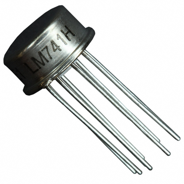
The LM741H is a general-purpose operational amplifier that comes in an 8-pin TO-99 package with a nominal supply voltage range of ±15V. It has a large signal voltage gain of 200V/mV and bandwidth of up to 1.5MHz. Its input and output come with overload protection. This op amp also features no latch-up when the common-mode range is exceeded. It is a direct, plug-in replacement for other op amps like the 709C, LM201, MC1439, and 748 in most applications.

Average price across distributors at time of publish: $11.78

#9 LM324AMX/NOPB from Texas Instruments

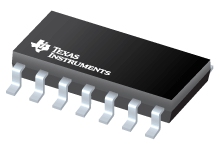
The LM324AMX/NOPB comes with four internally compensated op amps all in a 14-pin SOIC package. It is a low power general-purpose operational amplifier that features a large signal voltage gain of about 100 V/mV, a wide gain-bandwidth of 1MHz and a low input bias current of 45 nA. It operates from a single power supply over a wide range of 3 V to 32 V and also supports dual supplies with a range of ±1.5 V to ±16 V. It is suitable for transducer amplifiers, DC gain blocks, conventional op amp applications.

Average price across distributors at time of publish: $0.29

#8 MCP6001T-I/OT from Microchip

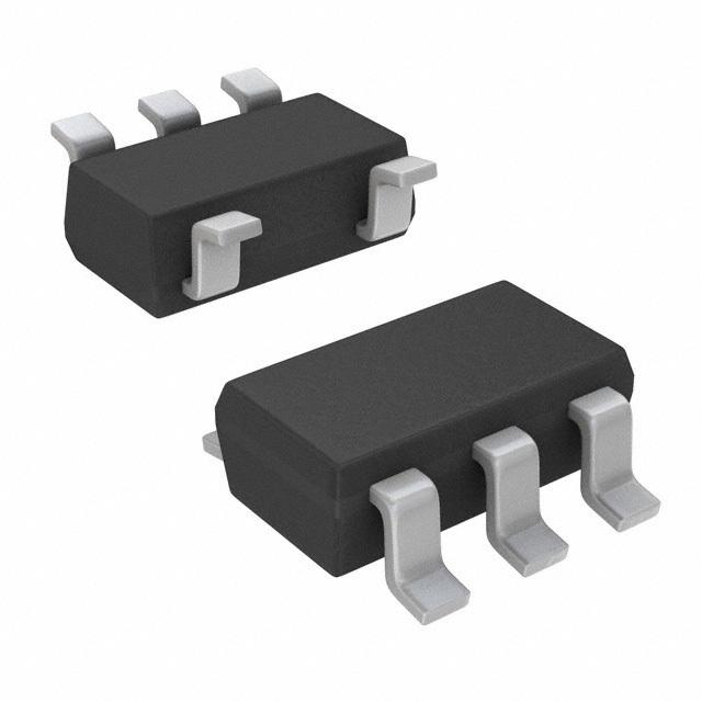
The MCP6001T-1/OT is a single general-purpose op amp that comes in a 5-lead SOT-23 package and an industrial temperature range of -40°C to +85°C specifically designed for low-cost and low-power applications. It operates with a single supply voltage going as low as 1.8V while drawing 100 µA (typical) quiescent current, and as high as 6.0V. It has a typical gain-bandwidth product of 1 MHz. Its features make it suited for battery-powered applications, automotive applications, portable equipment, and analog filters.

Average price across distributors at time of publish: $0.24

#7 LM324N from Texas Instruments

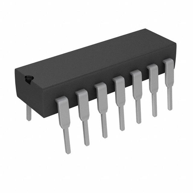
The LM324N is a low power quad operational amplifier that comes in a 14-pin DIP package with similar features to the LM324AMX/NOPB except with a wide gain bandwidth of 1.3MHz, a low input bias current of 20nA with a maximum input offset voltage of 5 mV.

Average price across distributors at time of publish: $0.52

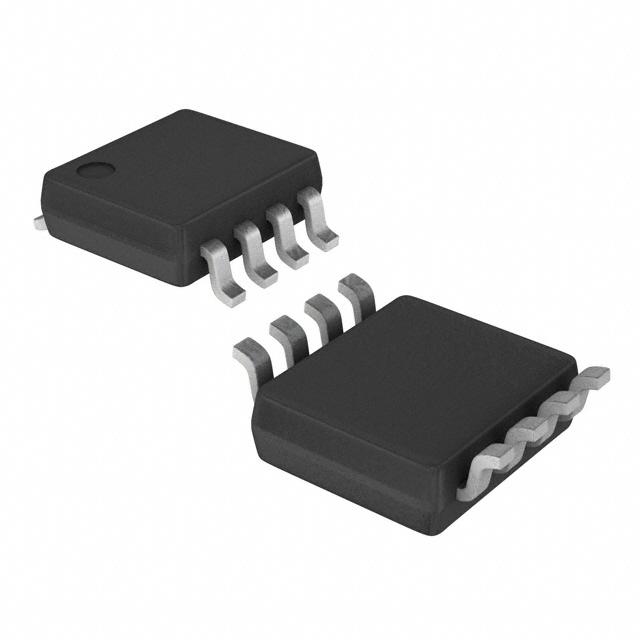
#6 LM358DT from STMicroelectronics

The LM358DT comes with two independent, high gain, internally frequency-compensated op amps packaged in an 8-pin SOIC package with an operating free-air temperature range of 0 °C to 70 °C. It operates from a single power supply with a range of 3 V to 32 V and also supports dual supplies with a range of ±16 V. It has a large signal voltage gain of 100V/mV and a wide gain-bandwidth of 1.1MHz. It has a typical input offset voltage and current of 2mV and 2nA respectively. Suitable for all conventional op amp circuits.

Average price across distributors at time of publish: $0.48

#5 UA741CP from Texas Instruments

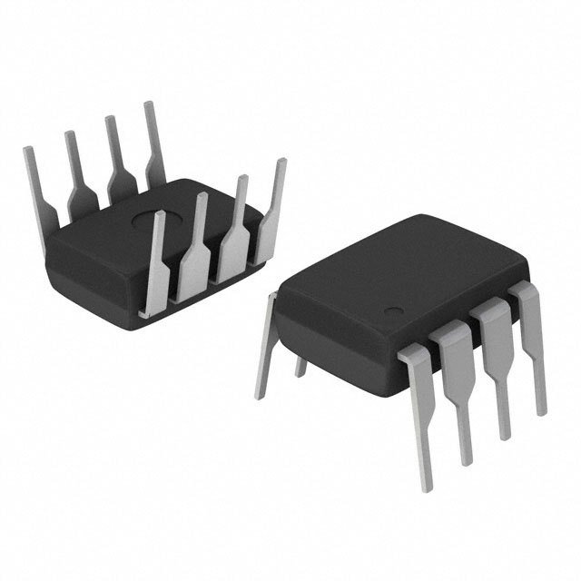
The uA741CP is a general-purpose operational amplifier that comes in an 8-Pin PDIP Tube featuring short-circuit protection, offset-voltage null capability. It has a nominal supply voltage range of ±15V, a large-signal differential voltage gain of 200V/mV. Its internal frequency compensation ensures its stability without external components. A low-value potentiometer may be connected between the offset null inputs to null out its offset voltage. Its high common-mode input voltage range and the absence of latch-up makes the amplifier ideal for voltage-follower applications.

Average price across distributors at time of publish: $0.48

#4 LM358N from ON Semiconductor

The LM358N is a dual-input operational amplifier similar to #6 – LM358DT – except that it comes in an 8-pin DIP package, has a typical input offset voltage and current of 2.9mV and 5nA respectively and has a typical and maximum input bias current of 45nA and 250nA respectively.

Average price across distributors at time of publish: $0.77

#3 LM358AN from ON Semiconductor

The LM358AN is a single supply dual operational amplifier, the same as #4 – LM358N – except with a maximum input offset voltage and current of 3mV and 30nA, and a typical and maximum input bias current of 45nA and 100nA, all lower than the LM358N.

Average price across distributors at time of publish: $0.58

#2 LMV358IDGKR from Texas Instruments

The LMV358IDGKR is a dual low-voltage rail-to-rail output op amp that comes encased in a VSSOP-8 package type with 1-MHz unity-gain bandwidth. It typically operates between 2.7 V to 5.5 V with a supply current of 210 μA. The LMV358IDGKR is a cost-effective solution for applications where low-voltage operation, space-saving, and low cost are needed.

Average price across distributors at time of publish: $0.62

#1 LM358ADT from STMicroelectronics

The LM358ADT is the same as #6 – LM358DT – except for the typical input offset voltage current of 1mV and a maximum input offset current of 10nA. It also has a maximum input bias current of 50nA which is lower than the LM358DT.

Average price across distributors at time of publish: $0.42

by Henry Egejuru @ SnapEDA

Eclypse Z7: Zynq-7000 SoC Development Board with SYZYGY-compatible Expansion

The Eclypse Z7 is Digilent’s newest FPGA/SoC designed to enable systems that are ultra high-speed and highly modular, featuring Xilinx’s Zynq-7000 PSoC. Zynq, plus the Zmod expansions and Digilent’s new software architecture results in a powerful research and prototyping platform optimized for productivity and accelerated design flow, making it the perfect product for instrumentation applications such as software defined radio, ultrasound, medical technology, and much more. As a host board for Zmods, the open-source SYZYGY-compliant expansion modules, Eclypse Z7 is designed to be highly flexible without the overhead of starting designs from scratch. Check out our Zmod ADC 1410 and Zmod DAC 1411 for more information!

Users can get started with the Eclypse Z7 immediately as Petalinux is supported right out of the box. Pre-built Linux images are accompanied by a software API for bulk data transfer. Digilent offers fully open and customizable hardware designs, Linux images, and Linux software applications.

Features:

  • Zynq 7020 SoC
    • 667 MHz dual core ARM Cortex-A9 processor
    • 13,300 logic slices
  • 1GB DDR3L with 32-bit bus @ 1866 MHz
  • 2x SYZYGY standard interface connectors for Zmod expansion
    • Standard supports data rates of up to 500 MHz
  • 2x Pmod connectors for Pmod expansion
  • Micro USB port for USBUART and JTAG programming
  • JTAG programming header
  • Programming mode select jumper: JTAG, QSPI, SD
  • Ethernet connector with 10/100/1000 Ethernet PHY
    • MAC address loaded into QSPI flash during manufacturing
  • Micro USB connector for user USB Host/Device/OTG
  • MicroSD card slot
  • Power jack
    • 12V, up to 5A
  • 2x user RGB LEDs
  • 125 MHz oscillator connected to Zynq PL for PL-only designs
  • 2x user buttons

more information: https://store.digilentinc.com/eclypse-z7-zynq-7000-soc-development-board-with-syzygy-compatible-expansion/

SMARC 2.0 CPU Modules based on NXP i.MX8M Processors

IBASE Technology Inc. (TPEx: 8050), a global provider of industrial motherboards and embedded computing solutions, announces the RM-N8M Series SMARC 2.0 Computer-on-Modules using 64-bit NXP i.MX8M application processors with ARM technologies for industrial and transportation computing solutions. The RM-N8M Series scalable platforms power various embedded systems with flexible and expandable features for smart factory, imaging, machine vision, gateway, in-flight entertainment and rolling stock applications including passenger information, entertainment and communications systems.

“We are pleased to leverage the scalability of the i.MX 8 series of applications processors to reduce time-to-market for our customers,” said Archer Chien, Director of Solution Product Planning Dept. at IBASE. “The RM-N8M takes advantage of these performance-scalable multicore platforms to enable highly integrated control systems with advanced graphics, imaging and computational capabilities.”

The new RM-N8M SMARC Series targets lower power and small form factor systems, and measures only 82mm by 50mm. It features high flexibility in terms of platform design and customization for end-user applications, while reducing development time and accelerating time to market. Equipped with 3GB soldered LPDDR4 and up to 64GB eMMC Flash memory, it has an extensive set of I/O support with 1x GbE, 2x USB 3.0/2.0, 2x MIPI CSI-2 video inputs, 2x PCI-E (x1) Gen2, 2x SPI/eSPI, 4x UART, 4x I2C, 2x I2S, and 12x GPIO. Display connections are provided by a 1080p MIPI Display Serial Interface (DSI) and HDMI V2.0a with up to 4K resolution.

The ARM Cortex-A53 based RM-N8M modules ship with 15-year longevity support and have been pre-qualified with Yocto v2.5 and Android 9 operating systems. The commercial grade variant supports dual-/quad-core 1.5GHz processors and 0°C to +70°C operating temperature range while industrial grade counterparts run with dual-/quad-core 1.3GHz CPUs and at -40°C to +85°C extended temperature. Also available is the RP-103-SMC, a 3.5-inch disk-size evaluation carrier board providing a broad range of interface and a 12V~24VDC input.

RM-N8M

RM-N8M Series FEATURES:

  • With NXP Cortex-A53/Cortex-M4, i.MX 8M Dual/Quad 1.5GHz processor
  • 3GB LPDDR4, 8/16/32/64GB eMMC
  • Rich peripheral I/O support
  • Validated with Yocto v2.5 and Android 9
  • Long life time supply with NXP solution
  • Compliant with SGeT standard SMARC™ V2.0

No pricing or availability information was provided for the RM-N8M, but it will likely ship before the “preliminary,” i.MX8M Mini based RM-N8MMI module and RP-103-SMC carrier board. More information may be found in Ibase’s RM-N8M announcement and its product pages for the RM-N8M, RM-N8MMI, and RP-103-SMC.

Current Limit Solid State Power Switch with Latch

The project published here is a solid-state power switch with current limiting that prevents damage to host devices from faulty load conditions. This analog current limit switch has low on-resistance P-channel MOSFET and INA202 driver IC from Texas Instrument. The project operates from input voltage in the range of 5V to 24V and can handle currents up to 2A. The versatile project can be used in Smart Power applications. It is widely used to clamp the overload current and deliver a constant current.

The project provides a 2A current if the load current increases more than the set point (2amps) automatically isolates the switch. The over-current limit threshold is set to 2 Amps but it can be programmed using an external resistor R7 and PR1 and by changing the value of Shunt resistor R1, refer datasheet of INA202 for more information on current adjustment and current limit. The circuit also requires a 5V logic supply other than the load supply. The Trimmer potentiometer helps to set the threshold current. Setting the output is simple using a trimmer pot, turning the trimmer potentiometer counterclockwise and connecting the current meter between loads, tying the reset wire to VCC 5V switch on the logic supply and logic supply, and turning the pot till it latches the output. D1 is the power LED.

Features

  • Supply Load 5 to 12V ( 24V Possible by Changing R6)
  • Supply Logic 5V DC
  • Maximum Load 2Amps
  • PR1 Trimmer Potentiometer Threshold Adjust
  • PCB Dimensions 44.33mm X 16.78mm

Schematic

Parts List

Connections

Photos

Video

INA202 Datasheet

Qualcomm SDA845 SoC-Based Module Targets Drone Designs

Intrinsyc Technologies announced the Open-Q 845 µSOM (micro System on Module) and Development Kit, to be available in the fourth quarter of 2019. The Open-Q 845 µSOM is the latest product in the evolution of Intrinsyc’s µSOM computing module series. It is an ultra-compact (50 mm x 25 mm), production-ready embedded module, well suited for powering the most advanced robotics, drones, cameras and embedded IoT devices requiring the latest on-device AI powers. Featuring the Qualcomm SDA845 system on chip (SoC) from Qualcomm Technologies, the 845 µSOM integrates many new features and capabilities in the same small form-factor:

  • Higher performing Octa-core CPU – up to 2.6 GHz on Gold cores
  • New hardware-based security layers for vault-like defense
  • Third generation Qualcomm AI platform for immersive, on-device intelligence
  • Four camera ports with flexible configurations supports up to 7 cameras
  • New camera architecture for cinema grade video capture
  • DisplayPort 4K60 via USB Type-C with USB super-speed data concurrency
  • Additional USB3.1 port for device connectivity while using DisplayPort
  • Gen3 PCIe interface.

This new hardware platform will be supported by your choice of full-featured Android 9 or Yocto Linux operating systems, with plans for offering Android 10 by Q2 next year. The Android 9 operating system will be shipped on the development kit and is a starting point for evaluation of the SOM and to kick-start your product development. If you prefer a Linux OS, that will be available to download from Intrinsyc and program onto your development kit. Full software documentation will also be included with purchase of the development kit.

more: www.intrinsyc.com

Otii by Qoitech helps developers achieve long battery life of their products

Low energy consumption is one of the major triggers of scalable product launch and maintenance. When your product is power-hungry, you are bound to receive negative reviews from your customers or get your app deleted altogether. So every developer wants to achieve long battery life of their products; developers are increasingly looking for ways to address the challenges of power consumption.

The award winning Otii by Qoitech attempts to address this problem by making energy optimization become more accessible.  Designed to empower developers to work better and smarter, Otii gives a full grasp into what causes battery drain throughout a product cycle and how likely pitfalls can be avoided. With this tool, you can measure and analyze battery power, that way you can reduce energy consumption by automating common repetitive tasks.

The Otii comes in two variants; the Otii Standard and the Otii Enterprise. Here is a comparison between the two to help you choose the right option for your needs.


However, the Otii Enterprise is best for individuals keen on having an even more efficient product development and testing. Its special set of features make it great for continuous integration, test automation and many more use cases. The Otii enterprise has everything in the Otii standard with some extra enterprising features like built-in scripting which can be used to automate repetitive tasks, TCP-server to help you control your Otii from any system that supports communication over TCP sockets, battery profiling to help find the best fit among various battery options and battery emulation used during device development to test its behavior when it is running out of power.The Otii standard is the tool for designing high energy efficient devices. It comprises of the Otii arc and the Otii software. The arc acts as a current and voltage measurement unit as well as a power supply to the device being tested while the software is a desktop application that is easy to use in Windows, Mac and Ubuntu Operating System.

Meanwhile, the battery toolbox is one important part of this tool that makes it worth considering. With the battery toolbox, users can be guided to pick the right battery for their device and application. The toolbox has features that profile real batteries for IoT and gives practical insight about the battery that is the best fit for your product. During its early stage of development, the toolbox sets the overall energy consumption expectations and later verifies that the initial assumptions about the battery product’s battery life did not change during its iterative process. The battery toolbox comes with a software license which when purchased and activated, is assigned with the Otii app.

Some specific features of this toolbox include:

  • Intuitive and easy-to-use UI for battery profiling
  • Create, edit and share battery models
  • Emulate battery’s output during discharge cycle at different levels of used capacity.
  • Set conditions for current-load, discharge level and time
  • Check when the cut-off voltage of the device under test is achieved
  • Emulate serial and parallel battery setups and,
  • Library selection of battery discharge profiles.

It’s high time you stop your device from being a serious battery drain. This all-in-one developer asset is a flexible tool every developer should have. The Otii is an affordable solution and it is sold through authorized distributors.

more information: https://www.qoitech.com/products/enterprise

Display Adapter For HDMI To Type-C With DP And PD Function

Main features

  • Operating Voltage: 5V
  • Output Voltage: 3.3V
  • Power Supply: USB Type-A to DC 5.5mm
  • Main Chip: lontium LT6711A
  • This adapter is designed for: DM-DevKit-AR0701
  • This adapter can be used with HDMI interface computers, ipads, game consoles and other devices.

The adapter is on sale for $79.99 on www.displaymodule.com

TOP PCB Companies