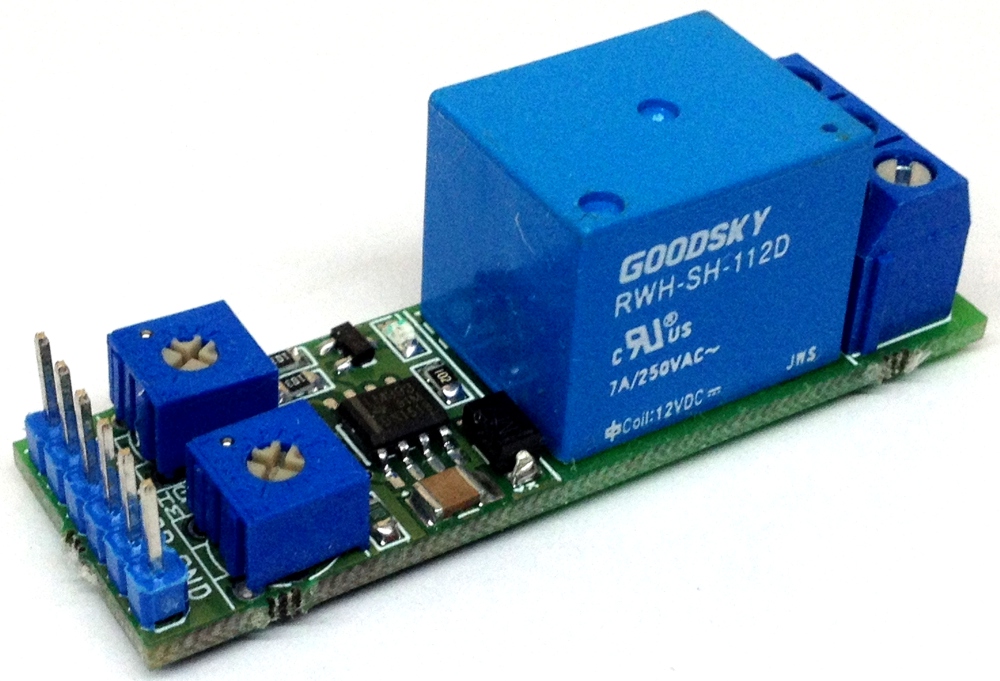
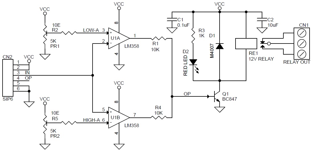
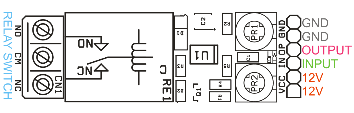
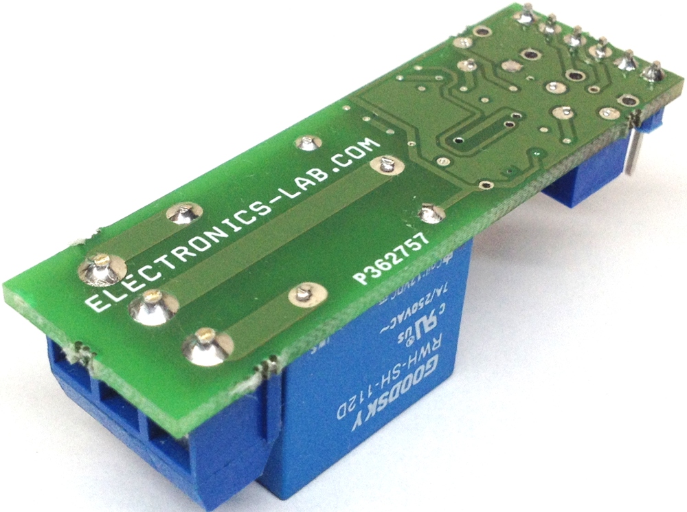
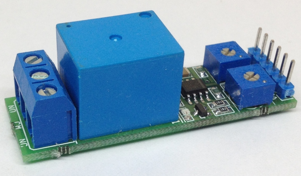
A window detector circuit, also called window comparator circuit or dual edge limit detector circuit is used to determine whether an unknown input is between two precise reference threshold voltages. It employs two comparators to detect over-voltage or under-voltage condition.
This circuit utilizes two comparators in parallel to determine if a signal is between two reference voltages. If the signal is within the window, the output is low thus RELAY is in off condition and also LED is off. Relay provides normally ON and normally OFF switch. If the signal level is outside of the window, the output is high and Relay is in ON condition. For this design, the reference voltages are generated with help of two Trimmer potentiometer. One pot used to set the high voltage level and another one to set the low level voltage adjust. LM358 op-amp used as comparator, it circuit works with 12V DC supply and consumes 50mA current when Relay is in ON state.
Window Comparator – Window Detector with relay output – [Link]
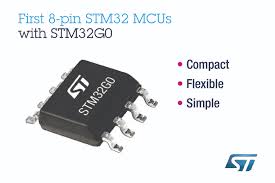
STMicroelectronics has launched a series of STM32 MCUs in an 8-pin package to provide simple embedded projects with 32-bit performance and flexibility in a small, cheap form factor. via www.eenewsembedded.com
The four new STM32G0 devices have a combination of 8-pin economy and a 64MHz Arm Cortex-M0+ CPU providing 59 DMIPS, up to 8Kbyte RAM and 32Kbyte flash on-chip. |The devices also have high-performing peripherals including a 2.5Msps ADC, high-resolution timer, and a high-speed SPI. The internal oscillator is accurate to ±1% over wide temperature and voltage ranges to save external clock components.
Utilising the low-power design features of the STM32 MCU range, the 8-pin STM32G0 devices can be used in energy-conscious applications governed by battery-capacity limits or eco-design legislation.
The new MCUs also provide scalability through the features available across the STM32G0 series, which offers up to 100 package pins, up to 512Kbytes Flash, additional high-performance analogue peripherals, and cyber-protection features.
STM32G0 MCUs are available now in 6mm x 4.9mm SO8N. The 8-pin Discovery kit STM32G0316-DISCO provides quick and affordable evaluation. STM32G031J6, STM32G031J4, and STM32G041J6 Access Line MCUs are also available in SO8N, offering additional functionality including a hardware AES acceleration, Securable Memory Area enabling secure boot or firmware update, extra timers, and 96-bit unique device ID.
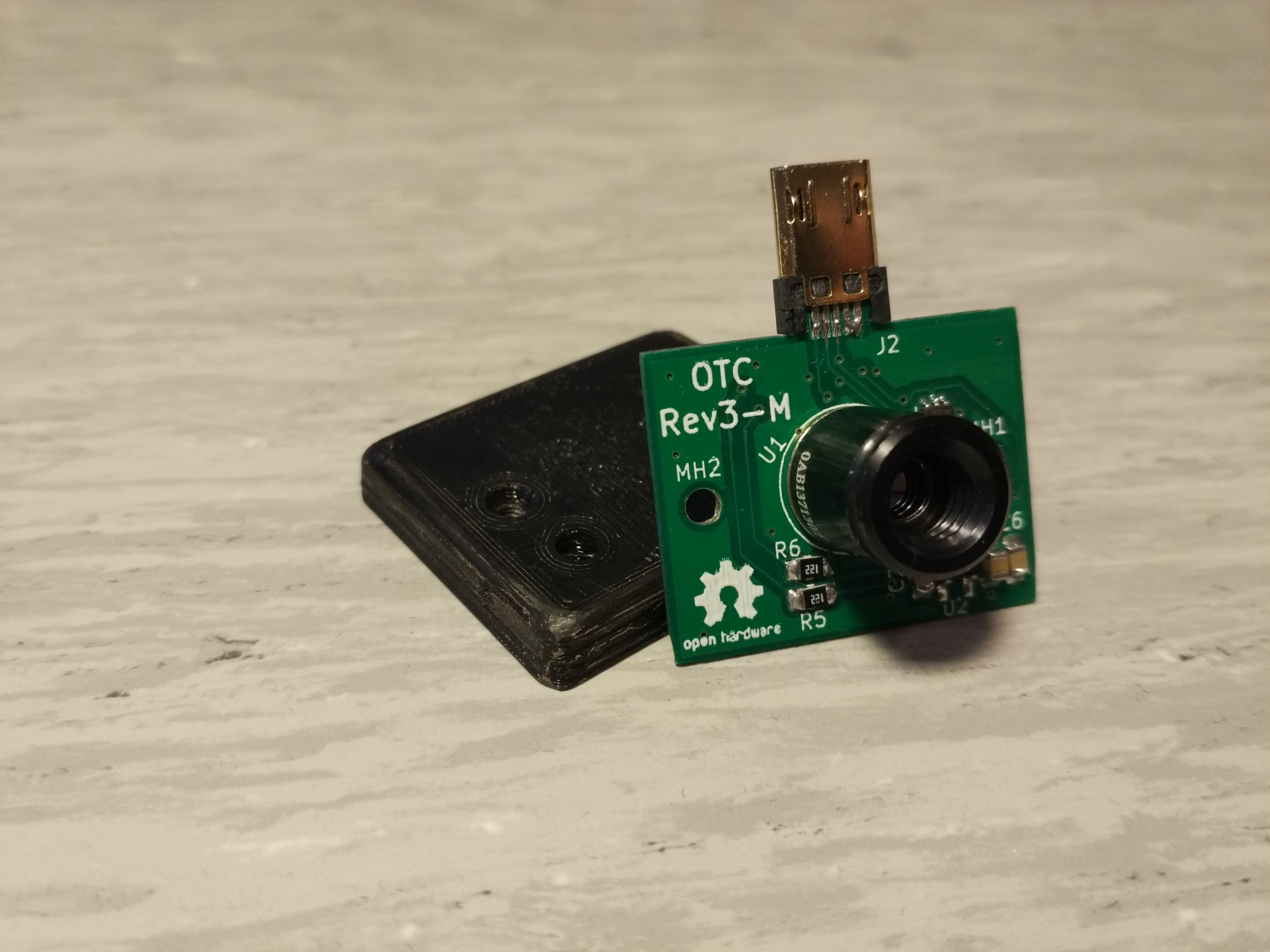
One application of thermal imaging which has been experiencing a surge in recent times is the application of thermal imaging in the detection of faults in circuits. While this has proven a very interesting and reliable way for evaluating Circuit boards before committing to mass production, the cost of the standalone solutions and even the smartphone adapter based thermal cameras and accompanying app has been a challenge for most users as they are usually expensive and not open source. To solve this problem and democratize access to the thermal camera for use in Circuit evaluation, TheMarpe, has developed an Open-source alternative which is rightly called the Open Thermal Camera.
The Open Thermal Camera
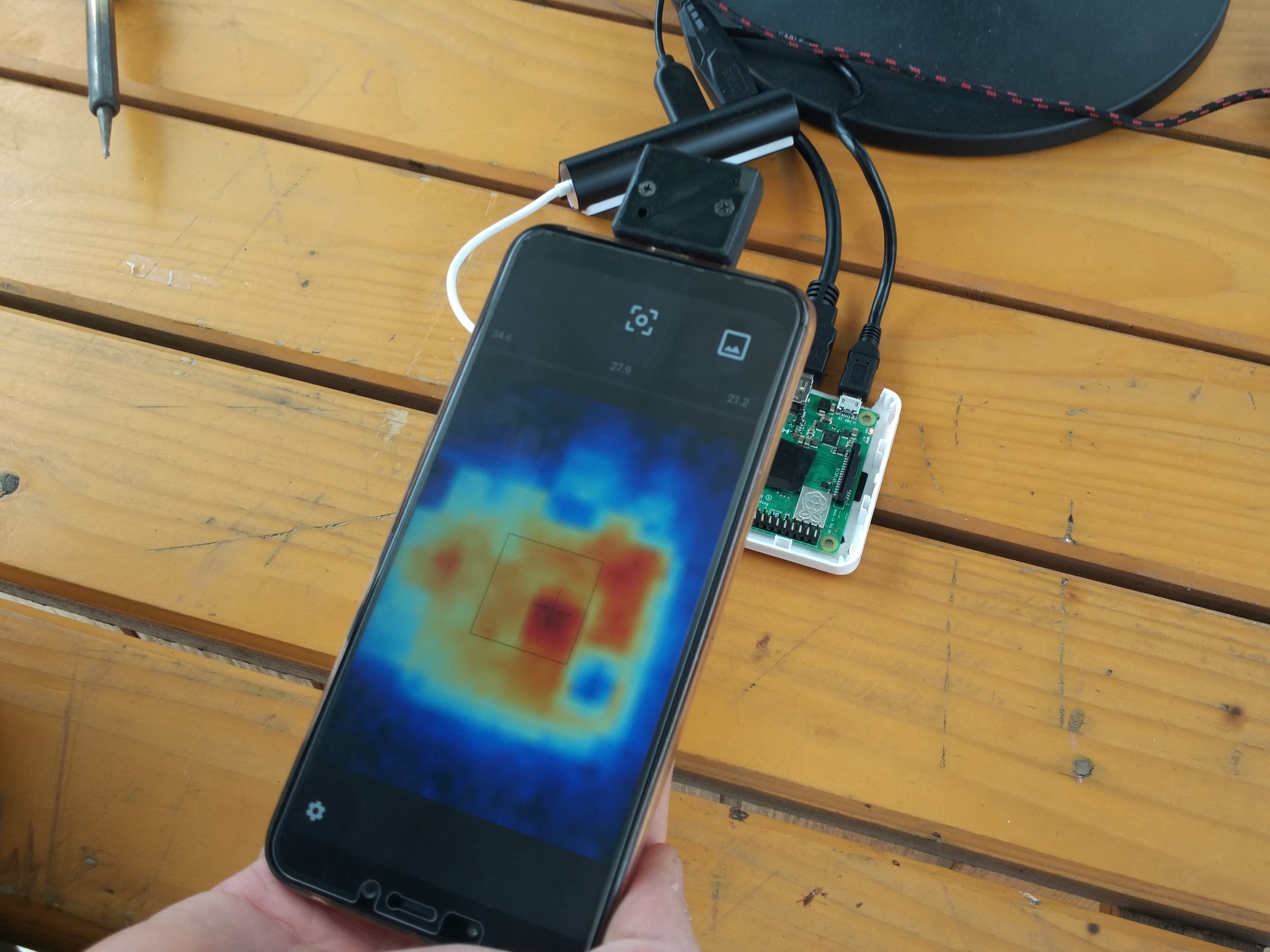
The Open thermal Camera uses the SmartPhone adapter model as it comprises of a thermal camera and a mobile app. The thermal camera is designed to plug into the MicroUSB port on the phone, with a new release of the thermal camera coming with a USB-C option to support phones based on it. With the camera connected, the app is then launched and users can interact with it and evaluate their circuits.
The Open Thermal camera comes in an incredibly small form factor, with all the electronics bumped into an incredibly small 26 x 20 mm PCB. Its design is based on the MLX90640 sensor which is a far-infrared camera with an array of 768 (32×24) thermal sensors that can detect temperatures from -40 to 300°C with approximately 1°C accuracy and up to 64FPS. The camera outputs still images with a resolution of 32 x 24 pixels, and while that might sound quite small and a bit lower than the commercial smartphone adapters, it has been proven to be adequate enough tasks like detecting faults and characterizing a PCB’s thermal performance.
Comparing with the commercial options which fall between $200 and $300 price tags, a look at the BOM of the thermal camera reveals an estimate of only $54 as the cost of its active components with $50 of that cost being the cost of the MLX90640 itself.
Currently, only an Android application based version is available, but according to comments by TheMarpe, there may be plans to support development boards like the Raspberry Pi and other SBCs or a move towards a standalone version.
All project files including the Android app, the KiCad schematics, PCB files, and code to create your own Open Thermal Camera can be found on the project’s GitHub page.
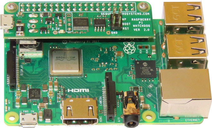
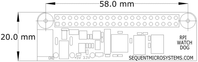
For anyone who loves the Raspberry Pi (I’d imagine everyone does), one of the greatest pain points during the use of it is related in one way or the other to Powering the Pi. From being able to find the right power supply for it, to be able to perform simple actions like resetting the Pi when things get “frozen”, without totally disconnecting it from power. The later can be quite annoying as the use of certain software fixes sometimes doesn’t work. To solve this problem, Sequent Microsystems recently announced the launch of a Hardware Watchdog HAT which is designed to protect the Raspberry Pi from software freezes and also doubling as a power manager for the Raspberry Pi.
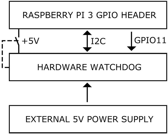
The Hardware Watchdog HAT and Power Manager which comes pin-compatible with all Raspberry Pis with the (now, almost standard) 40-pin connector, features a pair of power connectors including a micro USB port located at the top of the board, and a 2.1mm barrel jack at the bottom. According to Sequent, these ports are to be used to provide power to the raspberry pi and connected peripherals. This means that for the hat to be effective, power must be supplied through the ports on it rather than through the raspberry pi’s USB input. The reason for this is that:
“Since the watchdog can interrupt the power supply to the Raspberry Pi, the supply source needs to be connected to the watchdog”.
The watchdog becomes operational immediately after the Raspberry Pi’s power-up and unless it receives a reset, after 120 seconds, it will cycle the Raspberry Pi power. The watchdog reset is achieved by either sending a command from a memory-resident script or via a Cron job through the I2C port of the Pi or by toggling a GPIO pin. Detailed usage procedure and examples are provided in the User’s Guide.
As mentioned earlier, asides from ensuring the software freezes are not experienced by the Pi, the watchdog also works as a power manager. With this feature, users can program the Raspberry Pi to shut itself down at a scheduled time and program the watchdog to power the Pi up at a later time. This is particularly useful in a portable installation where the Raspberry Pi is powered by batteries, as the watchdog will let you check the power supply voltage, and you can decide to shut down when the level drops below a set value.
The watchdog is probably the smallest HAT (Hardware Attached on Top) in the world, measuring only 65mm x 20mm. It requires less than 5mA to operate and if your application has multiple stack-able boards which need more than the 1.5A that can be supplied by the micro-USB connector or a secondary 2.1mm barrel connector which can supply another 2A.
No Price has yet been placed on the watchdog, but Sequent is currently running a Kickstarter campaign to facilitate the production of the board. More info about the Watchdog can be found on the Campaign page and on Github.
The supplier of complete solutions for display technology, power, and embedded systems, Fortec Electronik, now offers iBASE’s IB818, a single board computer (SBC) expanded to plug-and-play TFT display kit. According to the company, the iBASE IB818 single board computer already configured for display will help facilitate a quick and fast project start upon delivery. Users only need to plug it in and get started immediately.
The iBASE IB818 which measures 102 x 147 mm (4” x 5.8”) is complemented with accessories such as display, cables, memory and SSD disk etc. Among its many features, the single board computer configured to initiate a fast project start includes an SBC display kit with Tiamma and AUO in diagonals from 7 to 24 inches, two SATA III interfaces, two Gigabit LAN (Intel I210IT PCI-E and I211AT PCI-E) for ethernet, an installed AMI BIOS chip, an Intel SoC integrated Gen9 18EUs graphics and, an HDMI 1.4b display and two 24-bit dual LVDS (18/24bit) interfaces for video output. The board is also configured to run on the Intel Celeron N3350 processor 4GB DDR3L RAM and has a 32GB mSATA SSD memory for external storage.
The 3.5-inch disk-size single-board computer expanded to a plug-and-play kit has four USB 3.0 onboard ports, two USB 2.0 ports via pin-header, one RS232/422/485 (jumperless selection) and three RS232 serial ports. It also has 2 mini slot types (2 Mini PCI-E, one full and one half-size), an H/W monitor and a watchdog timer of 256 levels. It is conditioned to operate on a wide temperature range and under a relative humidity of 90% (non-condensing at 60oC).
IB818 is widely applicable in various fields – the medical world, the industrial Internet of Things (IoT), the automation and factory space, with self-service machines and point-of-sale systems, measuring systems and even in the transport field. However, there would not be any scarcity or shortage in supply of this kit in the near future as iBASE has guaranteed a long term availability for the kit.
Meanwhile, all accessories for the IB818 kit has been tested and approved for immediate use by Fortec. Fortec also makes samples available from stock and supplies the IB818F with the displays, accessories and the pre-installed Windows operating system on a project base. User’s manual and datasheet can be downloaded from IBase’s website.
Fortec can be contacted through their various offices in Germany, Switzerland, UK, and USA. For more information on the product and its supplies, you can visit www.fortecag.de
A window detector circuit, also called window comparator circuit or dual edge limit detector circuit is used to determine whether an unknown input is between two precise reference threshold voltages. It employs two comparators to detect over-voltage or under-voltage condition.
This circuit utilizes two comparators in parallel to determine if a signal is between two reference voltages. If the signal is within the window, the output is low thus RELAY is in off condition and also LED is off. Relay provides normally ON and normally OFF switch. If the signal level is outside of the window, the output is high and Relay is in ON condition. For this design, the reference voltages are generated with help of two Trimmer potentiometer. One pot used to set the high voltage level and another one to set the low level voltage adjust. LM358 op-amp used as comparator, it circuit works with 12V DC supply and consumes 50mA current when Relay is in ON state.
Class A amplifiers offer a very good linearity of the output, meaning that the signal is faithfully reproduced, however their efficiency is very low, around 20-30 % in most of the cases. On the other hand, class B amplifiers present a very high efficiency up to 78.5 % but cannot reproduce the output faithfully. Indeed, a crossover distortion appears in a push-pull configuration and the use of a negative feedback is required to limit this effect.
In order to combine both the excellent linearity of class A and the high efficiency of class B, the class AB has been developed. In the very first section, we will present the general functioning and characteristics of class AB amplifiers. Thereafter, we will discuss the efficiency of class AB configurations. The following section will present some possible biasing methods and we will highlight that the diode biasing is the most appropriate. Finally we will see that even the diode biasing method needs to be improved in order for the class AB configuration to correctly amplify the signal with no crossover distortion.
Presentation of the Class AB amplification
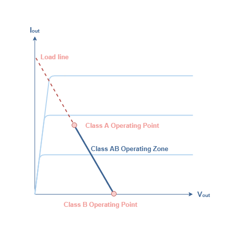
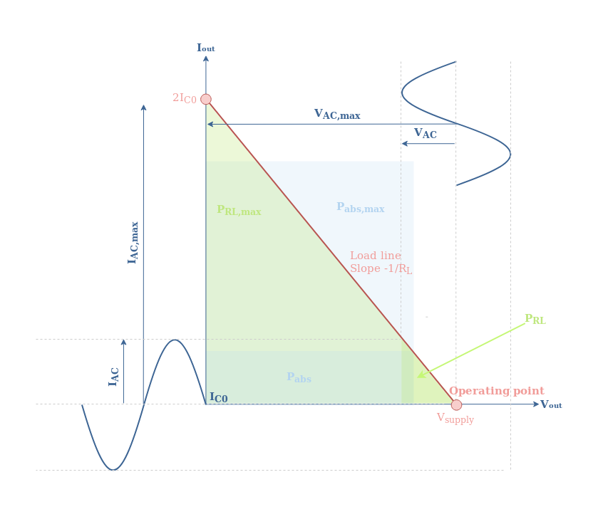
As the name refers to, class AB is working half way between class A and class B amplifiers. The Figure 1 below shows the operating zone of class AB amplifiers in a (Vout,Iout) characteristic graph.
fig 1 : Operating zone of class AB amplifiers
Class AB amplifiers can be biased by choosing an operating point along this blue line, excluding the class A and class B biasing points. The choice of its location depends on the desired levels of efficiency and linearity. If the class AB operating point is closer to the class A operating point (resp. class B) than the class B operating point (resp. class A) the circuit will behave more such as a class A amplifier (resp. class B) by presenting a higher linearity but a lower efficiency (resp. higher efficiency but lower linearity).
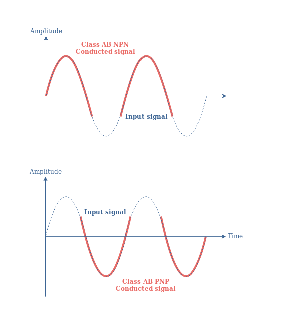
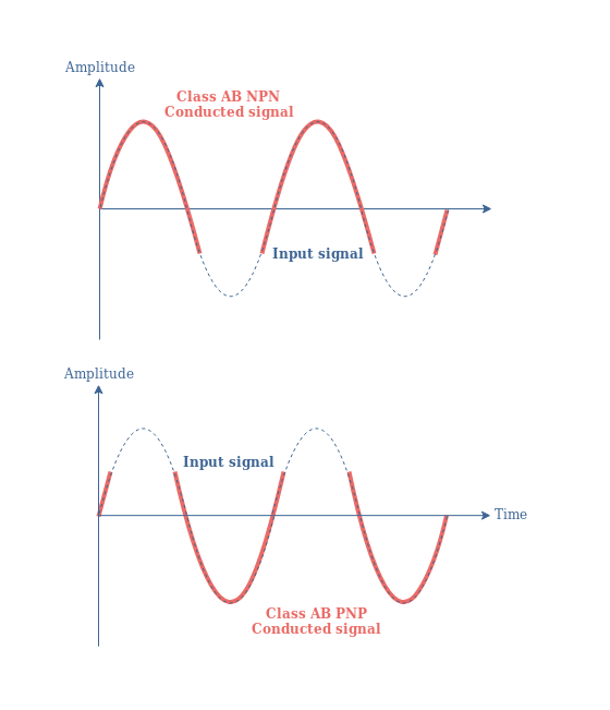
The conduction angle of class AB amplifiers is therefore in the ]180°,360°[ range. This type of amplifier conducts the signal more than 50 % of the time but less than 100 % such as shown in the Figure 2 below :
fig 2 : NPN and PNP-based class AB amplifier conduction angle
Both NPN and PNP-based class AB behaviors are presented since a push-pull configuration is necessary, such as for the class B amplifier, to combine the positive and negative half-waves in order to reproduce the complete signal.
We can note that a small portion of the signal is conducted simultaneously by the NPN and the PNP transistors. This ensures that no crossover distortion is observed during the amplification performed by class AB amplifiers.
Class AB efficiency
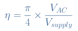
The formula of the efficiency (η) for class AB amplifiers is similar to the class B configuration and is given by the following equation :
eq 1 : Efficiency of a push-pull class AB configuration
Where VAC represents the AC fluctuation of the output signal. The maximum efficiency here, not only depends on the maximized value of VAC, but also on the position of the operating point along the operating zone (see Figure 1) :
If the class AB amplifier is biased at the limit of the cutoff point, VAC,max=Vsupply and thus ηmax=π/4=78.5 %.
If the class AB amplifier is biased at the limit of the class A operating point, VAC,max=Vsupply/2 and thus ηmax=π/8=39.3 %.
In the other cases, the maximum efficiency of a class AB amplifier will be in the ]39.3 % ; 78.5 %[ range.
Biasing methods
There are many ways of biasing a class AB amplifier in order to create an interval of voltage where the complementary transistors conduct simultaneously. In this section, we will briefly present some of the possible biasing methods by highlighting their advantages and disadvantages. The methods will be sorted by how relevant they are, we will indeed begin by the most inappropriate to end with the most common, easier to implement and efficient.
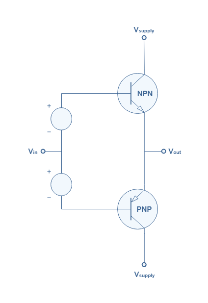
Voltage biasing
A very easy and intuitive method is to bias directly and independently the bases of the NPN and PNP transistors. This supply can be done by batteries or via a DC generator. The output stage of a push-pull configuration that includes this biasing method is shown in the Figure 3 below :
fig 3 : Voltage biasing method
This method has the merit to work but is completely unadapted for real circuits. Indeed, due to packaging and cost constraints, no manufacturer is implementing this solution.
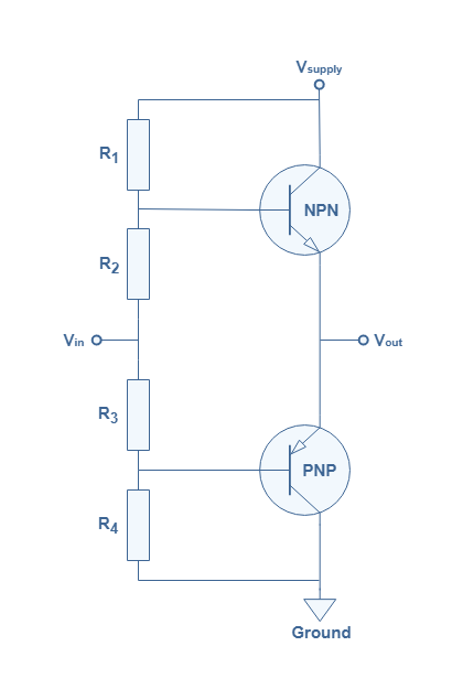
Voltage divider network
This method has been presented many times during the BJT amplifier tutorials and involves only passive components. The Figure 4 below presents a push-pull configuration associated with two voltage divider networks to bias the base of both transistors.
fig 4 : Voltage divider network method
With this configuration, a voltage drop across the two bases (across the total resistance R2+R3) of 1.2 to 1.4 V is observed. This value corresponds to 2×VBE where VBE represents the threshold voltage of the transistors. This voltage drop will bring both transistors above the cutoff state, they will therefore both conduct simultaneously a portion of the input signal.
The main reason why this configuration cannot be used for class AB amplifiers is that the set of values of the resistors will only work for a particular push-pull configuration. Moreover, the set of values needs to be chosen very carefully, specially if the complementary transistors are different.
Potentiometer biasing
This method is very similar to the voltage divider network. The only difference is that an adjustable resistance (or potentiometer) is placed between the two networks. The advantage of this solution is to closely match the biasing of the two complementary transistors with a controllable resistance, even if the transistors have different electrical properties.
However, this solution as well as the voltage divider network involve resistor that generate heat dissipation by Joule’s effect. Since the class AB amplifiers are often biased slightly above the cutoff point to offer a maximum efficiency, any temperature change caused by this phenomenon can result in an inappropriate behavior of the push-pull configuration. This is the reason why diode biasing if often preferred as we will see in the next paragraph.
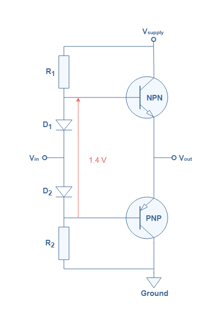
Diode Biasing
Above a certain value of current, diodes have the property to generate a constant voltage drop of ∼0.7 V. It is this feature that is exploited to provide a constant potential of 1.4 V between the two transistor’s bases as shown in the Figure 5 below :
fig 5 : Diode biasing method
Another advantage of this configuration is that the voltage drop across the diodes is self-adjusted with any change of temperature. A rise of temperature will indeed have the effect to decrease the diodes threshold which will decrease the biasing of the transistors and therefore limit a possible thermal runaway.
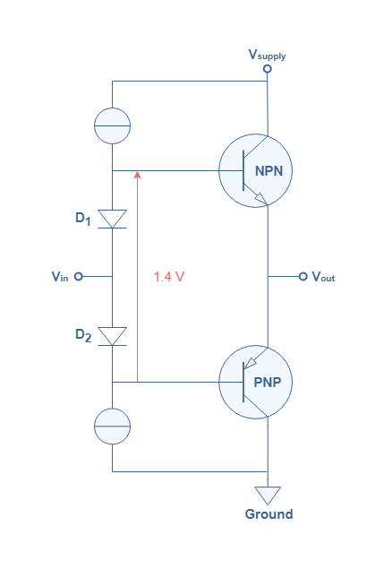
Diode network and current source
The diode biasing circuit, as we just presented before, is the most adapted to bias class AB amplifiers. However biasing directly the diodes with resistances such as presented in Figure 5 leads also to some problems.
The main limitation comes from the resistances R1and R2that bias the diodes. Indeed, if a high output signal is needed, the bases of the transistor will collect all the current from the resistances, therefore the current in the diodes will be zero. Since the diodes receive no current, no bias will be delivered to the push-pull configuration and the crossover distortion will again be observed. This phenomenon is amplified by the fact that when the output voltage increases, the current across the resistances R1 and R2 decreases.
To solve this problem, the resistances are instead replaced with common emitter amplifiers that act as a current sources such as shown in Figure 6. In this case, the current sources can anticipate the variations of the output by providing a constant current as opposition to the resistances. Both the bases and the diodes can therefore be supplied with current.
fig 6 : Diode network and current source method
Power distribution for class AB amplifier
fig 7 : Distribution of power of a class AB amplifier
Conclusion
We have seen that class AB amplifiers contrast with class A and class B amplifiers since they do not have a unique operating point but rather an operating zone delimited by the class A quiescent point and the cutoff point (class B operating point). The location of the operating point along this zone will dictate both the conduction angle and the efficiency of the amplifier.
Indeed, if the class AB operating point is located closer to the class A operating point, the amplifier will have a conduction angle in the [270° ; 360°[ range, therefore conducting more than three quarters of the signal. Moreover, an efficiency in the ]39.3 % ; 58.9 %] interval will be observed.
In the other hand, if the operating point is located closer to the class B operating point, the amplifier will behave more likely as a class B by presenting a lower conduction angle in the interval ]180° ; 270°] which will increase its efficiency between 58.9 % and 78.5 %.
We have seen that a variety of different methods exist in order to bias the bases of a push-pull configuration. We have specifically focused on the voltage biasing, resistor-based biasing and diode biasing. The first one consists of directly biasing the bases with a voltage generator or batteries, but it is not implemented due to costs and packaging problems that arise with it. The second and third methods use voltage divider networks and modified networks with a potentiometer. However, these biasing circuits consist of many resistances and therefore cause heat dissipation that affects directly the behavior of the transistors.
The last method presented can overcome this problem by using a diode divider network. We have indeed seen that this structure creates a constant 1.4 V voltage drop between the two transistor’s bases, which is enough to create an interval where the NPN and PNP transistors conduct simultaneously. Moreover, diodes have the advantages over the resistor to cushion temperature fluctuations.
Finally, we have seen that the diode network must be biased with current sources in order to provide a constant bias to the push-pull configuration bases despite output variations.
The class AB configuration is nowadays the most common in electronic circuits since it combines the advantages of class A and class B amplifiers without their disadvantages.
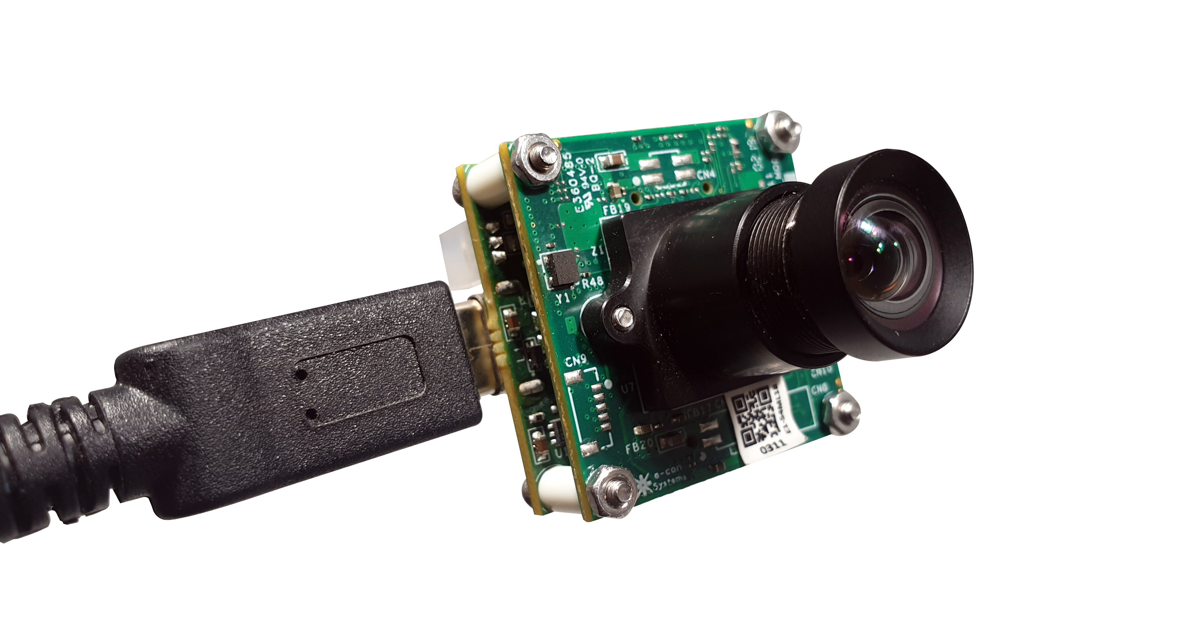
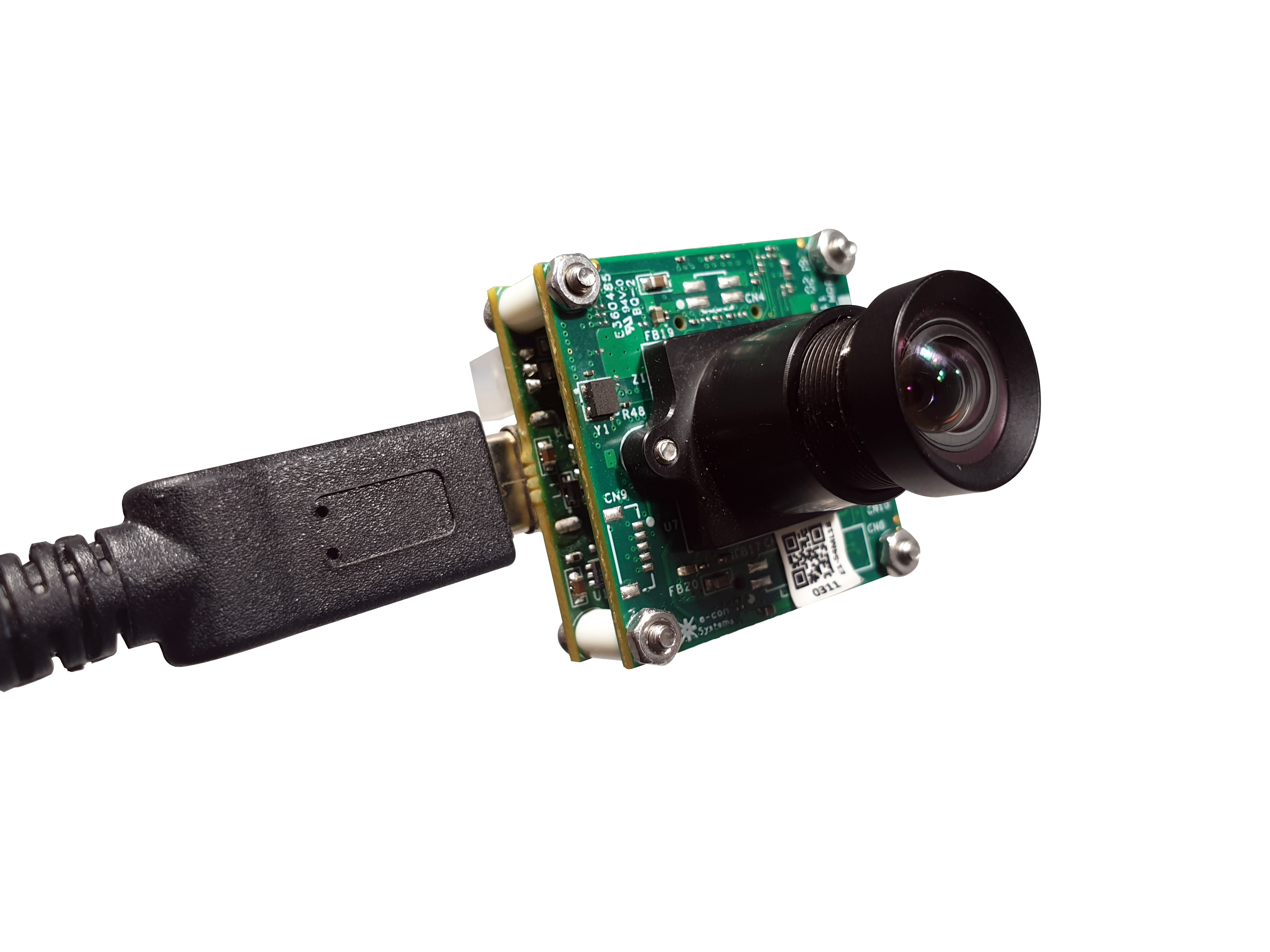
e-con Systems Inc., a leading camera solutions company, today announced the launch of See3CAM_CU55M, a 5 MP Monochrome USB 3.1 Gen 1 SuperSpeed Camera. With a 1/2.5” AR0521 CMOS image sensor from ON Semiconductor, backed by 2.2μm x 2.2μm pixel BSI technology, this camera produces monochrome images of exceptional quality.
See3CAM_CU55M includes a high level of SNR, which guarantees low noise in all conditions. Its Near Infrared (NIR) responsivity ensures amazing image quality in a variety of lighting conditions. See3CAM_CU55M also comes with HD video playback that provides disruption-free streaming capabilities. It is a perfect fit for industries such as Iris and Biometric Authentication, Digital Microscopy, Biomedical Diagnostic Equipment, Barcode Recognition and others.
Fig:1 See3CAM_CU55M – 5MP Monochrome USB 3.1 Gen 1 Camera
“See3CAM_CU55M is e-con’s monochrome counterpart of its successful See3CAM_CU55 camera and it generates excellent images in both visible and Near Infra-red regions”, said Mr. Ashok Babu, President of e-con Systems Inc. “With its low noise and excellent image quality, this will be an ideal camera for applications such as iris recognition, NIR imaging, driver monitoring, digital microscopy etc.,” he added.
The latest Monochrome member of the See3CAM family of USB 3.1 Gen 1 SuperSpeed camera products also comes with S-mount lens holder and a reversible plug and play Type-C connector interface. Supported by native UVC drivers of Windows and Linux Operating Systems (OS), it is a UVC compliant camera and does not require any drivers to be installed on the PC.
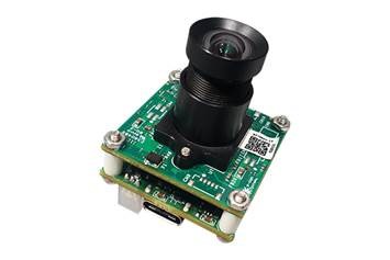
Fig: 2 Microscopy Image of Samples
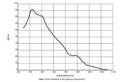
Fig: 3 Quantum Efficiency
Specifications:
Houses e-CAM56_CUMI0521_MOD – 5.0 MP AR0521 Monochrome Camera Module
Fixed Focus with M12 lens holder
Electronic Rolling Shutter
Output format: Y8 (8 bits/pixel) and Y12 (12 bits/pixel)
Plug-and-Play setup (UVC compliant) for Windows 8.1/10 (both 32-bit and 64-bit) and Linux (ubuntu 14.04, 16.04 & 18.04)
Supported OS – Windows 8.1/10 (both 32-bit and 64-bit) and Linux (ubuntu 14.04, 16.04 & 18.04)
USB3.1 Gen1 device with Type C reversible interface connector
Operating Voltage : 5V +/- 5%, Current – 235mA
Operating Temperature Range * : -30°C to 70°C (ambient temperature)
Power requirements:
Max : 1.175W
Min : 0.780W
10 pin GPIO Header
Support for External Hardware Trigger Input
Size in mm (L x W x H) – 30 x 30 x 30.2 mm (without lens)
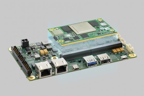
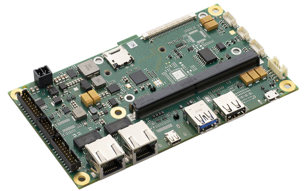
Avnet Integrated announces its second SimpleFlex platform which is well-suited for HMI and IoT applications, and can be quickly adapted to a wide range of other applications with only minor configuration modifications. The ready-to-use SimpleFlex platform MSC SM2S-MB-EP5 is designed for use with Avnet Integrated’s broad portfolio of x86- and ARM-based SMARC 2.0™ modules which encompasses the entire performance range from low power to high performance. Due to to its slim 3.5 inch form factor (146 x 80 mm), the SimpleFlex platform is a perfect fit for modern HMI applications with displays of 7 inches and larger.
The SimpleFlex platform MSC SM2S-MB-EP5 is flexible, comes equipped standard with the SMARC 2.0™ module (according to customer-specific requirements), and is easily configurable without requiring additional development time. More than 30 pre-validated interface combinations are available. There are four variants — two fully equipped platforms and two further optimized platforms with minimum configurations – each for x86- and ARM-based modules.
The SimpleFlex embedded platform is ideally suited for series production and may be ordered in large quantities to support high-volume production runs. Avnet Integrated assembles the application-specific platform in-house on fully automated production lines using state-of-the-art technologies and production processes for reliable implementation of customer-specific applications.
The SMARC 2.0 based SimpleFlex platform can be combined with displays and touch screens from Avnet Integrated to build a complete HMI system. Apart from a wide range of visualization systems and complex display solutions, typical applications include IoT gateways, medical devices, object recognition systems, professional infotainment systems, building automation systems, transportation applications and gaming systems.
Recently Avnet Integrated introduced the SimpleFlex platform MSC Q7-MB-EP5, designed for its modern Qseven™ module families. However, the new MSC SM2S-MB-EP5 platform, according to the SMARC 2.0™ standard, offers significantly more features such as a USB Type-C™ interface with DisplayPort as monitor interface or the connection of fast memory via PCI Express™.
Technical specifications
The SimpleFlex platform MSC SM2S-MB-EP5 embedded platform can be equipped with these modules:
MSC SM2S-IMX8MINI (Mini Cortex™-A53)
MSC SM2S-IMX8M (Cortex™-A53)
MSC SM2S-IMX8 (Cortex™-A72/A53)
MSC SM2S-IMX6 (Cortex™-A9)
MSC SM2S-AL (E3900) and MSC SM2S-ZUSP (Xilinx Zync)
Compatible with many industry-standard interfaces despite its compact dimensions.
Modern monitors can also be connected via DisplayPort and µHDMI, in addition to the USB Type-C™ interface with DisplayPort.
Displays can optionally be controlled via LVDS, MIPI-DSI or eDP.
Up to 2x Gigabit Ethernet, USB 3.0, USB 2.0, 4x UART (as TTL, RS-232 or RS-485), audio with 2.5 W stereo amplifier, MIPI-CSI, GPIO, SPI, I²C and two CAN ports are available, one of which is optionally isolated.
Sockets for Mini PCI Express™, M.2 Key M and Micro-SD can be used to extend the variety of interfaces and memory diversity with fast storage media.
A WLAN/Bluetooth/NFC module with optional antenna additionally ensures the connectivity of the embedded platform.
Designed for use in industrial environments and is specified for the extended temperature range from -40°C to +85°C. Various heat spreaders and heat sinks are available for easy system integration.
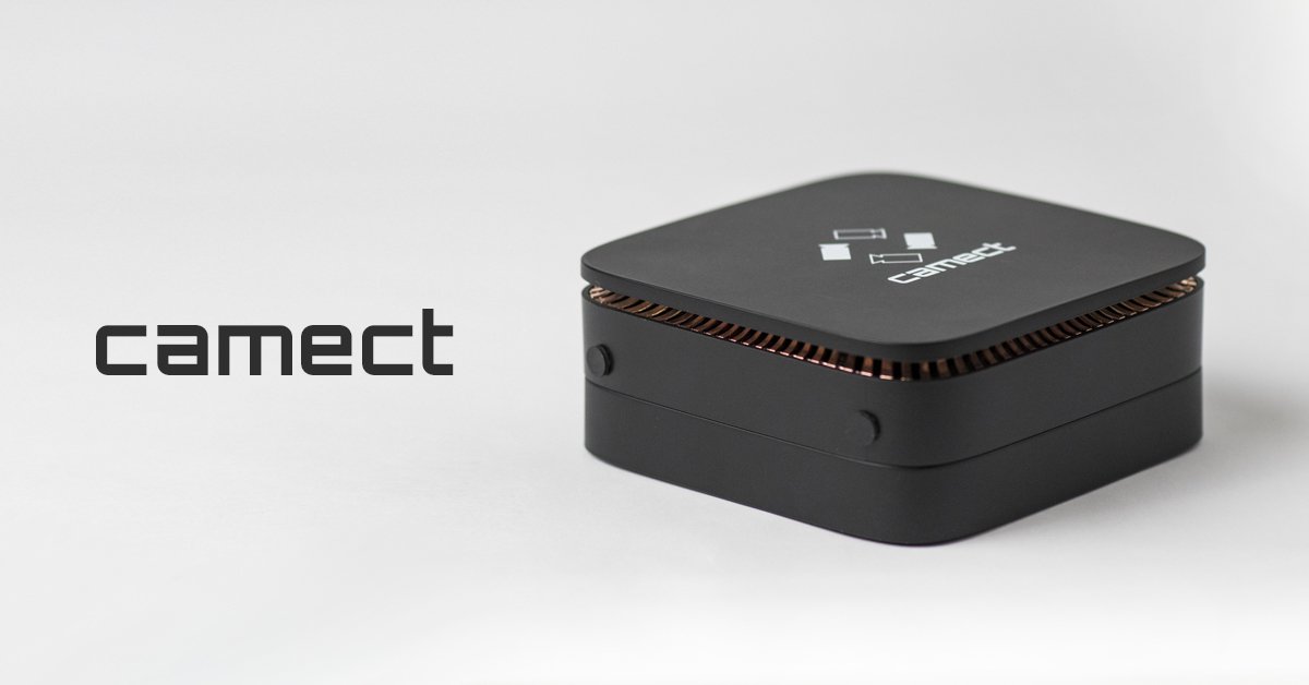
Monitor almost any brand of home security camera from anywhere. Local video storage & AI alerts.
Camect is the only easy, private, smart, and affordable security camera management system that lets you watch what matters most ON YOUR TERMS. Don’t be locked in to proprietary cameras—save on camera costs and high monthly fees! Footage is stored locally, FOR YOUR EYES ONLY.
Works with Most IP Cameras
Easy, Secure Access from Anywhere.
AI-Supported Smart Alerts
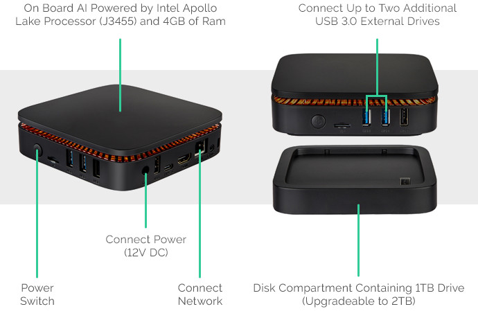
1TB Expandable Storage
One-Plug Network Setup
Optional Cloud Backup
Camect supports about 24M of total camera resolution (e.g. 12 1080p cameras) of average scene complexity.
As Camect records, it applies video analysis to identify motion, a deep learning AI model to identify what’s moving, and your feedback to determine what’s interesting to you. This ensures it delivers the exact alerts you’re looking for.
Camect gets smarter when users choose to share feedback on videos. Providing video examples helps it learn, making it more accurate over time.
Camect adapts alerts based on advanced algorithms and your direct feedback. No more annoying, unneeded alerts – just incredibly accurate ones.
Camect can detect almost 20 more objects than the next most-advanced option, and we’re adding more all the time.
linuxgizmos.com writes:
Camect is not an open source hardware project, but it does offer a path toward hackability. The company has developed an API, which it it has used to implement an “experimental” integration with the Python-oriented Home Assistant home automation platform. Files are posted on GitHub, here and here.
The Camect is available on Indiegogo for another 14 days for $279 or $499 with a lifetime subscription with full Internet services. Otherwise, the subscription starts at $60 per year. More information may be found on the Camect Indiegogo page and Camect website.