Slim Mini-ITX System with AMD Ryzen Embedded V1000 SoC

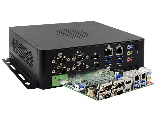
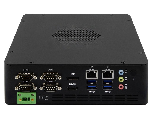
IBASE Technology Inc. (TPEx: 8050), a world leader in the manufacture of industrial motherboard and embedded solutions, today announced the launch of the CMI300-988 slim Mini-ITX system with an onboard AMD RyzenTM Embedded V1807B processor that combines the processing power of the advanced AMD “Zen” CPU and “Vega” graphics architecture in a single chip. Measuring 200 x 200 x 62mm, the CMI300-988 is designed for retail, automation or smart office environments.

Aside from delivering new levels of graphics processing efficiency and superior compute performance, the CMI300-988 combines high-speed connectivity with flexible I/O and high reliability to perform a variety of tasks in 0°C to 45°C operating environments while ensuring silent operation. The embedded box pc adopts an IP30-rated aluminum and steel enclosure, and supports wall mounting as well VESA mounting for easy installation and maintenance. Rear I/O provides essential connections with an HDMI and DisplayPort, two Gigabit Ethernet, four USB 3.1, four serial ports, audio jacks and a 3-pin terminal block for 12V~24V DC input.

The standard system configuration contains 128GB of SSD storage, 4GB of DDR 4 memory, expandable to 32GB, and an 84W power adaptor. Expansion ports consist of a Mini PCI-E and an M.2 (M Key:2280) socket. Three reserved antenna holes are available for optional wireless connectivity.

CMI300-988 FEATURES:

  • AMD Ryzen™ Embedded V1807B on board
  • 2x DDR4 SO-DIMM, Max. 32GB
  • Supports HDMI & DisplayPort
  • 2x Gigabit Ethernet, 4x USB 3.1, 4x COM
  • Wall mount kit included, optional VESA mount kit
  • 1x Mini PCI-E socket, 1x M.2 (M-key)
  • Dimensions: 200(W) x 200(D) x 62(H)mm

No pricing or availability information was provided for the CMI300-988. More information may be found in Ibase’s CMI300-988 announcement and product page.

USB Auto MORSE Keyer

USB Morse Keyer is a microcontroller-based auto keyer with following features:

  • USB / straight key / iambic key inputs.
  • Support for both standalone and USB operating modes.
  • 64-character USB typeahead buffer and 6-character Morse key typeahead buffer.
  • Support 5, 10, 15 WPM.
  • 6-page message memory.
  • 1W audio output.
  • Audio and PTT output interfaces.
  • 32-character display.

The USB interface of this unit is designed to work with most of the operating systems. It emulates a virtual serial terminal to transfer keystrokes to the keyer. In most of the operating systems, this interface works without installing any additional device drivers. To submit keystrokes user can use any serial terminal software such as PuTTY, Hyper Terminal, Minicom, etc.

This keyer is designed to work with 7V to 16V DC input voltage. The most recommended working voltage is 9V.

Fig.1 – The top side of the finished Auto keyer PCB.

To reduce the dimension of the PCB this unit is designed with combining both through-hole and surface mount components. To facilitate future upgrades and modifications, the PIC16F886 MCU sticks with the standard 28-pin DIP package.

Fig.2 – The bottom side of the finished Auto keyer PCB.

This is a certified open-source hardware project. All the design files and firmware source code are available at the project repository on GitHub and on downloads below. The project documentation with all the details which including assembly details, firmware uploading, compilation, and usage instructions are available at the project repository’s wiki.

Makerdiary Releases Pitaya Go IoT Development Board Based on Nordic’s nRF52840 SoC

Makerdiary one of the most innovative startups in the IoT devices space which are known for a series of development boards like the nRF53832-MDK V2 IoT module, and the nRF52840 MDK USB dongle, among others, recently launched a new addition to their impressive line of Nordic’s nRF528xx-series of SoCs based IoT devices, called; Pitaya Go IoT Development Board.

Pitaya Go IoT Development Board

The Pitaya Go combines the Nordic’s nRF52840 SoC with an Arm Cortex-M4 (256Kb of RAM/1Mb of Flash) with FPU, and a Microchip’s ATWINC1500B Wi-Fi controller, in a 60.96mm x 25.4mm x 7.6mm package. This combination brings in a wealth of features which drives the array of connectivity options and high performance associated with the Pitaya Go.

Some of the features of the Pitaya Go include;

  • Nordic Semiconductor nRF52840 SoC
    • 64 MHz Arm® Cortex-M4 with FPU
    • 1 MB Flash + 256 KB RAM
    • Bluetooth 5, Bluetooth mesh, Thread, Zigbee, 802.15.4, ANT and 2.4 GHz proprietary
    • Arm TrustZone® Cryptocell 310 Security Subsystem
    • Integrated USB 2.0 Full-speed Controller
    • QSPI/SPI/TWI/I²S/PDM/QDEC/ADC support
    • Integrated NFC-A Tag
  • Microchip ATWINC1500B Wi-Fi Network Controller
    • Shipped with the latest firmware 19.6.1
    • IEEE 802.11 b/g/n 20 MHz (1×1) Solution
    • Extreme low power with Shutdown Control
    • On-Chip Network Stack to Offload MCU
    • Supports Soft-AP
    • Security protocols supported: WPA/WPA2 Personal, TLS/SSL
    • Enterprise Security with WPA/WPA2 (802.11x)
    • Network services: DHCP, DNS, TCP/IP (IPv4), UDP, HTTP, HTTPS, MQTT, etc.
  • 64Mbit ultra-low-power QSPI Flash Memory
  • Integrated Li-Po Battery Charger with Power Path Management
  • Additional NFC-A Tag PCB Antenna
  • User-programmable RGB LED and Buttons
  • Dual Wi-Fi/Bluetooth 2.4G Chip Antennas
  • Reversible USB-C Connector
  • Li-Po Battery Connector
  • Easily expandable dual 14-Pin Header Sockets
  • Measures 2.4″ x 1.0″ x 0.3″ (60.96mm x 25.4mm x 7.6mm)

Rounding out the Pitaya’s features are an integrated Li-Po battery charger (with power path management), additional NFC-A tag PCB antenna, programmable RGB LED and buttons, dual Wi-Fi/Bluetooth 2.4G chip antennas, USB-C port, Li-Po battery connector, and an expandable 14-pin header.

The Pitaya Go is sold for $34.90 on Makerdiary’s product page as a box which includes;

  • 1x Pitaya Go Board
  • 1x NFC PCB Antenna
  • 1x USB-C Cable

The board comes pre-programmed with an Open Bootloader for DFU (Device Firmware Update) and offers an SDW interface (via socket header) to easily program the board with Nordic’s nRF Connect for Desktop and nRF Util tools.

Next-Generation C4Pi Raspberry Pi 4 Thin Client

ClearCube® Technology, Inc. today announced its new “C4Pi Thin Client”, the latest addition to the Raspberry Pi-based Thin Client portfolio, will be available just weeks after VMworld® 2019 US in San Francisco, CA. The release will occur in conjunction with the anticipated availability of Raspberry Pi 4 capable updates from major VDI providers. A step up from the previous generation models, the form factor of the Pi 4 includes new functionalities to accommodate more robust features. Upon the C4Pi’s release, enterprises will receive notable enhancements in connectivity, memory, processor speed, multimedia, and graphics performance to support everyday workflows. These include a 64-bit quad-core processor that runs at 1.5GHz, USB 3 ports, speedy Gigabit Ethernet, 2.4GHz/5GHz wireless LAN, and PoE enabled capability through a separate PoE hat.

The C4Pi delivers faster boot speeds and considerably better performance for CPU-intensive projects involving emulation, networked AI core, smart home hub, and media center usage. It packs enough power to serve as a substitute for a desktop PC, providing a familiar and complete experience like entry-level x86 PCs in a compact, energy-efficient machine.

“We are the first to introduce yet another technological breakthrough, this time in the form of the C4Pi Raspberry Pi 4. It is yet another testament to how consistently we expand our innovative portfolio of Thin Client solutions that dynamically support virtualization deployments” said Doug Layne, VP of Global Sales. “Designed to maximize IT flexibility, efficiency, and mobility, the Raspberry Pi 4 is suitable for industries such as education, retail, banking, healthcare, and call centers. It facilitates robust connectivity and secure data access in a true, enterprise Thin Client that does not demand active configuration or management, hence easing administrator workload” he added.

The new Pi 4 based Thin Client integrates the ultra-secure Virtual & Cloud Desktop Operating System powered by Stratodesk which offers optimized display and provides VMware connectivity through the Blast Extreme protocol. This facilitates connections back to virtual desktops, terminal services, and backend systems, allowing enterprises to reap the advantages of VDI client computing and management instantaneously.

“Stratodesk NoTouch is already widely known as a highly scalable and cost-effective VDI and IoT endpoint OS and enterprise-grade client management suite,” said Silke Telsnig, CMO of Stratodesk. “We are very excited that ClearCube has chosen Stratodesk to power the new C4Pi Raspberry Pi Thin Client, a high-performance and ultra-configurable solution” she added.

Businesses receive ultimate value through the full coverage offered by the versatile C4Pi Thin Client. It incorporates:

  • Dual 4K displays support via two micro-HDMI ports.
  • Increased USB capacity consisting of two USB 2 ports and two USB 3 ports enables blazing data-transfer speeds in time and mission-critical deployments.
  • Enclosed in an official ClearCube-designed metal case, engineered with heat dissipation and maximum ventilation in mind.
  • Gigabit Ethernet offers fast networking and a PoE HAT add-on powers the device using PoE-enabled networks.
  • Dual-band 802.11ac wireless networking and Bluetooth 5.0
  • It is available in three variations, depending on how much RAM administrators require- 1GB, 2GB, or 4GB.

The Raspberry Pi 4 is optimized for desktop virtualization, browser-based applications, and cloud-first business solutions. It charges over the official USB Type C connector which comes with 15.3W maximum power for full transfer of data, audio, and extensive video outputs in all scenarios. Featuring a captive cable, the USB Type-C connector is reversible, which makes it simple for administrators to plug in and play.

For more information, contact ClearCube Technology at www.clearcube.com.

 Download C4Pi Raspberry Pi 4 Thin Client Datasheet.

Ventana GW5913 Single Board Computer

A miniature 35x100mm single board computer with Mini-PCIe, 802.3at GbE Ethernet, Nano-SIM and Peripheral I/O

The GW5913 is a member of the Gateworks 5th generation Ventana family of single board computers targeted for small embedded applications such as IoT Gateways, Man Portable Units (MPUs), Unmanned Aerial Vehicles (UAV) equipment, digital signage, and robotics. The GW5913 features the Freescale™ i.MX6 Dual Core ARM ® Cortex™-A9 SoC processor operating at 800MHz, 512Mbytes of DDR3-800 DRAM, and 256Mbytes of System Flash. A Mini-PCIe expansion socket with nanoSIM support can be used for 802.11abgn radios, 4G/3G/CATM1 cellular modems and other PCI Express peripherals. A 20 pin header supports Digital I/O, Analog Input, TTL Serial, I2C and USB 2.0. The Gateworks System Controller provides embedded features such as real time clock, voltage and temperature monitor, serial EEPROM, programmable pushbutton switch, and advanced power management with programmable board shut-down and wake-up for remote sensor applications. A wide-range DC input power supply provides up to 8W of power to the Mini-PCIe socket for supporting the latest high-power radios. Power is applied through a dedicated connector or an Ethernet jack in an active 802.3af/at Power over Ethernet architecture. OpenWrt and Ubuntu BSPs are supported.

Features

  • Freescale ™ i.MX6 800MHz Dual Core ARM ® Cortex™-A9 SoC Processor
  • 512MB DDR3-800 SDRAM Memory and 256MB Flash System Memory
  • High-Power Gen 2 Mini-PCIe Socket with USB 2.0 and nanoSIM
  • GbE Ethernet Port
  • Digital I/O & Analog Expansion
  • TTL Serial Expansion
  • I2C Expansion
  • USB 2.0 Expansion
  • Real Time Clock with Battery Backup
  • Voltage and Temperature Monitor
  • Serial Configuration EEPROM
  • Programmable Watchdog Timer
  • Optional u-blox GPS Receiver with MMCX or U.FL Antenna Connector
  • 8 to 60VDC Input Voltage Range
  • Power Through Dedicated Connector or Ethernet with 802.3af/at Active PoE
  • 2W@25 ° C Typical Operating Power
  • 8W Available for Mini-PCIe Socket
  • Reverse Voltage Protection
  • -40 ° C to +85 ° C Operating Temperature
  • OpenWrt and Ubuntu Board Support Packages
  • 1 Year Warranty

more information here: www.gateworks.com

Fujitsu Semiconductor Releases World’s Largest Density 8Mbit ReRAM Product from September

Featuring memory with the industry’s smallest read current, optimal for small wearable devices

Fujitsu Semiconductor announced the release of the 8 Mbit ReRAM MB85AS8MT, which has the world’s largest density as a mass-produced ReRAM product, available from September 2019. This ReRAM product was jointly developed with Panasonic Semiconductor Solutions Co..

The MB85AS8MT is an EEPROM-compatible non-volatile memory with SPI-interface that operates with a wide range of power supply voltages from 1.6 V to 3.6 V. One major feature of this memory is an extremely small average current for read operations of 0.15 mA at an operating frequency of 5 MHz. This enables minimal battery consumption when mounted in battery-operated applications with frequent data-read operations.

Since it can be provided in a very small WL-CSP (Wafer Level Chip Size Package), it is optimal for battery-operated small wearable devices such as hearing aids, smart watches, and smart band.

Fujitsu Semiconductor offers various Ferroelectric RAM (FRAM) products featuring higher write endurance and faster write speeds compared to EEPROM and flash memory. Our FRAM products are becoming known as the optimal non-volatile memory for very frequent data logging and for writing data protection against sudden power outages. Meanwhile, some customers have been requesting memory that uses less current for read operations because their applications perform operations with small data write counts and very frequent data reading.

In order to meet such needs, this new non-volatile ReRAM memory has been developed with the two features of “large density enabling byte-access” and “small read current.” This time, our company has newly developed the MB85AS8MT, featuring world-class largest density in the ReRAM family at 8 Mbit. Its electric specifications, such as commands and timings, are compatible with EEPROM products.

Therefore, mounted in battery-operated applications with frequent data-read operations, such as specific program reading or setting data reading, it enables minimal battery consumption due to its very small read current.

The package is an EEPROM-compatible 8-pin small outline package (SOP). In addition, a very small 11-pin WL-CSP package of 2 mm × 3 mm is available for mounting in small wearable devices.

Key Specifications

  • Memory density (configuration): 8 Mbit (1M words × 8 bits)
  • Interface: Serial Peripheral Interface (SPI)
  • Operating power supply voltage: 1.6 V–3.6 V
  • Operating frequency: Maximum 10 MHz
  • Low кead operating current: 0.15 mA (average value at 5 MHz)
  • Write cycle time: 10 ms
  • Page size: 256 bytes
  • Guaranteed write cycles: 1 million cycles
  • Guaranteed read cycles: Unlimited
  • Data retention: 10 years (up to 85 °C)
  • Package: 11-pin WL-CSP, 8-pin SOP

more information: www.fujitsu.com

Intelligent power module reduces power and noise for drives

Mitsubishi Electric has released a new high-performance intelligent power module (IPM), the Super mini DIPIPM Ver.7, featuring reduced radiation noise and low power consumption for the inverter drive systems of air conditioners and other small-capacity motor drives.

The device features a built-in low-noise seventh-generation insulated gate bipolar transistor (IGBT) with a CSTBT structure to reduce radiation noise while still maintaining the low-power consumption level of the Super mini DIPIPM Ver.6.

Module case operation temperature has been raised from 100 to 125ºC and maximum junction temperature has been raised from 150 to 175ºC to expand the heat-dissipation design flexibility of inverter systems. The 24.0×38.0×3.5mm package has a 40A current and is pin compatible with conventional Super mini DIPIPM series.

Mitsubishi Electric – www.MitsubishiElectric.com

Mitsubishi Electric to Launch MelDIR Thermal Diode Infrared Sensor

Accurately detects heat to identify types of heat sources and specific human behavior

Mitsubishi Electric Corporation announced that it will launch the Mitsubishi Electric Diode InfraRed sensor (MelDIR), a thermal sensor for applications in the fields of security, heating, ventilation and air conditioning (HVAC) and smart buildings, on November 1. MelDIR accurately distinguishes between humans and other heat sources and enables the identification of specific human behavior, such as walking, running or raising hands. It delivers high-pixel, high-thermal-resolution images using thermal diode infrared sensor technology that Mitsubishi Electric developed for the Advanced Land Observing Satellite-2 “DAICHI-2” (ALOS-2).

Features

1) High-pixel, high-thermal-resolution images

  • 10 times higher pixel resolution (80×32 pixels) and five times higher thermal resolution of 100 mK, or 0.1 degree Celsius, compared to 16×16 pixel thermopile sensors now sold in the market, using thermal diode infrared sensor technology installed in the Compact InfraRed Camera (CIRC) for observing the earth with the ALOS-2, which Mitsubishi Electric delivered to the Japan Aerospace Exploration Agency in 2014 and is now in operation.
  • Supporting legs, made extra thin thanks to microfabrication technique, convey energy efficiently without releasing heat, enabling more (smaller) pixels to be used for increased resolution.
  • Electrical noise minimized by mounting thermal diode and high-spec amplifier close to each other on same chip, helping to maintain accuracy and achieve high thermal resolution.
  • Enables highly detailed thermal images for distinguishing between humans and other heat sources and for identifying specific human behavior, such as walking, running or raising hands.

2) Compact, space-saving sensor developed with proprietary chip-scale vacuum-sealing technology

  • Package is 80 percent smaller than that of existing sensors thanks to new packaging technology.
  • Proprietary chip-scale packaging technology and vacuum-sealing technology enable sensor to be vacuum sealed (without using conventional ceramic package) to avoid heat radiation and achieve high thermal resolution.

more information: www.mitsubishielectric.com

Microchip’s SAM R30 Sub-GHz Module for Ultra-Low-Power WPAN Designs

Mouser Electronics is now stocking the SAM R30 sub-GHz module from Microchip Technology. The industry’s smallest IEEE 802.15.4-compliant module, the SAM R30 combines an ultra-low-power microcontroller with a sub-GHZ radio in a 12.7 × 11 mm package, enabling long-lasting battery life in space-constrained designs like wireless-networked sensors and controls in home automation, smart city, and industrial applications.

The Microchip SAM R30 module, available from Mouser Electronics, is based on a Microchip SAMR30E18A system-in-package (SiP) with 32-bit Arm® Cortex®-M0+ core and up to 256 Kbytes of flash and 40 Kbytes of RAM. Designed for use in unlicensed sub-1GHz frequency bands worldwide — such as 780 MHz (China), 868 MHz (Europe), and 915 MHz (North America) — the module delivers receive (RX) sensitivity up to -105 dBm and transmit (TX) output power up to +8.7 dBm.

The module offers twice the connectivity range and better communication through walls and floors than similarly powered devices using the 2.4 GHz frequency band. Featuring an ultra-low-power sleep mode of under 800 nA, the SAM R30 module is ideal for Internet of Things (IoT) sensor applications that require long battery life. Further, developers can implement propriety point-to-point, star, or self-healing mesh networks with Microchip’s MiWi™ protocol stack.

Features

  • Compact 802.15.4 Sub-1GHz module
  • ATSAMR30E18A SiP with ARM Cortex-M0+ MCU and Sub-1GHz transceiver
  • Integrated Ultra Low Power Transceiver for 700/800/900MHz ISM band
  • 256KB Flash
  • 16 Input/Output pins
  • Maximum operating frequency 48MHz
  • 128-bit Advanced Encryption Standard (AES) crypto engine
  • 32-bit Medium Access Control (MAC) symbol counter
  • Automatic retransmission modes
  • Single 1.8-3.6V supply
  • FCC / ETSI compliant RF front end with a harmonic filter
  • Two Serial Communication interface (SERCOM) units left for external applications
  • High precision 16MHz crystal oscillator
  • 12-bit, 350ksps Analog-to-Digital Converter (ADC)
  • I2C up to 3.4MHz
  • Full-speed (12Mbps) Universal Serial Bus (USB) 2.0 interface
  • 16 External General Purpose Input/Output (GPIO) lines

Mouser also stocks the SAM R30M Xplained Pro Evaluation Kit, which includes an onboard embedded debugger, QTouch® button, two Xplained Pro extension headers, and embedded current measurement circuitry. The board features both a chip antenna and an SMA connector for an external antenna, a digital temperature sensor, and USB-UART/I2C convertor. The board is supported by the Atmel Studio integrated development platform, which provides predefined application examples.

Both the module and the evaluation kit are certified with the Federal Communications Commission (FCC), Industry Canada (IC), and Radio Equipment Directive (RED), allowing designers to focus on time-to-market instead of RF testing certification costs.

For more information on the SAM R30 module, visit www.mouser.com/microchip-atsamr30m18a-modules.

AI Compute Acceleration Startup Builds the Largest Chip Ever For Deep Learning Applications

To meet the ever-increasing computational demands of AI, California based AI startup, Cerebras Systems, just recently unveiled its very first announced element claimed to be the most massive AI chip ever made. With an astounding measurement of 46,225 mm2 (up to 56.7 times more than the largest graphics processing unit) and more than 1.2 trillion transistors, the Wafer-Scale Engine from Cerebras Systems is the largest semiconductor ever built for deep learning applications.

The Wafer-Scale Engine contains about 400,000 high performance, AI optimized Sparse Linear Algebra cores. This local memory fed cores are linked together by a fine-grained, high bandwidth, all-hardware, low latency mesh communication network at an interconnect speed of 100,000 Pb/s. Unlike other processors and GPUs that are produced on silicon wafers, Cerebras’ WSE is a single chip interconnected in a single wafer designed to handle all its transistors. The WSE also houses on-chip of 18Gb superfast and distributed SRAM memory among the cores in a single-level hierarchy. By way of comparison, the WSE has 3000 more on-chip memory and more than 10,000 times the memory bandwidth.

Designed for accelerating AI work, the company claims that its Wafer-Scale Engine can scale down the time it takes to process complex data from months to minutes.

“Every architectural decision was made to optimize performance for AI work. Designed from the ground up for AI work, the Cerebras WSE contains fundamental innovations that advance the state-of-the-art by solving decades-old technical challenges that limited chip size such as cross – reticle connectivity, yield, power delivery and packaging. The result is that the Cerebras WSE delivers, depending on workload, hundreds or thousands of times the performance of existing solutions at a tiny fraction of the power draw and space,”

says, CEO and Founder of Cerebras Systems, Andrew Feldman.

According to the company, bigger is better; the larger the chips, the less time it takes to process information and produce answers. The performance gain of the Wafer Scale Engine is largely due to its size. With a chip as big as the size of an iPad, the WSE is able to process information more quickly in less time, thus facilitating several AI paradigms like reducing the “time-to-insight” or “training time” within neural network loops. The speed at which a neural network loop is able to learn or train depends on the speed with which inputs move through the loop as such, the faster the inputs are processed through the feedback loop, the more inputs the loop receives per unit time and the faster the loop trains.

Due to its large silicon area, the WSE is able to provide more cores, more memory close to the cores that ensures that the cores are always occupied doing calculations, and more latency bandwidth between the cores for maximum efficiency. The programmable SLA cores are designed fundamentally to handle core neural network workload like TensorFlow, Pytorch and more.

In recent years, we have seen Artificial Intelligence rise from a state of obscurity to top-of-the-mind awareness because of the advances in deep learning. With WSE that help to train models in less time and with less energy, deep learning researchers should be able to explore more ideas, test hypothesis more quickly, use more data and solve new problems.

TOP PCB Companies