Tiny TFT Graphics Library for ATtiny84

This is a graphics library for the family of small colour TFT displays based on the ST7735 and ST7789 driver chips. These are really nice displays; bright, colourful, available in a variety of useful sizes, and available at low cost from suppliers like Adafruit, AliExpress, or Banggood. This is a new project by David Johnson-Davies. He writes:

This library allows you to plot points, draw lines, draw filled rectangles, and plot text with an optional scale factor. I’ve included a demo histogram-plotting program that adjusts itself to fit each of the displays I’ve supported.

Unlike most other TFT display libraries this one doesn’t require a memory buffer, allowing it to be run on any processor down to an ATtiny85. The displays require four pins to drive the display, leaving one pin free on an ATtiny85 to interface to another device, such as a temperature sensor. If you need more pins choose a larger chip, such as the ATtiny84; see Using the library with other AVR chips at the end of the article for information about how to convert the code for different chips.

Tiny TFT Graphics Library for ATtiny84 – [Link]

Congatec boards with 8th Gen Intel® Core™ Mobile processor and 10+ years availability

Up to 58% performance boost with extended availability

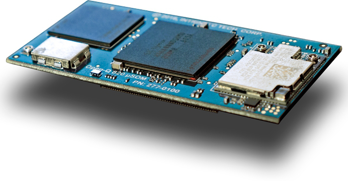
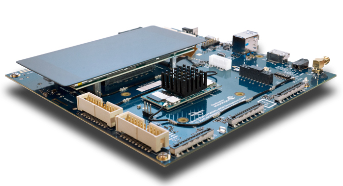
Congatec, a leading vendor of standardized and customized embedded computer boards and modules, announced today that the brand new embedded versions of the 8th Generation Intel® Core™ Mobile processors (codenamed Whiskey Lake) are now available on COM Express Type 6 Compact modules, 3.5 inch SBCs, and Thin Mini-ITX motherboards. OEM customers benefit from an instant performance boost of up to 58%¹ compared to previous embedded U-Series processors – enabled by 4 instead of 2 cores plus an overall improved microarchitecture. Thanks to features such as optional Intel® Optane™ memory 2 or USB 3.1 Gen2, everyday tasks are even more responsive. The processor cores allow efficient task scheduling and furthermore support the use of the RTS hypervisor software to allow additional optimization of I/O throughput from the input channels to the processor cores.

The new Congatec boards run Linux, Windows 10, or Win 10 IoT Enterprise on the following processors:

  • Core i5-8365UE (4x cores @ 1.6GHz, 6MB cache, 15W)
  • Core i7-8665UE (4x cores @ 1.7GHz, 8MB cache, 15W)
  • Core i3-8145UE (2x cores @ 2.2GHz, 4MB cache, 15W)
  • Celeron 4305UE (2x cores @ 2.0GHz, 2MB cache, 15W)

Designed for harsh and space-constrained environments, the new high-end Intel® Core™ i7, Core™ i5, Core™ i3 and Celeron® embedded processor boards and modules are the first in the industry to offer long-term availability of 10+ years. This brand new embedded x86 design principle premiers at congatec and within the entire embedded board vendor space² with the launch of the new 8th Generation Intel® Core™ Mobile processor boards. Addressing in particular the increased life cycle needs of the transportation and mobility sector, these new boards and modules are also a perfect fit for all other embedded applications – such as medical equipment and industrial controls, embedded edge clients and HMIs – as they enable extended life cycles without additional costs for customers.

“One of our main goals is to simplify the use of embedded computer technology as much as possible for our OEM customers. That’s why we offer our brand new 8th Gen Intel® Core™ Mobile processor based embedded boards and modules now with 10+ and on basis of specific last time buy contract up to 15 years long-term availability right from the start, as 7 years are often insufficient for many high-end embedded computing sectors. Our extended life cycle – which, by the way, comes without additional costs – thus helps OEMs to extend their own product life cycles for an even better ROI,” explains Christian Eder, Director of Marketing at congatec.

In the past, many high-end embedded applications tended towards life cycles shorter than 7 years, as they often required a new performance boost from next generation processors before then. But with increased certification demands in several new embedded application areas such as mobile vehicles, OEMs are similarly keen on longer life cycles today. Extending the life cycles of standard embedded x86 platforms to 10 or even 15 years off the shelf is consequently a major bonus for customers across the entire embedded computing market.

“We are very happy to get our hands on embedded versions of this brand new Intel architecture with 10+ year long-term availability. Longer life cycles are a key requirement in many mobile applications we target in rugged environments, where high speed data streams need to be acquired and logged for 3D object recognition, lidar imaging, and mobile mapping. The same requirement that our end customers expect from our data recorders used for wireless network monitoring and automotive test systems or data loggers for test vehicles which store and analyze high speed data streams from external sensors on solid state drives or hard drives,” explains Thomas Hagios, CEO of MCTX Mobile & Embedded Computers GmbH.

The feature set in detail

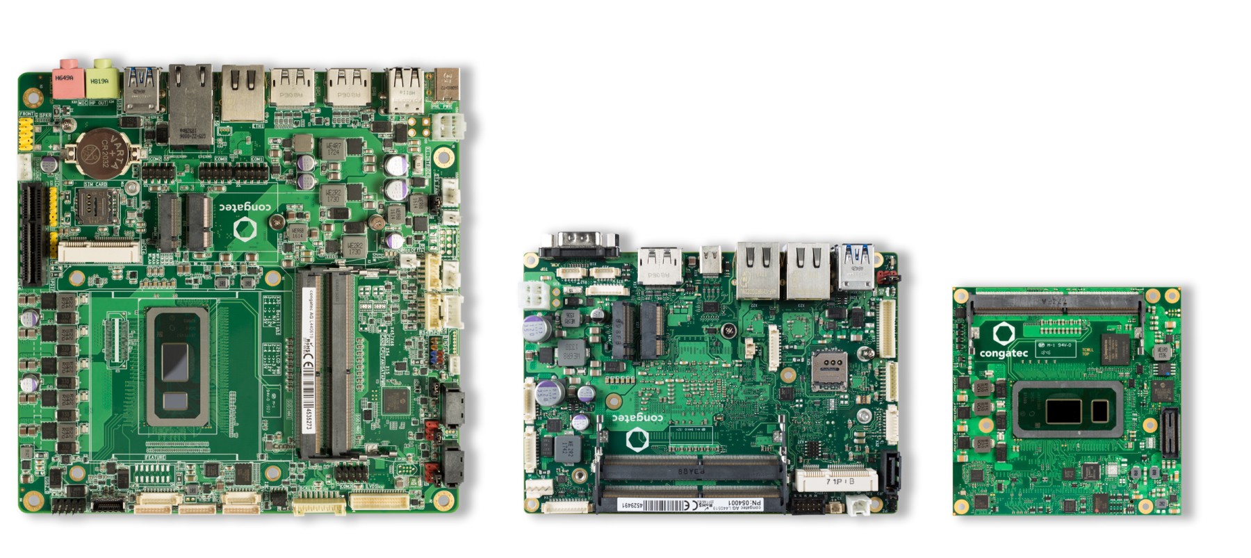
The new conga-TC370 COM Express Type 6 modules, the conga-JC370 embedded 3.5 inch SBCs, and the conga-IC370 Thin Mini-ITX motherboards all feature the latest Intel® Core™ i7, Core™ i5, Core™ i3 and Celeron embedded processors with a long-term availability of 15 years. The memory is designed to match the demands of consolidating multi OS applications on a single platform: Two DDR4 SODIMM sockets with up to 2400 MT/s are available for a total of up to 64GB. For the first time, USB 3.1 Gen2 with transfer rates of 10 Gbps is now supported natively, which makes it possible to transfer even uncompressed UHD video from a USB camera or any other vision sensor. The new 3.5 inch SBCs provide this performance via a USB-C connector that also supports 1x DisplayPort++ and power supply for peripheral devices, thereby enabling monitor connection with a single cable for video, touch and power. The COM Express modules support the same feature set on carrier boards. Further interfaces depend on the form factor, but all support a total of 3 independent 60Hz UHD displays with up to 4096×2304 pixels as well as 1x Gigabit Ethernet (1x with TSN support). The new boards and modules offer all this and many more interfaces with an economical 15W TDP that is scalable from 10W (800 MHz) to 25W (up to 4.6 GHz in Turbo Boost mode).

The Conga-TC370, Conga-JC370, and Conga-IC370 are available now, with pricing undisclosed.

more information: www.congatec.com

The MAX77860 is a USB type-c, 3A switch-mode buck charger with integrated CC detection, reverse boost, and ADC.

Ease of design and 30 percent smaller design size, with the MAX77860.

The MAX77860 is a high-performance single input switch mode charger that features USB Type-C CC detection capability in addition to reverse boost capability and a Safeout LDO.

This switched-mode battery charger with two integrated switches, provides small inductor and capacitor sizes, programmable battery charging current. It is ideally suited for portable devices such as smartphones, IoT devices, and other Li-ion battery powered electronics, featuring a single input, which works for both USB and high voltage adapters. It supports USB Type-C CC detection under BC 1.2 specification, and the power-path switch is integrated in the chip. All MAX77860 blocks connected to the adapter/USB pin are protected from input overvoltage events up to 14V.

The switching charger is designed with a special CC, CV, and die temperature regulation algorithm, as well as I2C programmable settings to accommodate a wide range of battery sizes and system loads. Additionally, the on-chip ADC can help monitor the charging input voltage/current, battery voltage, charging/discharging current, and the battery temperature.

— Win a free evaluation kit —

Applications

  • USB Type-C Charging for 1S Li-ion Applications
  • Mobile Point-of-Sale Devices
  • Portable Medical Equipment
  • Portable Industrial Equipment

Key features

  • Single-Input Switch Mode Charger
    • Up to 14V Protection
    • 4.0V to 13.5V Input Operating Range
    • Switching Charger with D+/D- Charger Detection
    • Up to 4.0A Input Current Limit with Adaptive Input Current Limit (AICL)
    • Up to 3.15A Battery Charging Current Limit
    • Optional External Sense Resistor
    • CC, CV, and Die Temperature Control
    • Supports USB-OTG Reverse Boost, up to 1.5A Current Limit
    • Master-Slave Charging Capability, up to 6A Charge Current
    • Integrated Battery True-Disconnect FET
    • Rated up to 9ARMS, Discharge Current Limit (Programmable)
  • USB Type-C Detection
    • Integrated VCONN Switch
    • CC Pin
    • D+/D- Detection for USB HVDCP
    • BC 1.2 Support
  • One Safeout LDO
  • I2C-Compatible Interface

… read more

Low Dropout (LDO) Linear Regulators Selection Guide from Analog Devices [PDF]

Analog Devices’ Power by Linear™ product group produces a broad line of high performance low dropout (LDO) linear regulators. These LDOs offer very low dropout, fast transient response, excellent line and load regulation, and feature a very wide input voltage range from 0.9 V to 80 V. Output currents range from 100 mA to 10 A, with positive, negative and multiple outputs. Many devices offer output voltage operation <0.8 V and some feature operation down to as low as 0 V even with single-supply operation. Many are stable with ceramic output capacitors. These devices can be designed into virtually any end application and market segment.

Low Dropout (LDO) Linear Regulators Selection Guide from Analog Devices – [PDF]

0.86″ 96×32 White Graphic OLED Display Module

This is a 0.86″ 96×32 White Graphic OLED Display Module supporting SPI,MCU,I2C

Main features

  • 0.86″
  • 96 X 32 Pixel
  • CPU Interface: 8-bit 6800/8080 Parallel, 4-wire SPI, 3-wire SPI, I2C (default)
  • Drive IC: SSD1316
  • Display Colors :White
  • Graphic OLED

The OLED module is available from www.displaymodule.com for $7.95

Intrinsyc Announces Immediate Availability of the Open-Q™ 820Pro High-Performance System on Module

High-performance edge computing module for use in a variety of consumer and industrial IoT Devices

Intrinsyc Technologies Corporation, a leading provider of solutions for the development and production of embedded and Internet of Things (IoT) products, today announced the availability of the Open-Q™ 820Pro µSOM (micro System on Module) and Development Kit.

Open-Q 820Pro µSOM Development Kit

Intrinsyc’s Open-Q™ 820Pro µSOM (micro System on Chip) provides an enhanced power-performance combination from our popular 820 µSOM, with increased processing power, more memory, and long-life availability, in the same ultra-compact 25×50 mm form factor. The production ready, pre-certified 820Pro µSOM is a pin compatible, drop-in replacement for the existing 820 µSOM, requiring only SW changes to provide higher performance, with more efficiency, and long-term availability. With 9% faster CPU and 5% faster GPU speeds at the same power consumption, combined with 33% more RAM, the 820Pro µSOM can provide either more processing power for your demanding applications, or lower average power consumption for the same processing tasks.

“We are excited to introduce this enhanced edge computing module, with premium performance features and long-life support” said Cliff Morton, Vice President, Solutions Engineering, Intrinsyc.  “We’ve designed the new module to facilitate a smooth upgrade path for existing users of our popular 820 µSOM, and new clients will be able to accelerate time to market with our flexible development kit and pre-certified production-ready module; with the assurance of long-term availability and support.”

Open-Q™ 820Pro µSOM Specifications:

  • Qualcomm® Snapdragon™ 820E (APQ8096SG) Application Processor
    • Qualcomm® Kryo™ Quad-Core 64-bit CPU: @ up to 2.342 GHz
    • Qualcomm® Adreno™ 530 GPU @ 652.8 MHz
    • Qualcomm® Hexagon™ 680 DSP @ 825 MHz
  • System Memory: 4GB LPDDR4 SDRAM (PoP) + 32GB UFS flash storage
  • Wireless Connectivity: Wi-Fi 802.11a/b/g/n/ac 2.4/5Ghz 2×2 MU-MIMO + Bluetooth 4.2
  • Display Interfaces:
    • HDMI 2.0 – 4K UHD at 60fps
    • 2x MIPI 4-lane DSI + touch panel
  • Camera Interfaces:
    • 3x MIPI CSI camera ports
    • Qualcomm® Spectra™ 180 dual 14-bit ISP – up to 28MP cameras
  • Video Performance:
    • 264 (AVC): Video Playback and Capture at 4K60
    • 265 (HEVC): Video Playback at 4K60 and video capture at 4K30
  • Audio Interfaces:
    • SLIMBus to support Qualcomm® WCD9335 audio codec (off-SOM)
    • Multi-channel I2S digital audio interfaces
  • I/O Interfaces:
    • 1x USB 3.0 device or host, 1x USB2.0 device or host
    • 1x USB 2.0 micro-B (debug UART)
    • 1x SDIO 4-bit interface
    • 2x PCIe v2.1 interface
    • Sensor interface – SPI, UART, I2C to sensor DSP core
  • Power: Integrated battery management on SOM
  • Size: 25mm x 50mm x 4.5mm
  • Operating Systems: Android™ 9, Debian Linux

Additional information is available at:

https://www.intrinsyc.com/computing-platforms/open-q-820Pro-usom-system-on-module-som

To help IoT device makers accelerate time to market, Intrinsyc offers the Open-Q™ 820Pro µSOM Development Kit, as well as turnkey product development services, driver and application software development, technical support, and documentation.

Intrinsyc’s Open-Q™ 820Pro µSOM Development Kit is a full-featured development platform including the software tools and accessories required to immediately begin development.  The development kit marries the production-ready Open‐Q™ 820Pro µSOM with an open-frame development platform providing numerous expansion and connectivity options. The Dev Kit and SW packages support the development and testing of a wide variety of peripherals and applications, ensuring the fastest time to market possible. The Development Kit is available for purchase at:

https://shop.intrinsyc.com/products/open-q-820Pro-usom-development-kit

High-performance ARM SoM Powered by NXP i.MX 8M

Shenzhen, China – June 11, 2019 – MYIR introduces a high-performance ARM SoM MYC-JX8MX CPU Module, which is built around the NXP i.MX 8M Quad processor featuring 1.3GHz quad ARM Cortex-A53 cores and a real-time ARM Cortex-M4 co-processor. The module runs Linux and is capable of working in extended temperature ranging from -30°C to 80°C.

Measuring 82mm by 52mm, the MYC-JX8MX CPU Module has integrated 1GB/2GB LPDDR4, 8GB eMMC, 256Mbit QSPI Flash, Gigabit Ethernet PHY and PMIC on board. A large number of I/O signals are carried to or from the i.MX 8M CPU Module through one 0.5mm pitch 314-pin MXM 3.0 expansion connector, making it an excellent embedded solution for Scanning/Imaging, Building Automation and Smart Home, Human Machine Interface (HMI), Machine Vision and more other consumer and industrial applications which requires high multi-media performance.

MYC-JX8MX CPU Module (delivered with heat sink by default)

MYIR also offers a versatile platform MYD-JX8MX development board for evaluating the MYC-JX8MX CPU Module. It takes full features of the i.MX 8M processor and has brought out rich peripherals through connectors and headers such as 4 x USB 3.0 Host ports and 1 x USB 3.0 Host/Device port, Gigabit Ethernet, TF card slot, USB based Mini PCIe interface for 4G LTE Module, WiFi/BT, Audio In/Out, HDMI, 2 x MIPI-CSI, MIPI-DSI, 2 x LVDS display interfaces, PCIe 3.0 (x4) NVMe SSD Interface, etc. It is delivered with necessary cable accessories for customer to easily start development as soon as getting it out-of-box.

MYC-JX8MX block diagram

Features

Mechanical Parameters

  • Dimensions: 50mm x 82mm
  • PCB Layers: 10-layer design
  • Power supply: +5V/0.5A
  • Working temperature: -30~80 Celsius

Processor

  • NXP i.MX 8M Quad Processor based on 1.3GHz Quad ARM Cortex-A53 and 266MHz Cortex-M4 cores
    (MIMX8MQ6CVAHZAB by default)

Memory

  • 1GB / 2 GB LPDDR4 (supports up to 4GB LPDDR4)
  • 8GB eMMC Flash (supports up to 64GB eMMC)
  • 256Mbit QSPI Flash

Peripherals and Signals Routed to Pins

  • One 10/100/1000Mbps Ethernet PHY
  • Power Management IC (ROHM BD71837MWV)
  • 0.5mm pitch 314-pin MXM 3.0 Expansion Connector
    – 1 x 10/100/1000Mbps Ethernet
    – 3 x Serial ports
    – 3 x I2C
    – 2 x SPI
    – 4 x PWM
    – 3 x USB 3.0
    – 2 x PCIe
    – 6 x I2S / SAI
    – 2 x MIPI Camera Sensor Interface
    – 1 x JTAG
    – 1 x HDMI 2.0a output
    – Up to 108 GPIOs
MYD-JX8MX Development Board


MYD-JX8MX block diagram

MYIR offers 1GB or 2GB RAM selections for the CPU modules and development boards which have very-high powered prices to compare.

More information about the new products can be found at:

HT-102 – A Thermal Camera On A Budget

Thermal Camera records infrared images that the human eyes can’t see which can give it a niche use for different applications. A thermal camera is great of observing the temperature variation of an object and it has application in the health, security, electronics, animal and several industries. The most critical parameter for the thermal camera is its temperature sensitivity, the more sensitive a thermal camera is, the best the quality of the image, which usually translates to better measurement.

HT-102 Thermal Camera

With a thermal camera, you can see things at night like people moving around because they have apparent temperature variation of body temperature. One exciting application of thermal imaging I like is the ability to see what may be happened in”Past.” Thermal imaging of an object or place can give a hint of what might have happened at some time t – 1, for example, in a parking lot, thermal imaging of the cars will tell you which car was recently driven or if someone once moved around that place.

Although thermal imaging application sounds pretty cool, one of the challenges of using Thermal cameras is the relatively high cost of getting the cameras. The thermal cameras could cost up to thousands of dollars; they are usually expensive. One way to buy a lower cost thermal camera, is to get those that need to be used with a smartphone which does cost around $200 on Amazon. A very cheap one discovered is the HT-102 thermal camera designed to work with Android Phones.

HT-102 Thermal Camera

The HT-102 is a Chinese made thermal camera available for about $120 on Gearbest.The HT-102 thermal camera can be connected to your smartphone (Android supported) and used to take thermal imaging of the environment. Below are some of the device specifications:

  • Material: metal
  • Capture Temperature Range – -20 to 300°C
  • Accuracy – ±3℃ or ±5% of reading
  • Resolution – 0.1℃ or 0.1℉
  • Working band – 8-14μm
  • Horizontal viewing angle / vertical viewing angle – 43°±1°/ 43°±1°
  • Infrared image resolution – 32 x 32
  • Visible image resolution – 640 x 480
  • Phone I/F – USB type-C port for data and power
  • Dimensions – 60  x 30 mm
  • Weight – 19 grams
  • Temperature Range – Operating: 0 to 35°C; storage: -20 to 60°C

The camera ships with an English user manual, a storage box, and a USB Type-C to Micro USB Adapter for phones without a USB-C port. The camera requires the Thermal Viewer app for Android to be able to be used and visualize the result. Below is a sample of the possible output you will get with the camera.

HT-102 Thermal Camera With Thermal Viewer App

Although, the HT-102 is a sizeable and low-budget thermal camera don’t expect it to stand toe to toe with higher end thermal cameras like those from FLIR cameras and others. HT-102 is a basic thermal camera to get started with loving thermal imaging. A quick search on Aliexpress also shows a similar like HT 102 that cost rough around $96.

Toshiba launches new family of low voltage driven photorelays

Toshiba Electronics Europe GmbH, the industry leader in the miniaturisation of cutting-edge photorelays, introduced a new family of five photorelays housed in one of the industry’s smallest package. The new devices are suited for use in automatic test equipment, memory testers, SoC/LSI testers and probe cards.

Both TLP34xxSRL devices and all three of the TLP34xxSRH series have input voltage driven characteristics. The TLP3406SRL and TLP3407SRL support a DC voltage range of 1.8V (typ.) to 3.3V (typ.), while TLP3406SRH, TLP3407SRH and TLP3412SRH support a DC voltage range of 3.3V (typ.) to 5V (typ.), characteristics that enhance compatibility with today’s low voltage FPGAs.

The new photorelays are housed in tiny S-VSONR4 (2.0mm x 1.45mm) packages and require a mounting space of just 2.9mm2, a footprint approximately 27% smaller than Toshiba’s previous generation VSONR4 (2.75mm x 1.45mm) package. In addition, all devices have a built-in input resistor, saving space by eliminating the need for an external resistor. The tiny packaging will allow engineers to design smaller test boards, especially probe cards. It also allows the number of photorelays on a board to be increased to achieve higher density solutions.

Despite their tiny package size, the new photorelays can drive large currents. The TLP3406SRx delivers up to 1.5A with an off-state voltage (VOFF) of 30V and an on-state resistance (Ron) of 0.2 Ω (max.) while the TLP3407SRx is capable of up to 1A with a VOFF of 60V and Ron of 0.3Ω. The TLP34012SRH can drive up to 0.4A (VOFF = 60V / Ron = 1.5Ω). This makes all the new devices highly suited to device power supply applications across a wide range of test equipment. All devices are guaranteed to work at operating temperatures up to 110℃ and provide 500Vrms of isolation.

Shipments of the new devices will begin immediately.

Follow the link below for more on Toshiba’s optical devices line-up:

https://tinyurl.com/ToshibaPhotorelays

HP 5082-74xx 7-segment display revived

A small interface board for the legendary HP 5082-7415 and 7405 DIP bubble display. by Yannick (Gigawipf):

This project describes a breadboard friendly breakout board with 2 shift registers and resistors for these modules with dip socket to be gentle on these rare displays from the 70s. One shift register controls the anodes and one the cathodes like most modern 7 segment modules.

These rare 7 segment displays once used in HP calculators are still quite impressive if you are lucky enough to find some. Yes they are inefficient. But nothing compares to the deep red glow of those sharp and tiny GaAsP LED segments.

This interface board features 8 current limiting resistors for the segments and two tiny latched qfn shift registers. One for the anodes and one for the cathodes. This makes it simple to interface with modern microcontrollers (Example arduino sketch provided in files). The left one is a 7415 and the right one the 7405 with the centered dot.

HP 5082-74xx 7-segment display revived – [Link]

TOP PCB Companies