CM3 PLAYER Carrier Board for Raspberry Pi CM3+ Targets LVDS Displays

LCDIS, a French company specialized in embedded & display solutions, has been working on a carrier board for Raspberry Pi Compute Module 3+ designed to drive displays used in industrial applications such as digital signage and HMI. For that purpose, CM3 PLAYER exposes LVDS, backlight, and MIPI DSI connectors, as well as Ethernet, four USB ports, and over I/Os.

CM3 PLAYER specifications:

  • Compute Module – Supports CM3 with built-in eMMC or external SD card
  • Storage – 2x microSD card slots, one for data, one for OS
  • Display I/F
    • Single or dual channel LVDS up to 1920×1080
    • MIPI DSI connector
  • Camera I/F – MIPI CSI connector
  • Audio – 2x 2.5W Class D amplifier, audio line output, speaker output
  • Networking – 10/100M Ethernet
  • USB – 4 x USB (type A with MOLEX 53261 in parallel)
  • Expansion Headers – I2C, SPI, UART, 6x GPIO, buttons (BTNs) headers
  • Power Supply – 9-36VDC power input via terminal blocks; Note: some backlight drivers will require 12V, while other require 24V.
  • Dimensions – 155 x 80 mm; 4 mounting holes for optional heatsink or fan
  • Temperature Range – -20° to +70°C

The board has not been produced yet, and the first samples are scheduled for May 2019. The company plans to sell the board with a selection of displays pre-configured for the board and accompanying custom cables.

While the company plans to sell the board as it is, most customers will want to customize it, and LCDIS explained us they plan do so at a very low MOQ, and afforable NRE. Some of the customization may include a second LVDS output, PoE function, battery operation, Ethernet switch, 4G modem support, and more.

CM3 PLAYER is not yet listed on the company website, and they just made an announcement on LinkedIn (French language) so far.

via www.cnx-software.com

Top 10 Upcoming Linux Boards to watch in 2019

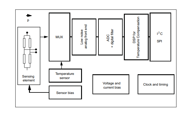
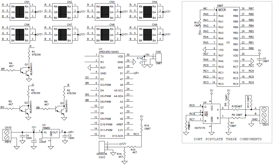
We have seen a series of Linux-based SBCs the last few months, like the next-gen BeagleBone AI, maker boards from Google and Nvidia, to mention just a few. The SBC market is booming right now, infact a recent Global Market Insights report projects that the SBC market will grow from $600 million in 2018 to $1 billion by 2025. The new trend of IoT and AI-enabled edge computing, gives rise to new boards being rolled off. Let’s see the top 10 boards to look forward for 2019.

1. UP Xtreme

This is the latest of Aaeon’s line of community-backed SBCs which taps Intel’s 8th Gen Whiskey Lake-U CPUs, and maintains 15W TDP with performance boosted up to quad-core, dual threaded configurations.

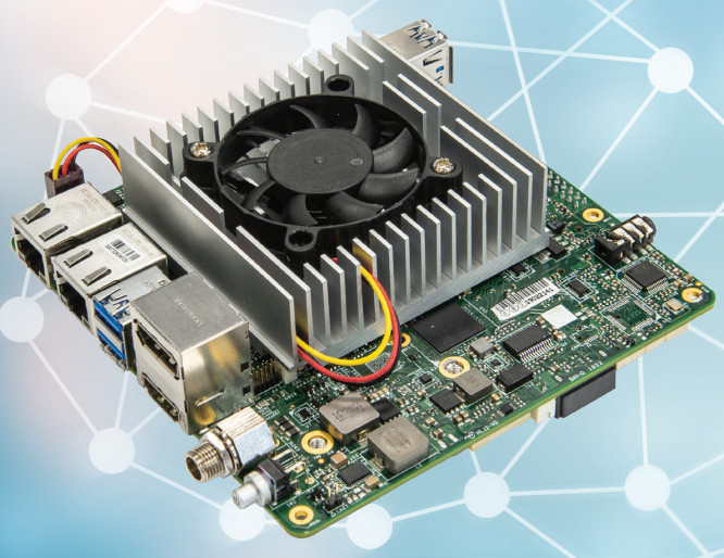
The SBC enables up to 16GB DDR4, 128GB eMMC and offers 4K displays via HDMI, DisplayPort, and eDP. It also features SATA, 2x GbE, 4x USB 3.0, and 40-pin “HAT” and 100-pin GPIO add-on board connectors. Mini-PCIe and dual M.2 slots are available. The dual M 2 slots supports wireless modems and more SATA options, they also support Aaeon’s new AI Core X modules, that offers Intel’s latest Movidius Myriad X VPUs for 1TOPS neural processing acceleration.

2. Jetson Nano Dev Kit

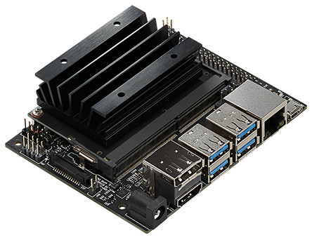
Nvidia has announced a low-end Jetson Nano compute module which is a smaller (70 x 45mm) version of the old Jetson TX1. It enables 4x Cortex-A57 cores and has a lower-end 128-core Maxwell GPU. The module offers 2GB and 8GB of RAM and flash. It supports 4K video and the GPU offers similar CUDA-X deep learning. It costs $99, supported by a forum and other community resources. It has 40-pin GPIO, an M.2 slot, GbE with Power-over-Ethernet, HDMI 2.0 and eDP links, and 4x USB 3.0 ports.

3. Coral Dev Board

Earlier this month, Google announced its first Linux maker board which features an NXP i.MX8M and Google’s Edge TPU AI chip. The Raspberry Pi-like Coral Dev Board was accompanied by an Edge TPU-enabled Coral USB Accelerator USB stick, then will be followed by an Edge TPU based Coral PCIe Accelerator and a Coral SOM compute module. The devices come with schematics, community resources, and other open-spec resources. The Board features the Edge TPU chip with NXP’s quad-core, 1.5GHz Cortex-A53 i.MX8M, a 3D Vivante GPU/VPU and a Cortex-M4 MCU. The Board offers 4K-ready GbE, HDMI 2.0a, 4-lane MIPI-DSI and CSI, and USB 3.0 host and Type-C ports.

4. SBC-C43

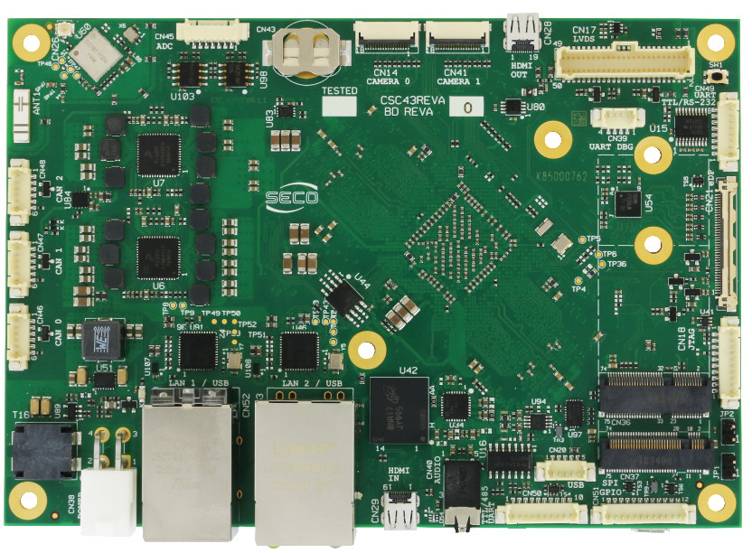
Seco’s SBC-C43 board is the pioneer SBC based on NXP’s high-end, up to hexa-core i.MX8. The SBC supports the i.MX8 QuadMax with 2x Cortex-A72 cores and 4x Cortex-A53 cores, the QuadPlus has a single Cortex-A72 and 4x -A53, and the Quad has no -A72 cores and 4x -A53. The SBC-C43 enables up to 8GB DDR4 and 32GB eMMC. It features dual GbE, HDMI 2.0a in and out ports, WiFi/Bluetooth, and a series of industrial interfaces. Its dual M.2 slots enable SATA, wireless, and more.

5. Nitrogen8M_Mini

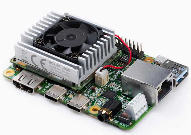
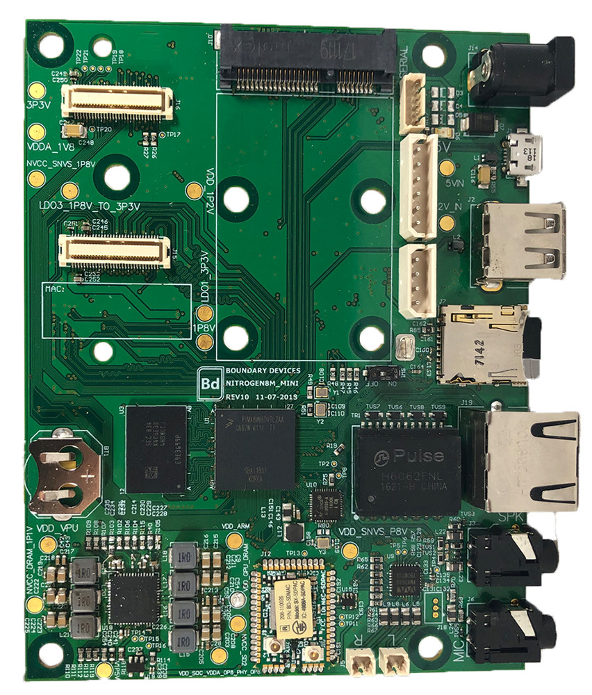
The open-spec Nitrogen8M_Mini from Boundary Device is the first SBC to feature NXP’s new i.MX8M Mini SoC. The Mini utilizes a more advanced 14LPC FinFET process than the i.MX8M, which results in lower power consumption and higher clock rates for both the 4x Cortex-A53 (1.5GHz to 2GHz) and Cortex-M4 (400MHz) cores. With Linux and Android support, the Nitrogen8M_Mini ships with 2GB to 4GB LPDDR4 RAM and 8GB to 128GB eMMC. Its MIPI-DSI and -CSI interfaces support optional touchscreens and cameras, respectively. It offers a GbE port, and PoE and WiFi/BT are optional. It also features 3x USB ports, one or two PCIe slots, and optional -40 to 85°C support. It is available for $135, and shipping due this spring.

6. Pine H64 Model B

Pine64’s latest hacker board, is part of an open source product, which also includes a laptop, tablet, and phone. Recently going on sale for $39 (2GB) or $49 (3GB), the Raspberry Pi semi-clone composes of the high-end, but low-cost Allwinner H64. The quad -A53 SoC offers 4K video with HDR support.

The Model B enables up to 128GB eMMC storage, WiFi/BT, and a GbE port. I/O features includes 2x USB 2.0 and single USB 3.0 and HDMI 2.0a ports plus SPDIF audio and an RPi-like 40-pin connector.

7. AI-ML Board

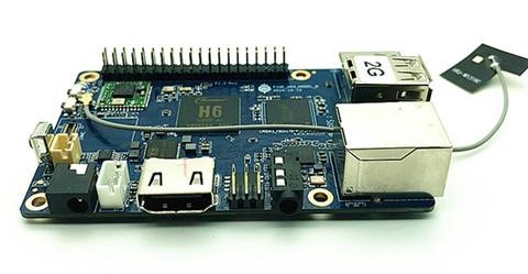
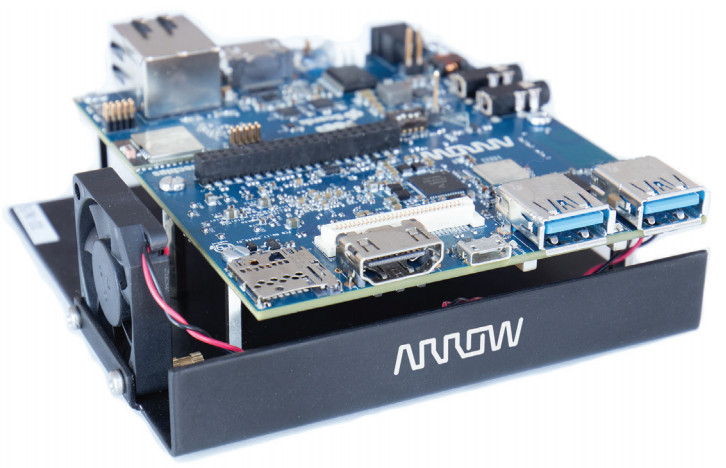
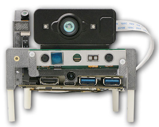
Arrow announced the i.MX8X based SBC earlier this month along side a similarly 96Boards CE Extended format, i.MX8M based Thor96 SBC. The AI-ML Board seems to be the first SBC that features the low-power i.MX8X, which enables up to 4x 64-bit, 1.2GHz Cortex-A35 cores, a 4-shader, 4K-ready Vivante GPU/VPU, a Cortex-M4F chip, and a Tensilica HiFi 4 DSP.

The board offers 2GB LPDDR4, Ethernet, WiFi/BT, and a pair each of MIPI-DSI and USB 3.0 ports. It is expected to launch by June 1.

8. BeagleBone AI

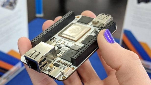
The AI is enabled by dual TI C66x DSPs and four embedded-vision-engine (EVE) neural processing cores. BeagleBoard.org claims that calculations for computer-vision models using EVE run at 8x times the performance per watt compared to the similar, but EVE-less, AM5728. The EVE and DSP chips are supported through a TIDL machine learning OpenCL API and pre-installed tools. The AI is based closely on the BeagleBone Black and offers backward header, mechanical, and software compatibility. It offers 1GB RAM and 16GB eMMC storage. It is due to go on sale for $100 in April.

9. Robotics RB3 Platform (DragonBoard 845c)

The 10nm, octa-core, “Kryo” based Snapdragon 845 is one of the most powerful Arm SoCs available. It features an advanced Adreno 630 GPU with “eXtended Reality” (XR) VR technology and a Hexagon 685 DSP with a third-gen Neural Processing Engine (NPE) for AI applications. The $449 and up kit features the board’s expansion connectors, which are pre-stocked with Qualcomm cellular and robotics camera mezzanines. The kit also includes standard 4K video and tracking cameras, with optional Time-of-Flight (ToF) and stereo SLM camera depth cameras. The SBC runs Linux with ROS (Robot Operating System).

10. Avenger96

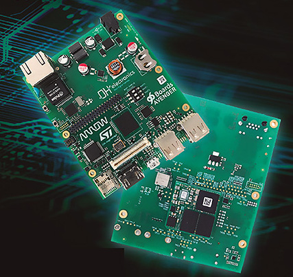
The Avenger96 is a 96Boards CE Extended SBC designed for low-power IoT applications. However, the SBC features a more power-efficient, but slower SoC (ST’s recently announced STM32MP153). The Avenger96 has dual, 650MHz Cortex-A7 cores, a Cortex-M4, and a Vivante 3D GPU.

The board features an Avenger96 module with the STM32MP157 SoC and offers 1GB of DDR3L, 2MB SPI flash, and a power management IC. The Avenger96 SBC is equipped with GbE, HDMI, micro-USB OTG, and dual USB 2.0 host ports. Available also is a microSD slot, and 40- and 60-pin GPIO connectors. The board is expected to go on sale in April.

For further information visit Linux.com

LMR36015 – 4.2-V to 60-V, 1.5-A ultra-small synchronous step-down converter

The LMR36015 regulator is an easy-to-use, synchronous, step-down DC/DC converter. With integrated high-side and low-side power MOSFETs, up to 1.5 A of output current is delivered over a wide input voltage range of 4.2 V to 60 V. Tolerance goes up to 66 V. The transient tolerance reduces the necessary design effort to protect against overvoltages and meets the surge immunity requirements of IEC 61000-4-5.

The LMR36015 uses peak-current-mode control to provide optimal efficiency and output voltage accuracy. Load transient performance is improved with FPWM feature in the 1-MHz regulator. Precision enable gives flexibility by enabling a direct connection to the wide input voltage or precise control over device start-up and shutdown. The power-good flag, with built-in filtering and delay, offers a true indication of system status eliminating the requirement for an external supervisor.

The LMR36015 is in a HotRod™ package which enables low noise, higher efficiency, and the smallest package to die ratio. The device requires few external components and has a pinout designed for simple PCB layout. The small solution size and feature set of the LMR36015 are designed to simplify implementation for a wide range of end equipment, including space critical applications of ultra-small field transmitters and vision sensors.

Features


  • Designed for reliable and rugged applications
    • Input transient protection up to 66 V
    • Junction temperature range –40°C to +150°C
    • Protection features: thermal shutdown, input undervoltage lockout, cycle-by-cycle current limit, hiccup short-circuit protection
    • HotRod™ package enables low noise and minimized switch node ringing
    • 0.4-V dropout with 1.5-A load (typical)
  • Suited for scalable industrial power supplies
    • Pin compatible With:
    • 400-kHz, 1-MHz Frequency options
    • Low power dissipation across load spectrum
      • 90% efficiency at 400 kHz (24VIN, 5VOUT, 1A)
      • 93% efficiency at 400 kHz (12VIN, 5VOUT, 1A)
      • Increased light load efficiency in PFM
      • Low operating quiescent current of 26 µA
    • Small 2-mm × 3-mm HotRod™ package
    • solution with few external components

more information: http://www.ti.com/product/LMR36015

HS101: A high quality, and Cheap DIY Oscilloscope

HS101 Demo

The Oscilloscope is a test instrument used for the visualization and observation of varying signal voltages, usually as a two-dimensional plot with one or more signals plotted against time. They are used in the design and debugging of electronic devices to view and compare waveforms, determine voltage levels, frequency, noise and other parameters of signals applied at its input as it changes with time. This makes Oscilloscopes a very important tool on the desk of an electronics engineer or maker. However, Oscilloscopes are quite expensive, they cost between $45 – $100 for a small oscilloscope and above $300 for advanced oscilloscopes, which puts them beyond the reach of basic users. But what if we could create something cheaper, compact, and highly functional using the components familiar to makers? That is the question that led to today’s tutorial.

For today’s tutorial, we will build the HS101 Oscilloscope. The HS101 Oscilloscope setup comprises of the HS101 portable and compact DIY oscilloscope, connected to an Android-based mobile phone or tablet running the HScope app.  The oscilloscope is based on the STM32F103 microcontroller which has 2 fast, 12-bits ADC and it samples the signal to be examined (after it has passed  condition elements, like a network of resistors capacitors and diodes) on board.

HS101: A high quality, and Cheap DIY Oscilloscope – [Link]

HS101: A high quality, and Cheap DIY Oscilloscope

One of the most interesting thing about being a maker is you never get tool-stranded, with the right components, makers tend to have the ability to build makeshift tools on the go. Today, we will take a look on how to build a cheap version of one of the most important tools for any electronics engineer or maker; The Oscilloscope.

An Oscilloscope – source: sparkfun.com

The Oscilloscope is a test instrument used for the visualization and observation of varying signal voltages, usually as a two-dimensional plot with one or more signals plotted against time. They are used in the design and debugging of electronic devices to view and compare waveforms, determine voltage levels, frequency, noise and other parameters of signals applied at its input as it changes with time. This makes Oscilloscopes a very important tool on the desk of an electronics engineer or maker. However, Oscilloscopes are quite expensive, they cost between $45 – $100 for a small oscilloscope and above $300 for advanced oscilloscopes, which puts them beyond the reach of basic users. But what if we could create something cheaper, compact, and highly functional using the components familiar to makers? That is the question that led to today’s tutorial.

HS101 in Action

For today’s tutorial, we will build the HS101 Oscilloscope. The HS101 Oscilloscope setup comprises of the HS101 portable and compact DIY oscilloscope, connected to an Android-based mobile phone or tablet running the HScope app.  The oscilloscope is based on the STM32F103 microcontroller which has 2 fast, 12-bits ADC and it samples the signal to be examined (after it has passed  condition elements, like a network of resistors capacitors and diodes) on board.

Some of the features of the HS101 includes;

  • Single Channel Oscilloscope
  • 12 Bits ADC resolution
  • 0-20v Input voltage range
  • Sampling rates between 3KS/s – 1800KS/s
  • Bandwidth 200kHz
  • Up to 100KSa/s continuous acquisition
  • Input noise depends on the sampling rate. < 15mV for sampling rate <=100KSa/s

The oscilloscope can be used in standard situations for tasks like DC measurements while also being useful for long period voltage logging and basic automobile checkups like;

  • Battery level logging
  • Battery Ignition Off Draw (IOD) data logging (with C650-like amp clamp or a DIY tool)
  • Alternator AC ripple level (example here)
  • In-Cylinder Compression Test (with 100 PSIG pressure sensor, example here

Required Components

The following components are required to build this project;

  1. STM32F103C8 Blue Pill
  2. USB to TTL Cable
  3. 1N4007 (2)
  4. 10K Resistor
  5. 2k Resistor
  6. 470pF Capacitor
  7. USB OTG Cable (Micro USB to Micro USB / USB Type-C to Micro USB)
  8. Perforated PCB Boards (anything with 6 to 7 holes should do it).
  9. 6 Pin single row female 2.54mm pin header (2)
  10. Probe and BNC Connector (plain wires or a 3.5mm audio jack can be also be used)

You could also decide to make a Printed circuit board for this project. The BOM, Schematics and the PCB design are attached under the download section of this tutorial.

Schematics

The schematics for this project is unbelievably easy. The Input module comprising of the resistors, capacitors, and diodes is built/soldered on the perforated (proto) board and then mounted on the STM Blue Phil board using the female headers which plug directly into the Blue Phil. This makes the design modular and compact. Connect the components on the protoboard as shown in the schematics below.

Input Module Schematics

After soldering the parts, plug the input module on the STM Blue pill as shown in the image below.

Plug Input Module on Blue Pill

As mentioned above, you could make your own fully customized PCB-based Oscilloscope using the same design for this project. All the files you need including BOM and the PCB are attached under the download section at the end of the tutorial. An image of the PCB version is shown below.

HS101 PCB

Flashing the Firmware

One of the cool things about today’s project is the fact that we will be uploading code to the microcontroller board using a smartphone, which means you don’t need your computer for any part of this project. For today’s tutorial, we will use the STM32 Utils App by Martin Loren. The app comes preloaded with the firmware for the HS101 oscilloscope, so all we need do is to connect the Blue pill microcontroller to your phone via a USB to Serial converter and an OTG cable as shown in the image below.

Flash Firmware Using STM32Utils. (Credit:Time4ee)

The pin map for the connection of the serial to USB cable and the STM32 Blue pill is shown below;

Blue Pill – USB-UART

5V - 5V(or VBus)
PA9 - Rx
PA10 - TX
GND - GND

with the connections done,  press the “Init Chipset” button on the app. You should see the light on the STM come up. Click the “DIY Library” button on the app, select the HS101 Firmware, and click on “Flash Firmware“.

With the firmware upload complete, you can then disconnect the USB to Serial cable and connect the board to the phone via the OTG cable.

That’s it, your oscilloscope is ready!

Demo

The STM32 is powered by the smartphone via the OTG cable. As soon as it is connected to the phone, the red led of the Blue Pill board should come on. As soon as the STM32 is on, open the HScope app. The app should automatically recognize the oscilloscope and start displaying data.

Connect any signal to the input of the HS101 and you should see the data displayed on the app as shown below.

HS101 Demo

The free-version of HScope app allows using the HS101 as voltage tester and as a simple oscilloscope which might be enough for simple tasks. The full version of the HScope app, on the other hand, provides access to real-time statistics, FFT and could be used to convert the HS101 to a data logger.

Optimizing the Oscilloscope

Noise is the biggest challenge of the HS101 oscilloscope. It is strongly dependent on the phone model and this can be fairly overcome by adding capacitors between GND and 3.3V pins on the Blue Pill board. The value of the capacitor closest to the USB connector can be around 470uF for improvement in data quality.

The Oscilloscope described by this tutorial might not necessarily be capable of replacing the standard Lab Oscilloscope, but this would help you get some of the little tasks done fast, without having to pay huge sums. It is also portable which makes it useful if you move around a lot.

That’s it for today’s tutorial guys. Feel to reach out to me via the comment section if you have any questions or difficulty while replicating the tutorial.

Sources:

Azure Sphere MT3620 Starter Kit for Creating Secured IoT Edge Devices

Avnet Kit
Azure Sphere MT3620 Starter Kit

Last year, Microsoft signed with Avnet as a strategic partner for their Azure platform – a platform for robust cloud computing. This partnership is expected to help boost the already fragile IoT market and adds some level of reputation to it considering Avnet is a big name in the electronics industry and Microsoft a top brand in the software world.

Security is an utmost priority in the growing Internet of Things market. So, to make it end to end secure, a lot of effort have been put to introduce different setups like handshaking, encryption and many more. A breach in security in IoT might not only affect the product in the short run but also impact on the personal brand of the organization.

Highly secured end to end IoT implementations cannot be overemphasized on and with the flood of several IoT development kits, developers might be easy fall prey to unsecured solution setups. Avnet has unveiled the Azure Sphere MT3620 Starter Kit, which supports rapid prototyping of IoT implementations using Microsoft’s Azure Sphere — an end-to-end solution for creating highly-secured, connected microcontroller devices.

Azure Sphere MT3620 Starter Kit

The starter kit launched is built around the Avnet Azure Sphere module which is based on the MT3620 reference development board. The MT3620 is a highly integrated, high-performance IoT MCU with the high level of security necessary for modern, robust internet-connected devices. The MT3620 targets a wide range of IoT applications including smart home, commercial, industrial and many other domains thanks to its extensive I/O peripheral subsystem that allows device design flexibility and freedom.

The starter kit can easily find application in the below markets:

  • Consumer appliances
  • Smart retail.
  • Remote access
  • Building automation software.
  • Factory automation applications.

Specifications:

  • Two MikroEClick Board expansion sockets
  • Built-in Microsoft security.
  • Connectivity: Wi-Fi.
  • Processor: Arm Cortex-A7
  • Grove expansion connector (I2C)
  • Onboard sensors
  • 3-Axis accelerometer
  • 3-Axis Gyro
  • Temperature
  • Pressure/Barometric
  • Interface for optional OLED 128×64 display
  • USB Interface
  • Supports debug, service and recovery UARTs, and JTAG
  • User push switches and LEDs
  • 5V to 3.3V Power regulation
  • DC Supply Input:
  • USB 5V from the host computer
  • Terminal footprints for external 5VDC and VBAT supplies
  • Azure Sphere MT3620 Module features include:
  • MediaTek MT3620AN SoC
  • 3x ISU interfaces pre-configured for UART, SPI, I2C
  • ADC/GPIO: 3x 12-bit ADC inputs (or 3 GPIOs)
  • PWM/GPIO: 9x PWM outputs (or up to 24 GPIOs)
  • RTC (requires VBAT supply)
  • Dual-band 2.4/5GHz 802.11 a/b/g/n WiFi
  • Dual-band 2.4/5GHz chip antenna
  • Production-ready

Azure Sphere MT3620 module is a 33 x 22 mm module and packs a dual-band Wi-Fi chip antenna and a system clock. It provides support of up to 27 configurable GPIOs, including support for UART, I2C, and SPI.

The MT3620 starter kit includes a carrier board that connects the Azure Sphere MT3620 module I/Os to a pair of MikroE sockets, I2C grove connector, OLED graphical display connector, 3D accelerometer & gyro, temperature and light sensors. All of this together, when put in order, the connected device in harmony with each other will give the best of their results. A 5 V power is applied to the board, due to the in-built debugging. Debugging is achieved through USB to UART interface.

The Avnet Azure Sphere MT3620 Starter Kit is now available for purchase for $75 from Avnet. More information can be found on the product and announcement page.

LPS33W – MEMS pressure sensor withstands harsh environment

MEMS pressure sensor: 260-1260 hPa absolute digital output barometer with potted gel package.

STMicroelectronics LPS33W MEMS Pressure Sensor is ultra compact and functions as a digital output barometer. The LPS33W combines a sensing element and an IC interface which communicates through I2C or SPI from the sensing element to the application. Detecting absolute pressure, the sensing element consists of a suspended membrane manufactured using a dedicated process developed by ST.

The LPS33W is available in a ceramic LGA package with metal lid, and is guaranteed to operate over a temperature range extending from -40°C to +85°C. The package is holed to allow external pressure to reach the sensing element, and gel inside the IC protects the electrical components from harsh environmental conditions.

LPS33W Pressure Sensor

Key Features

  • Pressure sensor with potted gel package
  • 260 to 1260hPa absolute pressure range
  • Current consumption down to 3μA
  • High overpressure capability: 20x full scale
  • Embedded temperature compensation
  • 24-bit pressure data output
  • 16-bit temperature data output
  • ODR from 1Hz to 75Hz
  • SPI and I²C interfaces
  • Embedded FIFO
  • Interrupt functions: data-ready, FIFO flags, pressure thresholds
  • Supply voltage: 1.7 to 3.6V
  • ECOPACK® lead-free compliant

The LPS33W operates at just 15µA in high-performance mode, with a 3µA low-power mode and 1µA power-down to help maximize runtime of battery-powered devices. A generous 128-bit FIFO stores up to 40 slots of 32-bit pressure and temperature data, helping save extra power by minimizing intervention from the host microcontroller. A low-pass filter and I2C and SPI digital interfaces are also built-in.

LPS33W Block Diagram

The LPS33W is in mass production now, in a 3.3mm-diameter x 2.9mm cylindrical metal case, priced from $3.60 for orders of 1000 pieces. For more information, visit www.st.com/lps33w-pr

15% Off – Exclusive Farnell Offer

Get 15% discount off Farnell products until the 30th April when buying via OEMsecrets.com

You’ll just need to select the correct code based on your location and apply at checkout with Farnell, when clicking to “Buy Now” through our site. Click the View Offer button below for more information and to claim your discount code.

[VIEW OFFER]

See the most popular codes below. Click Here for a full list of codes and terms.

  • OEMSEU for EU
  • OEMS15UK for United Kingdom
  • OEMS15US for United States
  • OEMS15IN for India

8 RGB LED Driver Shield for Arduino Nano with Optical Defuse Sensor

The board consists of 8 x RGB LEDs 1W, BJT transistors on each LED, series resistor across the LED for current limiting, a hole to mount 18mm optical sensor which may be a defuse sensor for object detection with Arduino nano.  The board can be programed to create multiple RGB LED related applications, like interactive lamp, automatic bathroom light etc. I have used Omron E3F-D32 defuse optical sensor which can detect human or object at a distance up to 300mm. When the sensor detect any object within the range of 300mm its toggles output. The output is PNP type, the range of sensor is adjustable using trimmer pot and also sensor has LED operation indicator. All RGB LED transistors connected to D3, D5, D6 of Arduino PWM pins which helps to create multi-color effects. Optical sensor connected to digital pin D13 of Arduino Nano. Board also has prototype area to mount other sensors or circuitry and some additional components are provided to make PIC based applications or RS485 based RGB LED controller. Circuit works with 12V DC input.

8 RGB LED Driver Shield for Arduino Nano with Optical Defuse Sensor – [Link]

8 RGB LED Driver Shield for Arduino Nano with Optical Defuse Sensor


The board consists of 8 x RGB LEDs 1W, BJT transistors on each LED, series resistor across the LED for current limiting, a hole to mount 18mm optical sensor which may be a defuse sensor for object detection with Arduino nano.  The board can be programed to create multiple RGB LED related applications, like interactive lamp, automatic bathroom light etc. I have used Omron E3F-D32 defuse optical sensor which can detect human or object at a distance up to 300mm. When the sensor detect any object within the range of 300mm its toggles output. The output is PNP type, the range of sensor is adjustable using trimmer pot and also sensor has LED operation indicator. All RGB LED transistors connected to D3, D5, D6 of Arduino PWM pins which helps to create multi-color effects. Optical sensor connected to digital pin D13 of Arduino Nano. Board also has prototype area to mount other sensors or circuitry and some additional components are provided to make PIC based applications or RS485 based RGB LED controller. Circuit works with 12V DC input.

Features

  • Supply 12V DC
  • 8 RGB LEDs Each 1W
  • Defuse Reflective Sensor for Interactive Light
  • PCB Diameter 92.06 MM

Schematic

Parts List

Connections

Photos

OMRON E3F3 Photoelectric Sensor Datasheet

Video

TOP PCB Companies